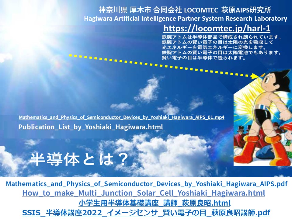
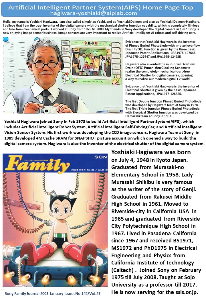
合同会社LOCOMTEC/萩原aips研究所
Hagiwara_AIPS_Laboratory.html
Publication_List_by_Yoshiaki_Hagiwara_AIPS.pdf
TOP_Page 001 ,
002 ,
003 ,
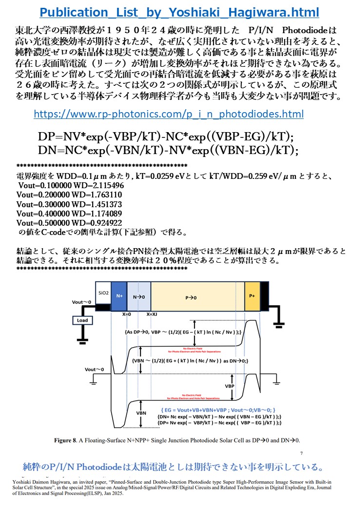
004 ,
005 ,
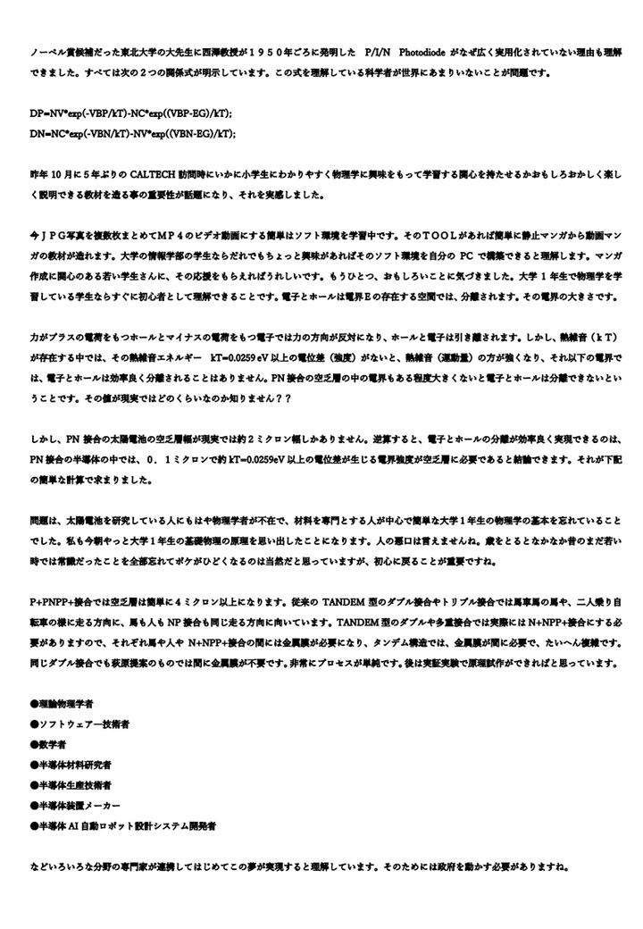
006 ,
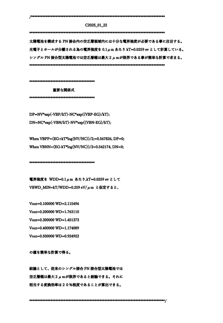
007 ,
008 ,
009 ,
010 011 ,
012 ,
013 ,
014 ,
015 ,
016 ,
017 ,
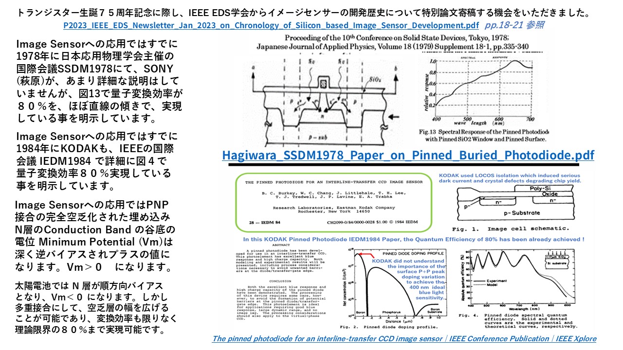
018 ,
019 ,
020 021 ,
022 ,
023 ,
024 ,
025 ,
026 ,
027 ,
028 ,
029 ,
030 031 ,
032 ,
033 ,
034 ,
035 ,
036 ,
037 ,
038 ,
039 ,
040 041 ,
042 ,
043 ,
044 ,
045
Page001_萩原トミエの絵手紙
萩原トミエの絵手紙_Backup_2024年8月迄
2022年5月の萩原トミエの絵手紙雑記帳
Tomie_Hagiwara_E_Tegami_Backups(2022年4月から2026年7月迄).html
https://www.ogino-js.atsugi.ed.jp/new学校日記
Hagiwara_AIPS_Laboratory.html
Publication_List_by_Yoshiaki_Hagiwara.html
2026_08_03_ICDIS2026_Key_Note_by_Yoshiaki_Daimon_Hagiwara_AIPS.pdf
2026_07_08_ICCCAS2026_Key_Note_Slides_Head.pdf
2026_07_07_ICCCAS2026__IDCS26-8837_Slides_Head.pdf
Memo2026_06_25_半導体_尖端覇権の興亡_大鹿靖明著の読んで_萩原良昭.pdf
2026_06_23_AAIS_Certificate_of_Appointment_of_Associate_Editor_in_Chief_Yosiaki_Daimon_Hagiwara.pdf
https://aaia-ai.org/fellows?page=137
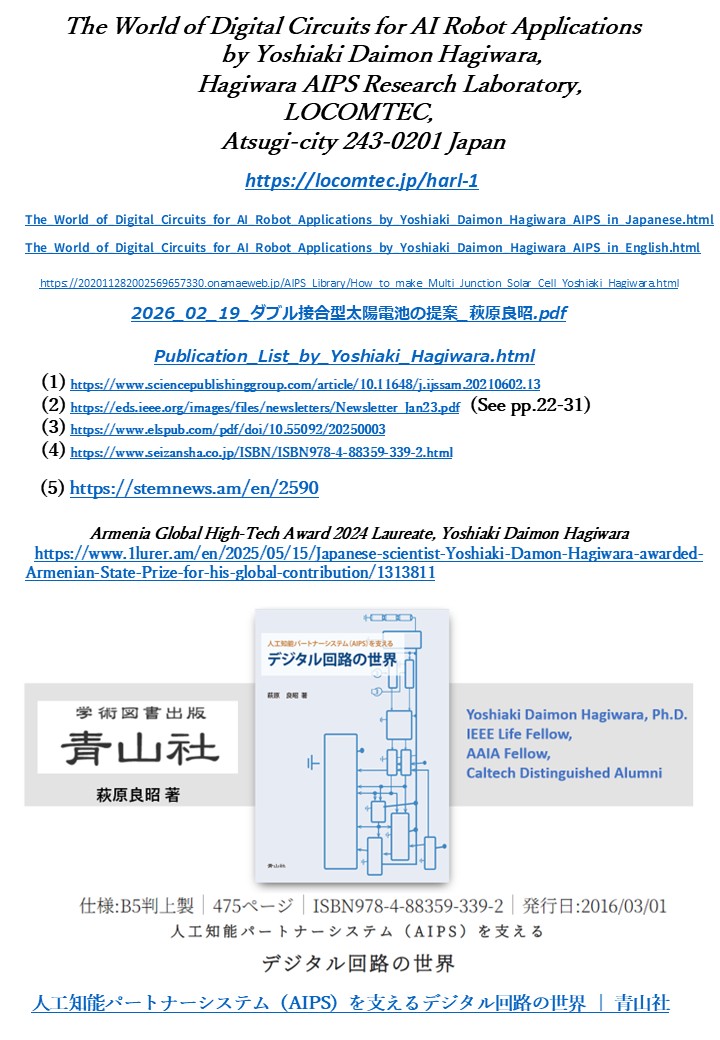
The_World_of_Digital_Circuits_for_AI_Robot_Applications_by_Yoshiaki_Daimon_Hagiwara_AIPS.pdf
The_World_of_Digital_Circuits_for_AI_Robot_Applications_by_Yoshiaki_Daimon_Hagiwara_AIPS_in_Japanese.html
The_World_of_Digital_Circuits_for_AI_Robot_Applications_by_Yoshiaki_Daimon_Hagiwara_AIPS_in_English.html
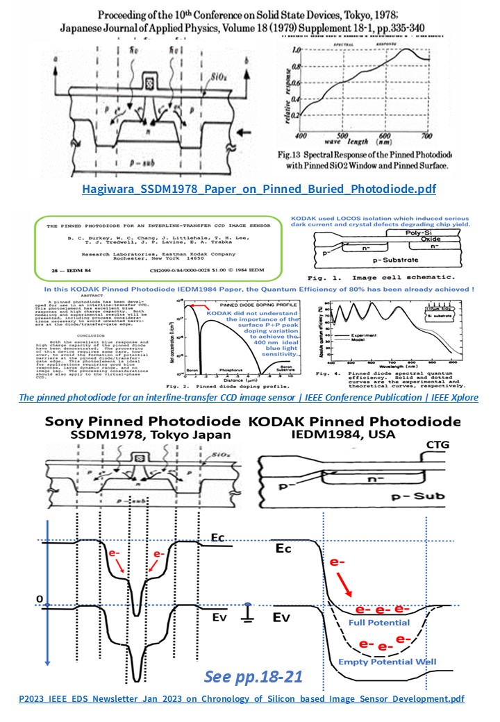
2026_05_27_Sony_SSDM1978_and_KODAK_IEDM1984_Papers_on_First_Pinned_Photodiode_Silicon_Chips.pdf
2026_05_26_Reverse-bias_PNP_Junction_Image_Sensor.pdf
https://globalitaward.am/en/laureates/yoshiaki-daimon-hagiwara
TOP_Page 001 ,
002 ,
003 ,
004 ,
005 ,
006 ,
007 ,
008 ,
009 ,
010 011 ,
012 ,
013 ,
014 ,
015 ,
016 ,
017 ,
018 ,
019 ,
020 021 ,
022 ,
023 ,
024 ,
025 ,
026 ,
027 ,
028 ,
029 ,
030 031 ,
032 ,
033 ,
034 ,
035 ,
036 ,
037 ,
038 ,
039 ,
040 041 ,
042 ,
043 ,
044 ,
045 萩原トミエの絵手紙_Backup_2024年8月迄
2022年5月の萩原トミエの絵手紙雑記帳
Tomie_Hagiwara_E_Tegami_Backups(2022年4月から2026年7月迄).html
https://www.ogino-js.atsugi.ed.jp/new学校日記
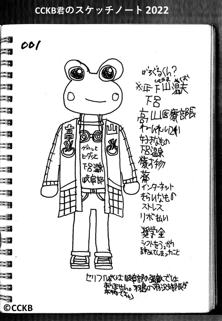
Page002 第05冊目_CCKB君のスケッチノート2022.html
第06冊目_CCKB君のスケッチノート2023_Sketch001~022.html
第07冊目_CCKB君のスケッチノート2023_Sketch023~049.html
第08冊目_CCKB君のスケッチノート_2023_03_16.html
第09冊目_CCKB君のスケッチノート_2023_04_02.html
第09A冊目_CCKB君のスケッチノート_2023_06_28.html
第10冊目_CCKB君のスケッチノート_2023_05_16.html
第11冊目_CCKB君のスケッチノート_2023_06_19.html
第12冊目_CCKB君のスケッチノート_2023_07_04.html
第13冊目_CCKB君のスケッチノート_2023_10_04.html
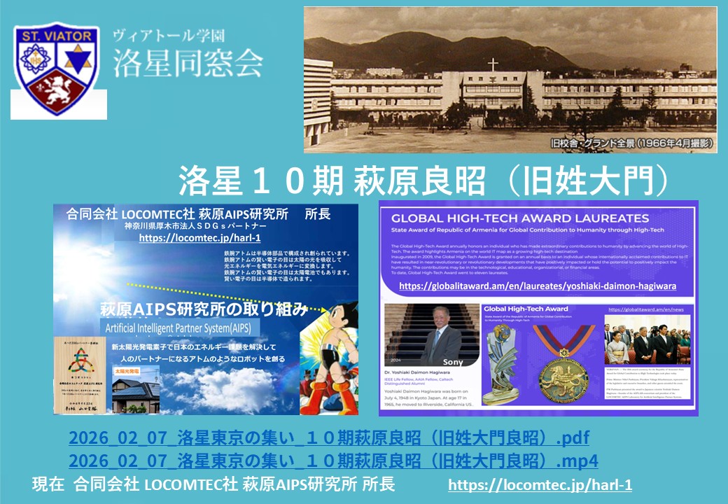
2026_02_07_洛星東京の集い_10期萩原良昭(旧姓大門良昭).pdf
京都洛星10期同窓会記念写真集
洛星東京の集い_2026
私の恩師でもあり敬愛する亡き義父の大門恒夫の映画作品
私の末っ子の可愛い実弟の大門実紀史の個人活動紹介
私のけんか相手ライバルだった敬愛する亡き実兄の萩原良巳の活動記録
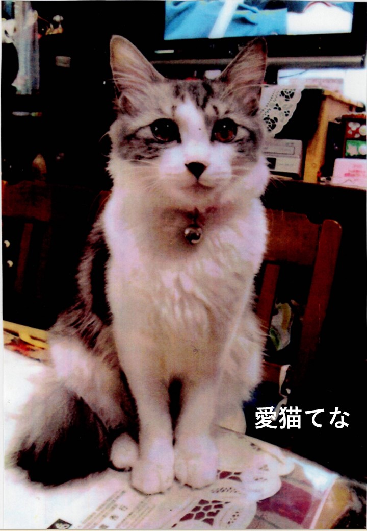
TENA.html
神奈川県全域「タウンニュース」_2019年1月18日掲載記事_萩原トミエ
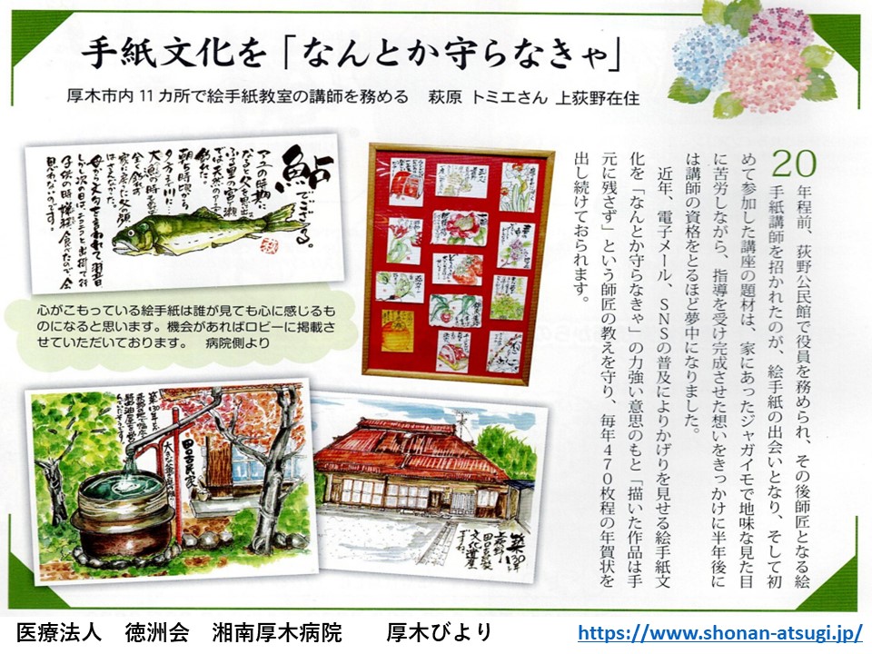
Page003 2019_Summer_厚木びより_Vol_26_Page_07_E_Tegami_by_Hagiwara_Tomie.pdf
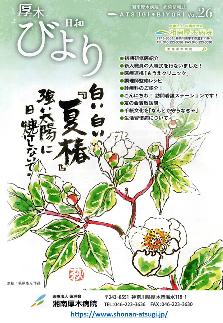
2019_Spring_厚木びより_Vol_26_表紙_E_Tegami_by_Hagiwara_Tomie.pdf
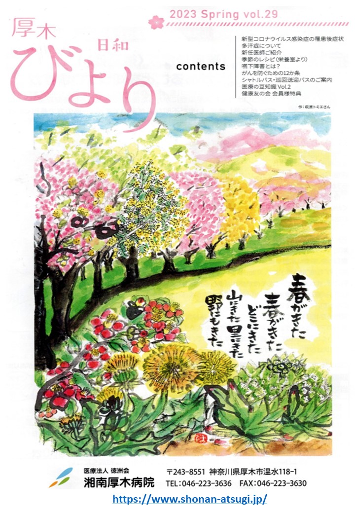
2023_Spring_厚木びより_Vol_29_表紙_E_Tegami_by_Hagiwara_Tomie.pdf
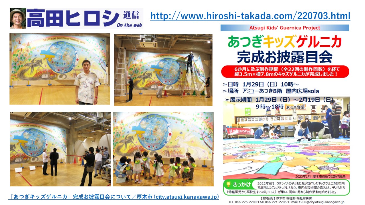
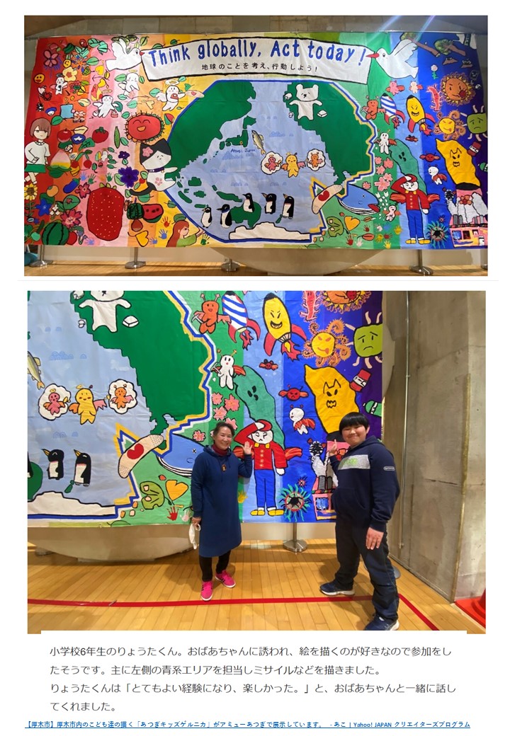
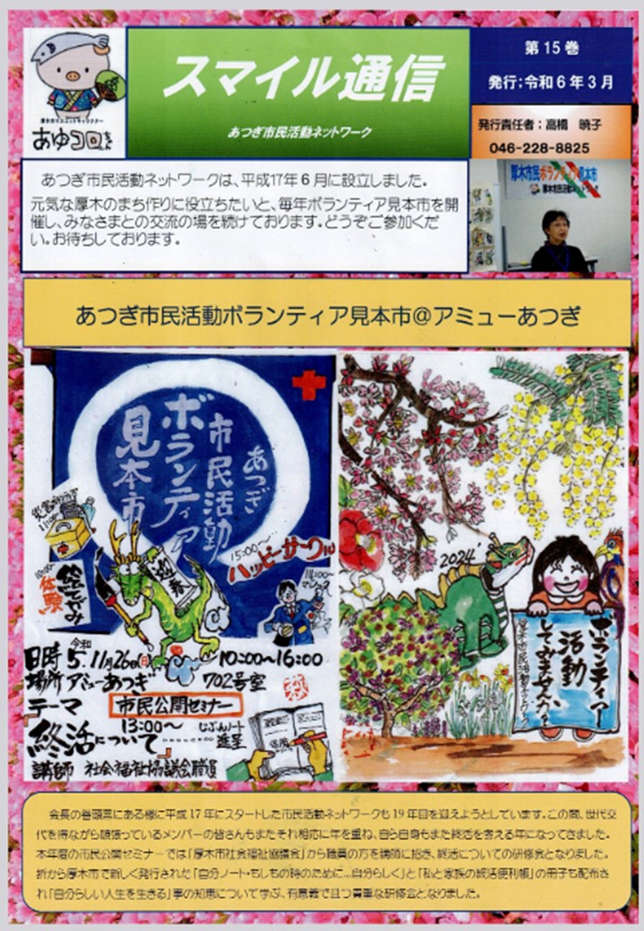
Atsugi-city_Kids_Gernica_Project_2023_1_29.pdf
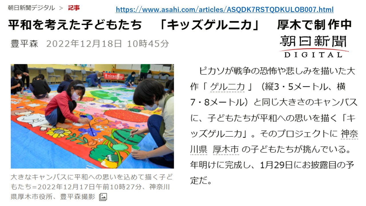
朝日新聞デジタル_2022_12_18_厚木市キッズゲルニカ.pdf
厚木キッズゲルニカ_2023_01_29.pdf
Atsugi-city_Kids_Gernica_Project_2023_1_29_creators.yahoo.co.jp(html)
https://www.asahi.com/articles/ASQDK7RSTQDKULOB007.html
朝日新聞デジタル_2022_12_18_厚木市キッズゲルニカ.pdf
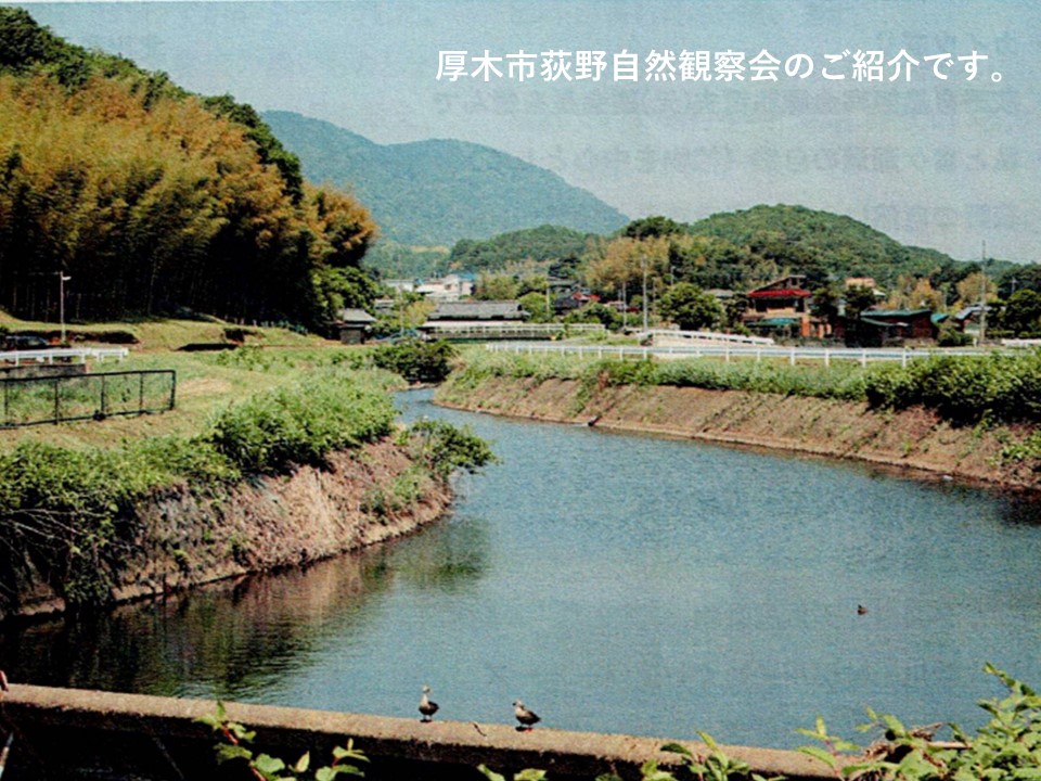
厚木市荻野自然観察会のご紹介.html
神奈川県厚木市のコミュニティカフェ荻野.html
鳶尾カフェの常連客の鈴木歩(あゆむ)さんの「厚木田独歩」パソコン写仏のご紹介です
鳶尾カフェの常連客の鈴木歩(あゆむ)さんの徒歩旅の記録です
Page004 カメラマン萩原昭紀の活動紹介.html
Hagiwara_Photo_Gallery.html
20220812_001.JPG
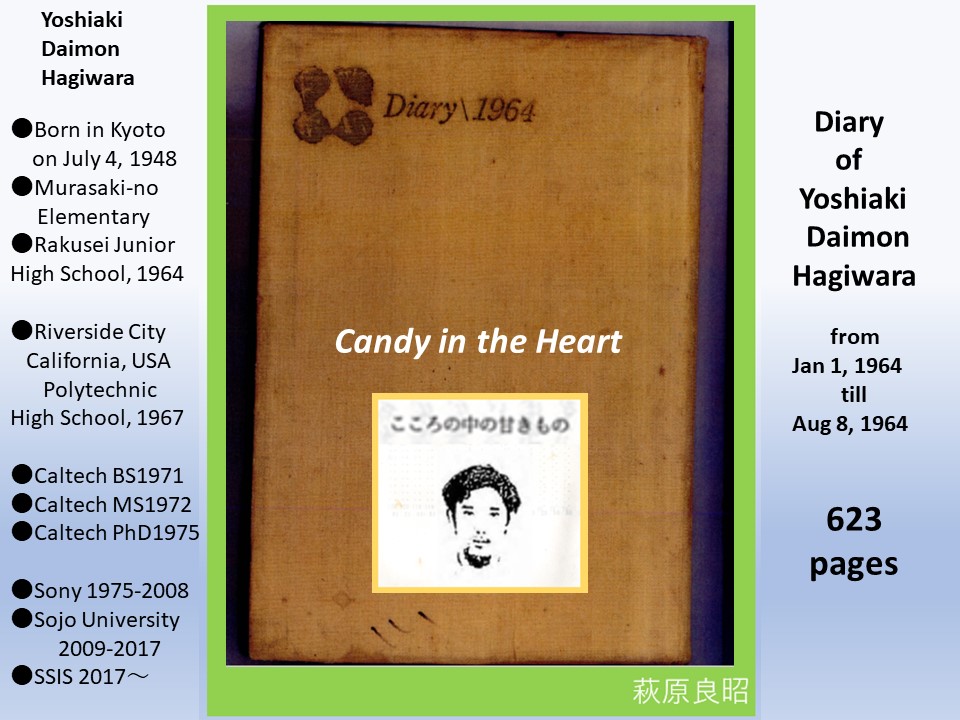
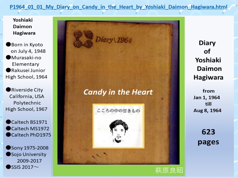
Page011 P1961_01_01_My_Diary_on_Candy_in_the_Heart/Candy_in_the_Heart.html
P1961_01_01_My_Diary_on_Candy_in_the_Heart/Candy_in_the_Heart.html
Page012 Enjoy_Korean_Language_for_Fun/index.html
TENA.html
京都洛星10期同窓会記念写真集
Hagiwara_履歴_2023_03_24.pdf
ソニー半導体OB会
ソニー半導体OB会記念写真2024年.pdf
Bio_and_List_of_Publications_Yoshiaki_Daimon_Hagiwara.pdf
Publication_List_by_Yoshiaki_Hagiwara.html
Jump to Page 5
Hagiwara_AIPS_Laboratory.html
TOP_Page 001 ,
002 ,
003 ,
004 ,
005 ,
006 ,
007 ,
008 ,
009 ,
010 011 ,
012 ,
013 ,
014 ,
015 ,
016 ,
017 ,
018 ,
019 ,
020 021 ,
022 ,
023 ,
024 ,
025 ,
026 ,
027 ,
028 ,
029 ,
030 031 ,
032 ,
033 ,
034 ,
035 ,
036 ,
037 ,
038 ,
039 ,
040 041 ,
042 ,
043 ,
044 ,
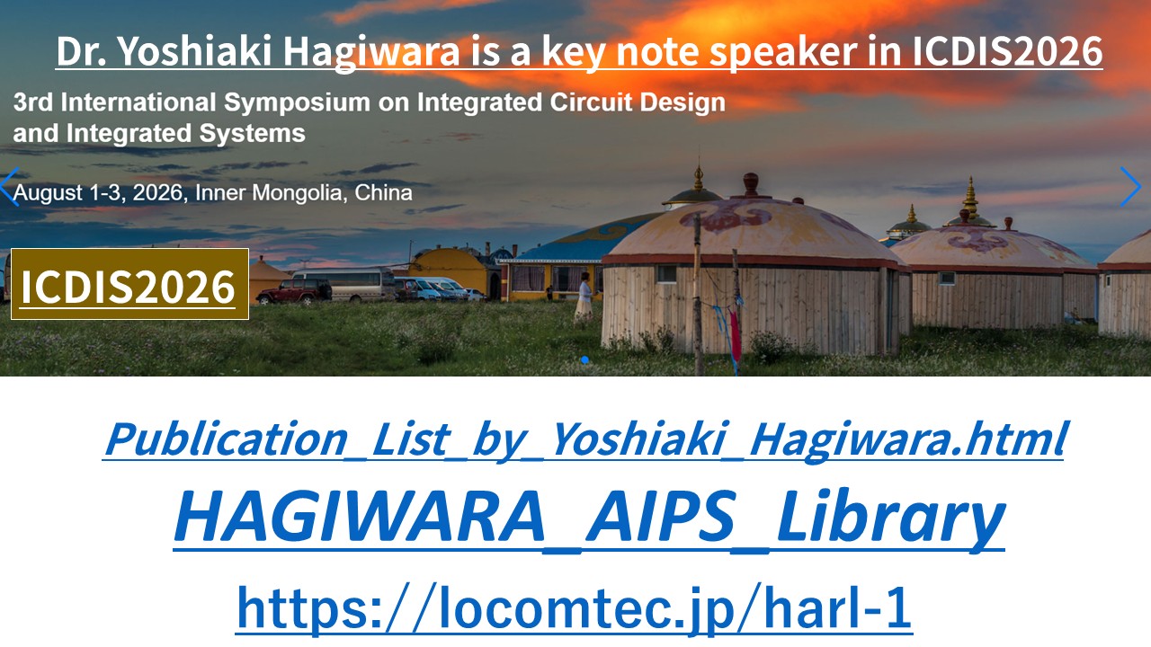
045 2026_08_01_ICDIS2026.pdf
ICDIS2026
Dr. Yoshiaki Hagiwara is a key note speaker in ICDIS2026
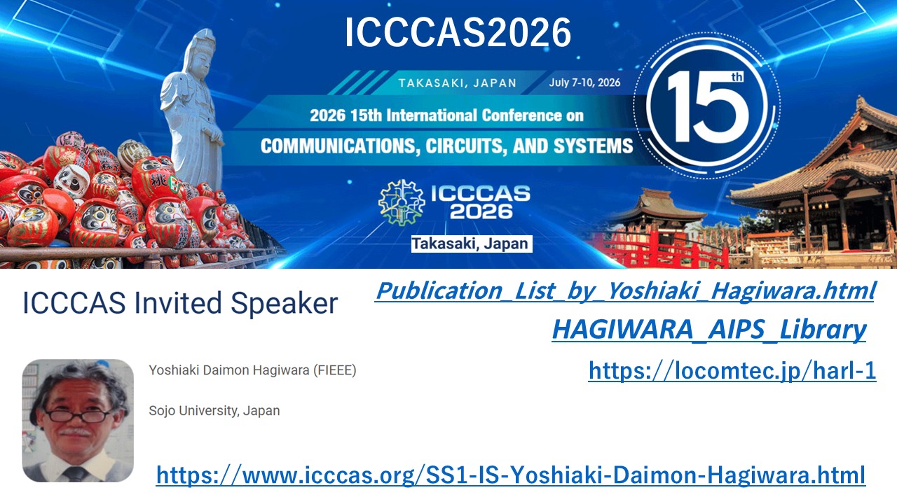
2026_07_01_ICCCAS2026.pdf
ICCCAS2026
Dr. Yoshiaki Hagiwara is an invited speaker in ICCCAS2026
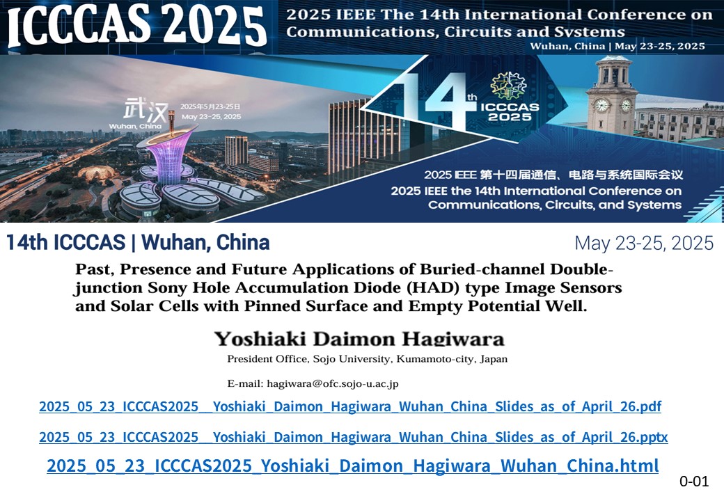
2025_05_23_ICCCAS2025_Yoshiaki_Daimon_Hagiwara_Wuhan_China_Slides.pdf
2025_05_23_ICCCAS2025_Yoshiaki_Daimon_Hagiwara_Wuhan_China_TEXT.pdf
2025_05_23_ICCCAS2025_Yoshiaki_Daimon_Hagiwara_Wuhan_China.mp4.
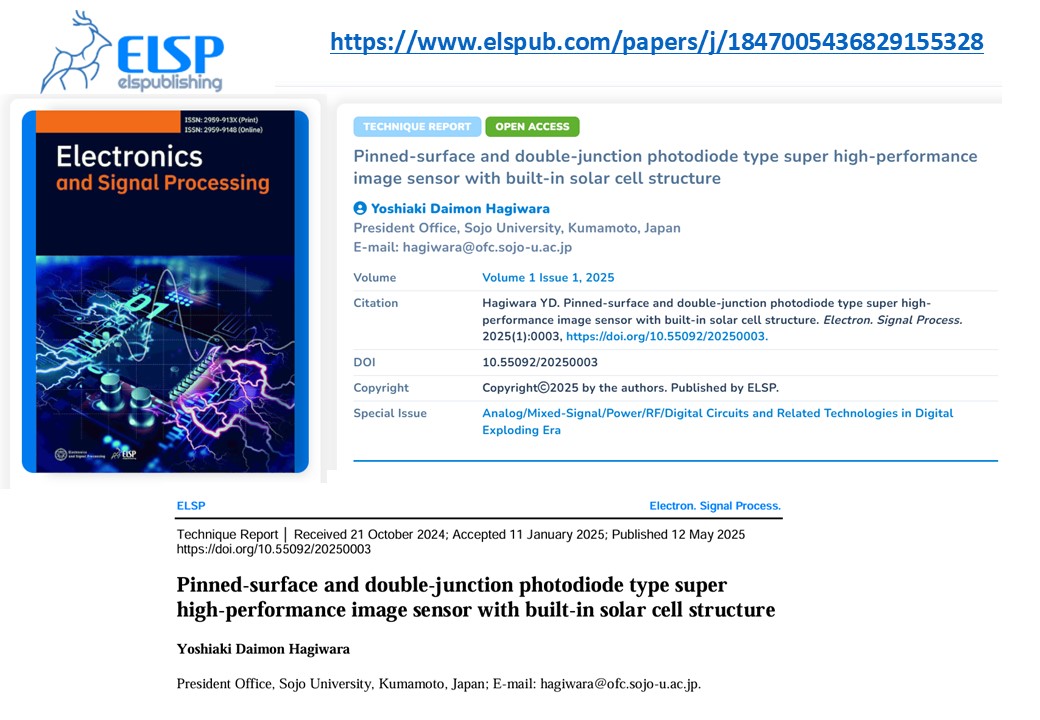
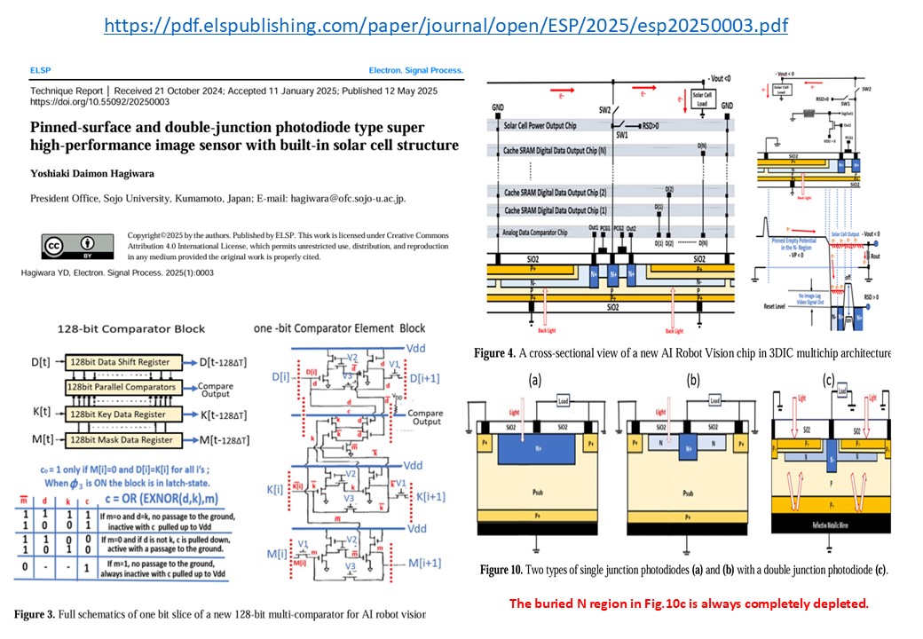
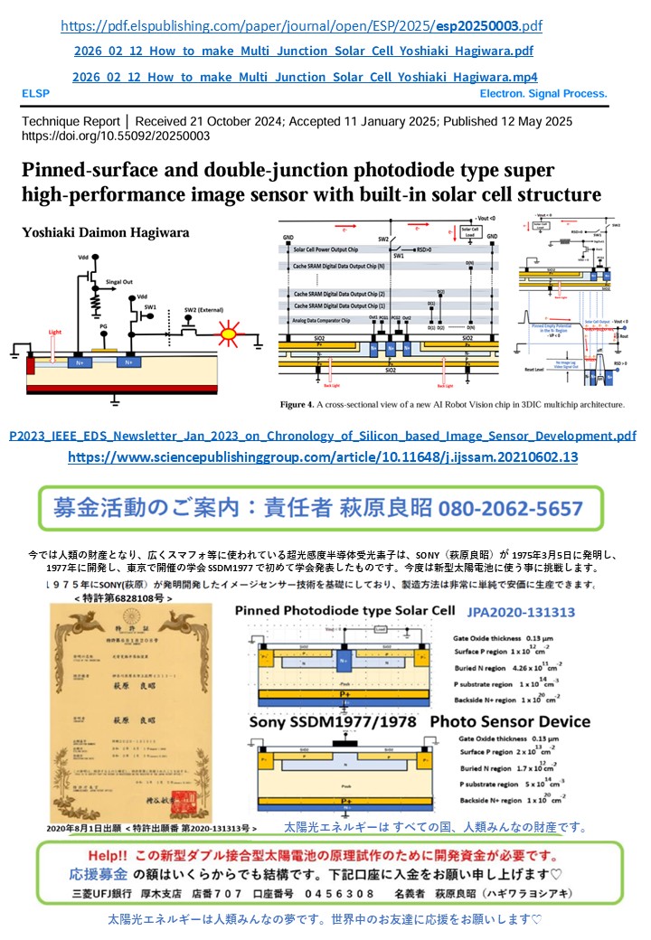
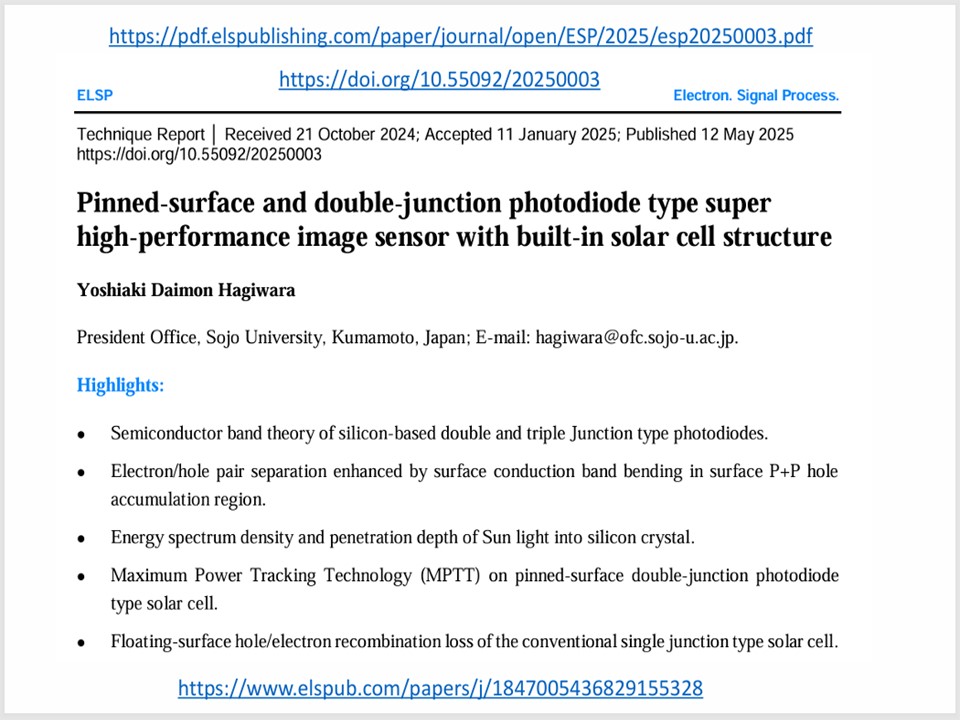
ESP2025_05_12_Image_Sensor_with_Built-in_Solar_Cell_Structure_by_Yoshiaki_Daimon_Hagiwara.pdf
https://pdf.elspublishing.com/paper/journal/open/ESP/2025/esp20250003.pdf
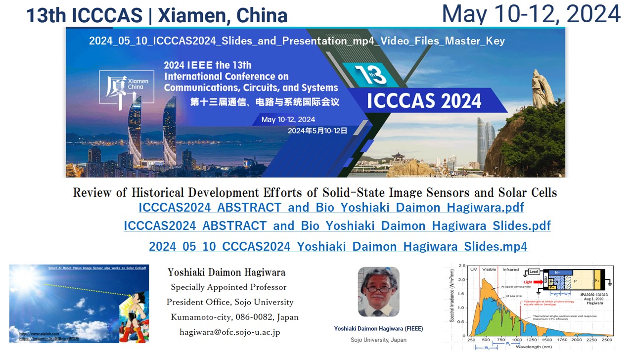
2024_05_10_ICCCAS2024_Slides_and_Presentation_mp4_Video_Files_by_Yoshiaki_Daimon_Hagiwara.pdf
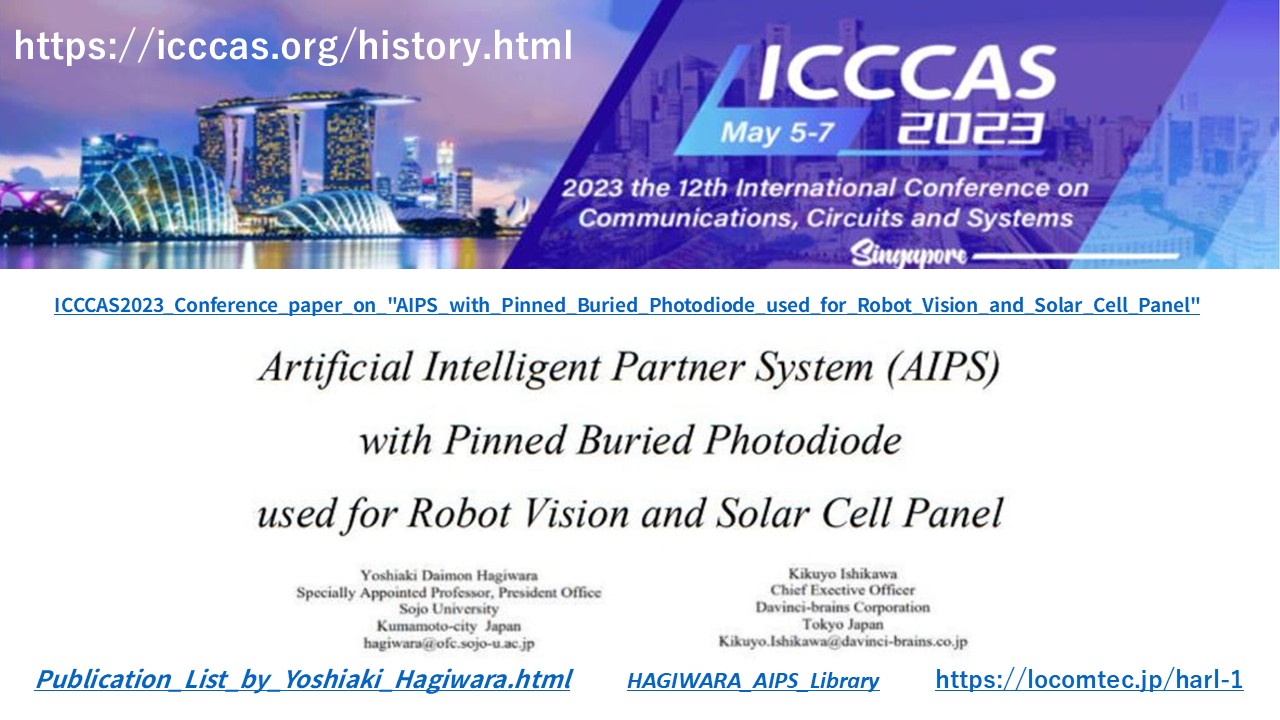
ICCCAS2023_Conference_paper_on_"AIPS_with_Pinned_Buried_Photodiode_used_for_Robot_Vision_and_Solar_Cell_Panel"
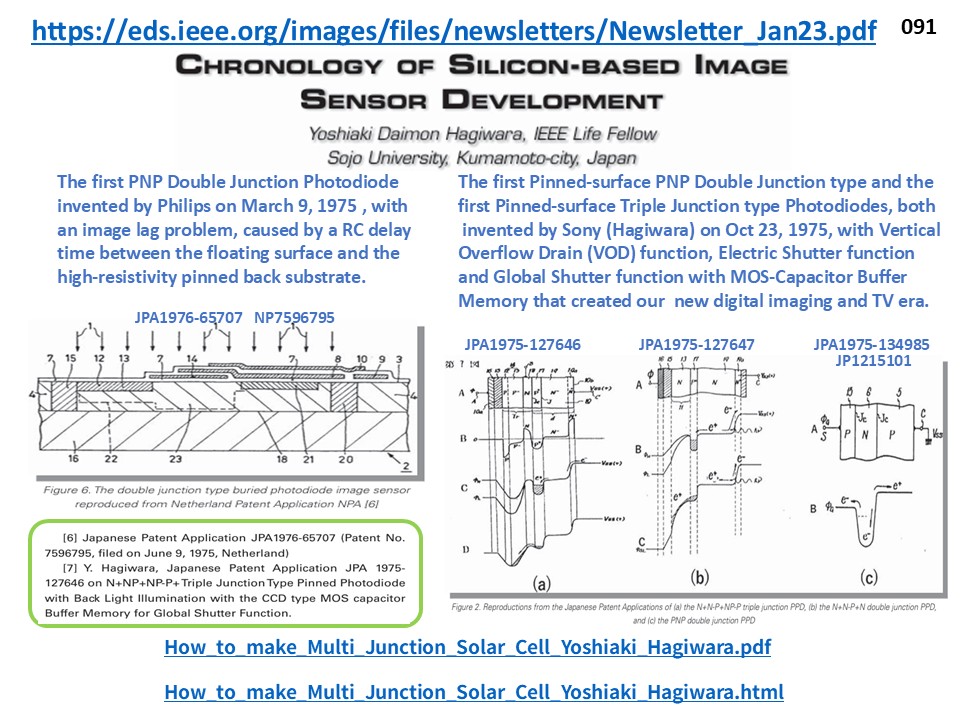
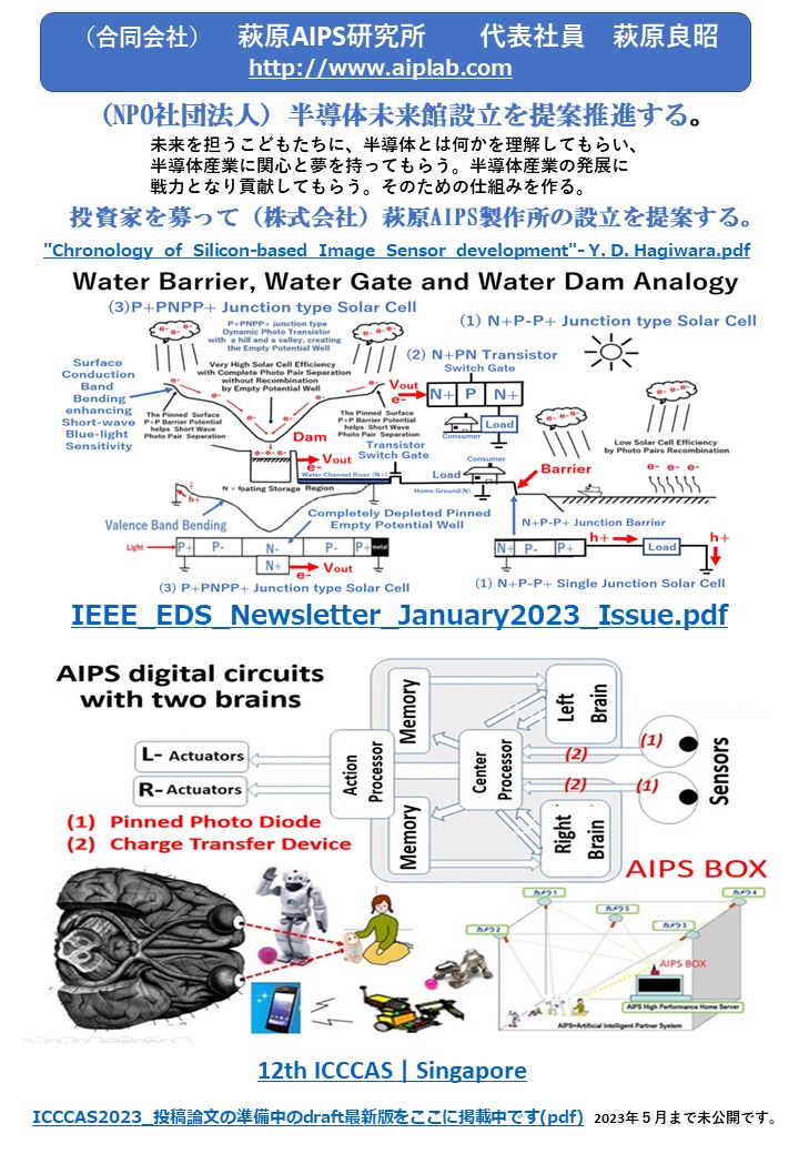
"Chronology_of_Silicon-based_Image_Sensor_development"- Y. D. Hagiwara.pdf
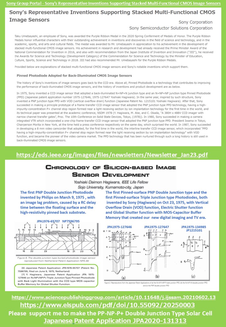
https://eds.ieee.org/images/files/newsletters/Newsletter_Jan23.pdf
IEEE_EDS_Newsletter_January2023_Issue.pdf
https://eds.ieee.org/publications/eds-newsletter
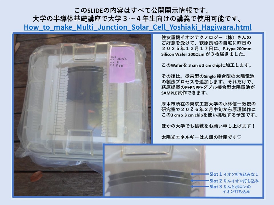
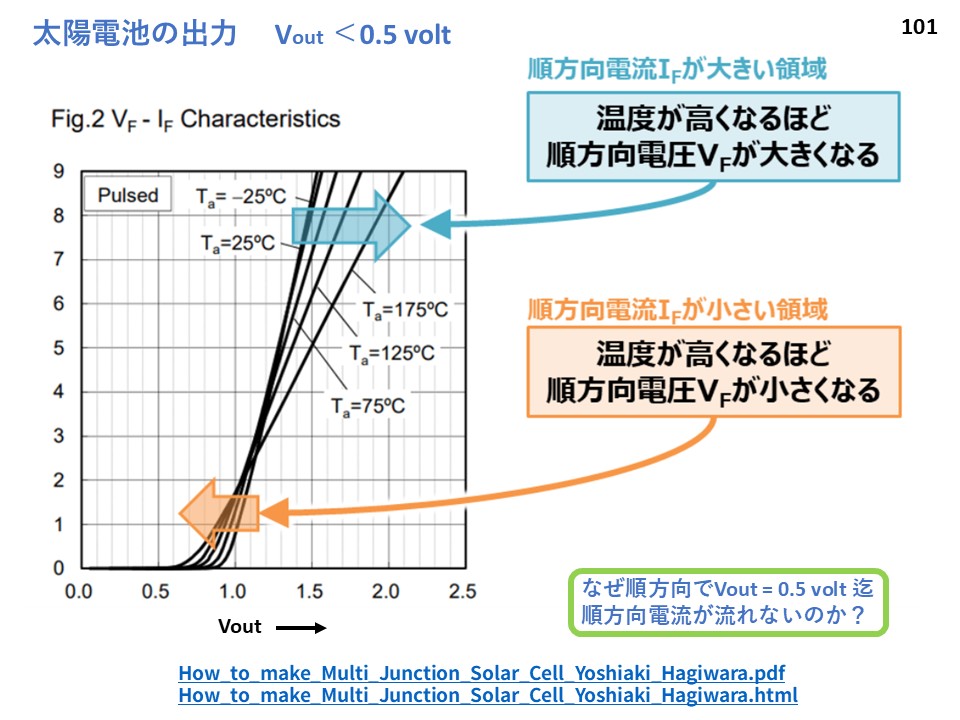
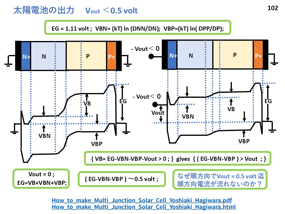
How_to_make_Multi_Junction_Solar_Cell_Yoshiaki_Hagiwara_91.pdf
How_to_make_Multi_Junction_Solar_Cell_Yoshiaki_Hagiwara_2026_01_18.pdf
How_to_make_Multi_Junction_Solar_Cell_Yoshiaki_Hagiwara.pdf
Next_Slide
How_to_make_Multi_Junction_Solar_Cell_Yoshiaki_Hagiwara_67.pdf
How_to_make_Multi_Junction_Solar_Cell_Yoshiaki_Hagiwara_100.pdf
How_to_make_Multi_Junction_Solar_Cell_Yoshiaki_Hagiwara_101.pdf
How_to_make_Multi_Junction_Solar_Cell_Yoshiaki_Hagiwara_102.pdf
How_to_make_Multi_Junction_Solar_Cell_Yoshiaki_Hagiwara.pdf
How_to_make_Multi_Junction_Solar_Cell_Yoshiaki_Hagiwara.html
Ground_Surface_Double_Junction_type_Solar_Cell_Yoshiaki_Hagiwara_AIPS.html
The_Truth_Shall_Make_You_Free.pdf
2026_08_01_ICDIS2026.pdf
ICDIS2026
Dr. Yoshiaki Hagiwara is a key note speaker in ICDIS2026
2026_07_01_ICCCAS2026.pdf
ICCCAS2026
Dr. Yoshiaki Hagiwara is an invited speaker in ICCCAS2026
2025_05_23_ICCCAS2025_Yoshiaki_Daimon_Hagiwara_Wuhan_China_Slides.pdf
2025_05_23_ICCCAS2025_Yoshiaki_Daimon_Hagiwara_Wuhan_China_TEXT.pdf
2025_05_23_ICCCAS2025_Yoshiaki_Daimon_Hagiwara_Wuhan_China.mp4.
ESP2025_05_12_Image_Sensor_with_Built-in_Solar_Cell_Structure_by_Yoshiaki_Daimon_Hagiwara.pdf
https://pdf.elspublishing.com/paper/journal/open/ESP/2025/esp20250003.pdf
2024_05_10_ICCCAS2024_Slides_and_Presentation_mp4_Video_Files_by_Yoshiaki_Daimon_Hagiwara.pdf
ICCCAS2023_Conference_paper_on_"AIPS_with_Pinned_Buried_Photodiode_used_for_Robot_Vision_and_Solar_Cell_Panel"
"Chronology_of_Silicon-based_Image_Sensor_development"- Y. D. Hagiwara.pdf
https://eds.ieee.org/images/files/newsletters/Newsletter_Jan23.pdf
IEEE_EDS_Newsletter_January2023_Issue.pdf
https://eds.ieee.org/publications/eds-newsletter
How_to_make_Multi_Junction_Solar_Cell_Yoshiaki_Hagiwara_91.pdf
How_to_make_Multi_Junction_Solar_Cell_Yoshiaki_Hagiwara.pdf
How_to_make_Multi_Junction_Solar_Cell_Yoshiaki_Hagiwara.html
Ground_Surface_Double_Junction_type_Solar_Cell_Yoshiaki_Hagiwara_AIPS.html
The_Truth_Shall_Make_You_Free.pdf
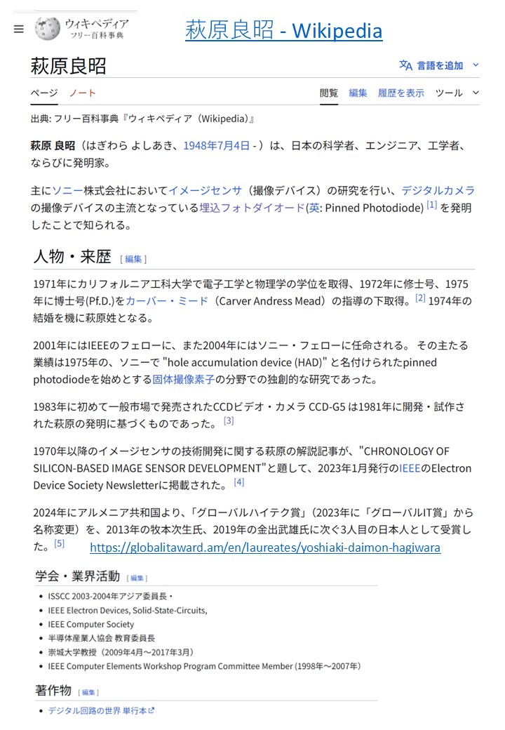
P2025_11_27_Wikipedia_Hagiwara_Yoshiaki.pdf
SSIS_半導体講座2022_イメージセンサ_賢い電子の目_萩原良昭講師.pdf
Concept of Electron Fog Yoshiaki Hagiwara.pdf
How_to_make_Multi_Junction_Solar_Cell_Yoshiaki_Hagiwara.html
https://pdf.elspublishing.com/paper/journal/open/ESP/2025/esp20250003.pdf
How_to_make_Multi_Junction_Solar_Cell_Yoshiaki_Hagiwara.html
Armenia_Global_High_Tech_Award_2024_to_Hagiwara_Daimon_Yoshiaki_AIPS
Hagiwara_履歴_2023_03_24.pdf
Bio_and_List_of_Publications_Yoshiaki_Daimon_Hagiwara.pdf
Page005 半導体未来館(マンガ館)設立の提案_LOCOMTEC社萩原aips研究所.pdf
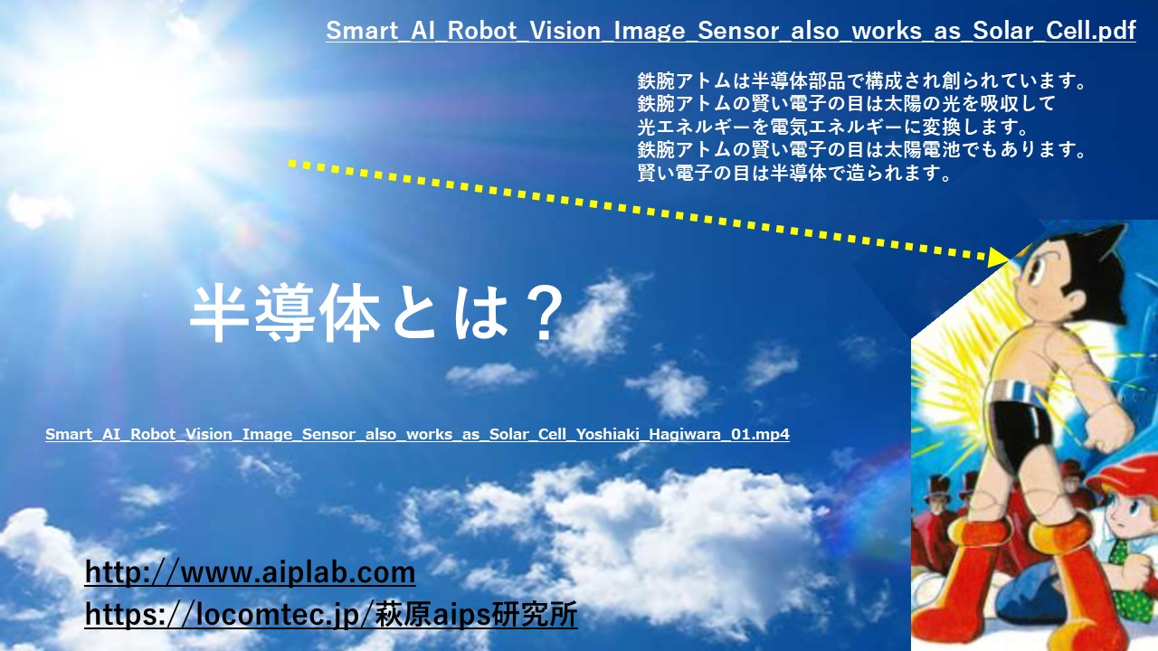
Smart_AI_Robot_Vision_Image_Sensor_also_works_as_Solar_Cell_Yoshiaki_Hagiwara.pdf
Smart_AI_Robot_Vision_Image_Sensor_also_works_as_Solar_Cell_Yoshiaki_Hagiwara.pdf
Smart_AI_Robot_Vision_Image_Sensor_also_works_as_Solar_Cell_Yoshiaki_Hagiwara_01.mp4
Concept_of_Electron_Fog_amd_Solar_Cell_Band_Diagram.pdf
Electrostatic_Potential_Analysis_of_the_Pinned-surface_P+PNPsubP+_Double_Junction_Photodiode.pdf
合同会社_LOCOMOTEC_萩原AIPS研究所
半導体未来館/Semiconductor Future Musium(こどもマンガ館/KID Cartoon Theatre)
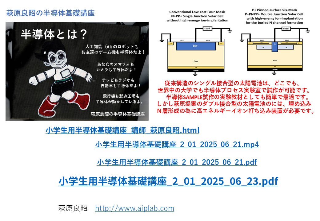
小学生用半導体基礎講座_講師_萩原良昭.html
電子デバイス産業新聞(ID=13645)記事「ソニーの快男児、萩原良昭氏は新世代の鉄腕アトムを作る!」
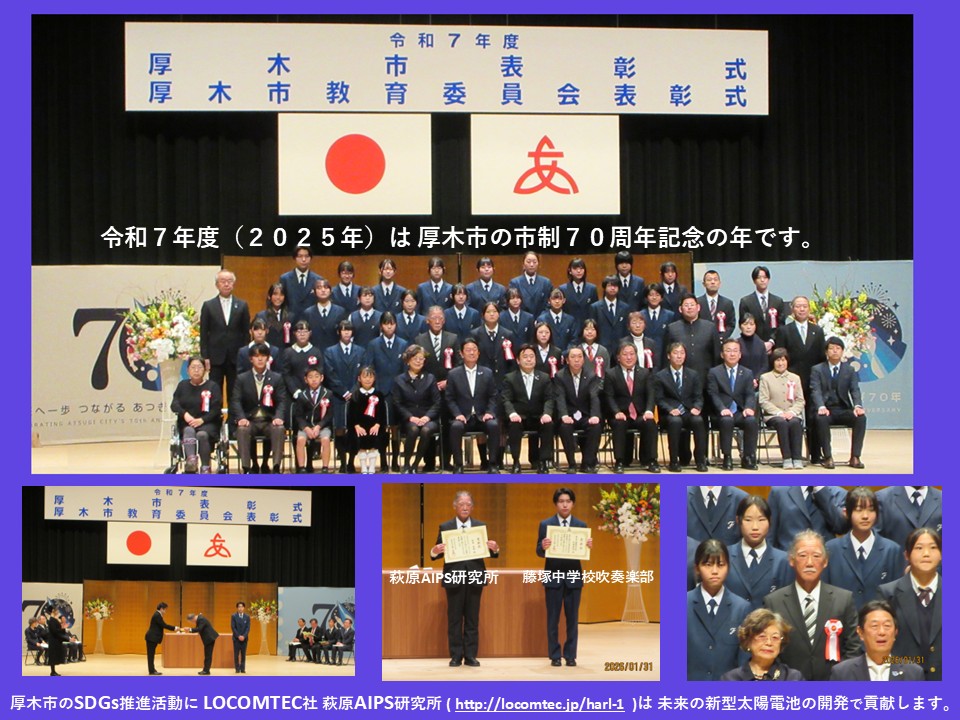
2025_03_03_厚木市発SDGs支援団体_合同会社LOOMTEC社_AIPS萩原研究所の夢を実現に応援をお願いもうしあげます.pdf
合同会社 LOCOMTEC 萩原AIPS研究所のご紹介です
https://locomtec.jp/萩原aips研究所
合同会社LOOMTEC社_AIPS萩原研究所の夢を実現に応援をお願いもうしあげます.pdf
Introduction_to_the_SDGs_activity_in_LOCOMTEC_Hagiwara_AIPS_Lab_in_Atsuigi_city_Japan
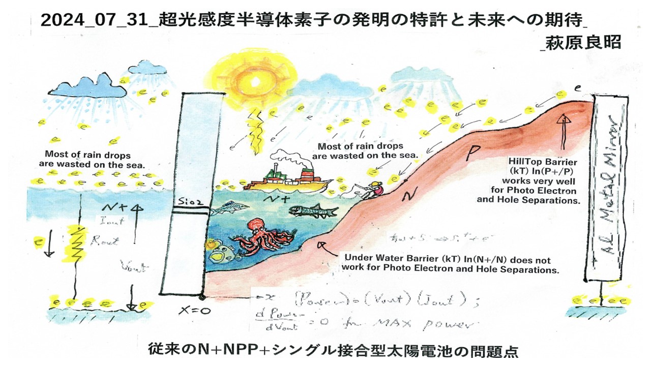
超光感度半導体受光素子を太陽電池に使う事に挑戦します_萩原良昭.pdf
C2025_02_23_シングルPN接合型太陽電池では空乏層幅は最大2μmが限界である事が簡単な計算で求まる_萩原良昭.pdf
C2025_02_22_シングルPN接合型太陽電池では空乏層幅は最大2μmが限界である事が簡単な計算で求まる_萩原良昭.pdf
半導体未来館(マンガ館)のご紹介です
SONYのHADセンサー(Pinned_Photodiode)ダブル接合型太陽電池の提案.pdf
Publication_List_by_Yoshiaki_Hagiwara.html
https://locomtec.com/小学生のための半導体講座/
小学生用半導体基礎講座_講師_萩原良昭.html
小学生用半導体基礎講座_2_01_2025_06_21.pdf
小学生用半導体基礎講座_2_01_2025_06_23.pdf
Page006 Publication_List_by_Yoshiaki_Hagiwara.html
Backups of Past AIPS Homepages.html
半導体未来館の設立のご提案です_萩原良昭.pdf
Sony_Image_Sensor_Story_by_Yoshiaki_Hagiwara.pdf
受光表面の電位は浮遊状態でflatであるSingle接合太陽電池の問題点.html
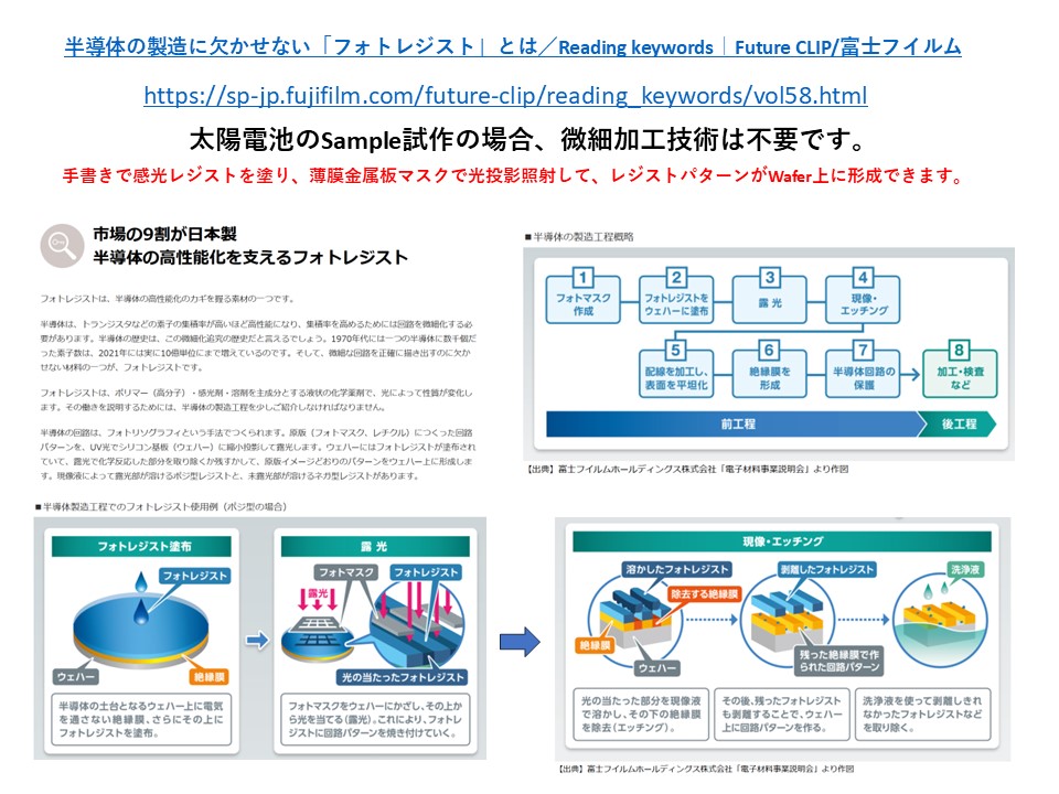
2024_05_日経エレクトニックス_ペロブスカイトのお株を奪うシリコン太陽電池.pdf
従来のN+NPP+シングル接合型のSolar_Cellの問題点.pdf
Pinned_Photodiode_type_Solar_Cell_See_JPA1975_131313_and_JP6828108.html
超光感度半導体素子の発明の特許と未来への期待_萩原良昭.html
日本の産業のコメとして戦略的に重要な半導体電子部品の基本知識.html
P+PNPP+ダブル接合_Pinned_Photodiode型太陽電池の提案_萩原良昭.html
半導体とは?萩原良昭.html
萩原良昭講師の半導体教育講座.html
Introduction_to_the_SDGs_activity_in_LOCOMTEC_Hagiwara_AIPS_Lab_in_Atsuigi_city_Japan
超光感度半導体受光素子を太陽電池に使う事に挑戦します_萩原良昭.pdf
C2025_02_23_シングルPN接合型太陽電池では空乏層幅は最大2μmが限界である事が簡単な計算で求まる_萩原良昭.pdf
C2025_02_22_シングルPN接合型太陽電池では空乏層幅は最大2μmが限界である事が簡単な計算で求まる_萩原良昭.pdf
半導体未来館(マンガ館)のご紹介です
SONYのHADセンサー(Pinned_Photodiode)ダブル接合型太陽電池の提案.pdf
Publication_List_by_Yoshiaki_Hagiwara.html
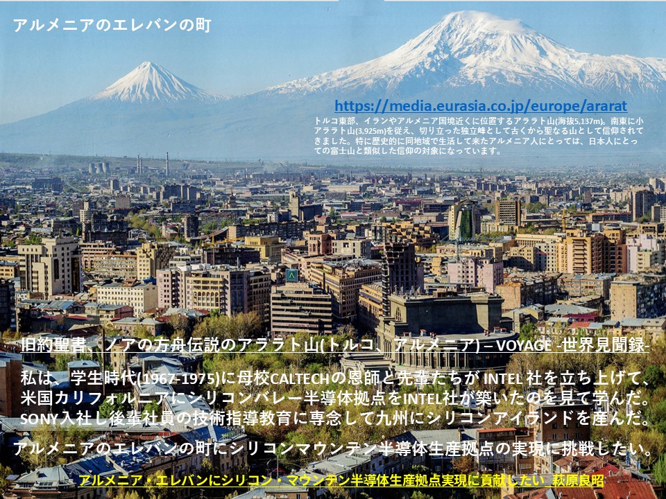
アルメニア・エレバンにシリコン・マウンテン半導体生産拠点実現に貢献したい_萩原良昭
2025_08_01_Intel_made_Silicon_Valey_while_Sony_made_Silicon_Island_and_Armenia_for_Silcion_Mountain.pdf
Publication_List_by_Yoshiaki_Hagiwara.html
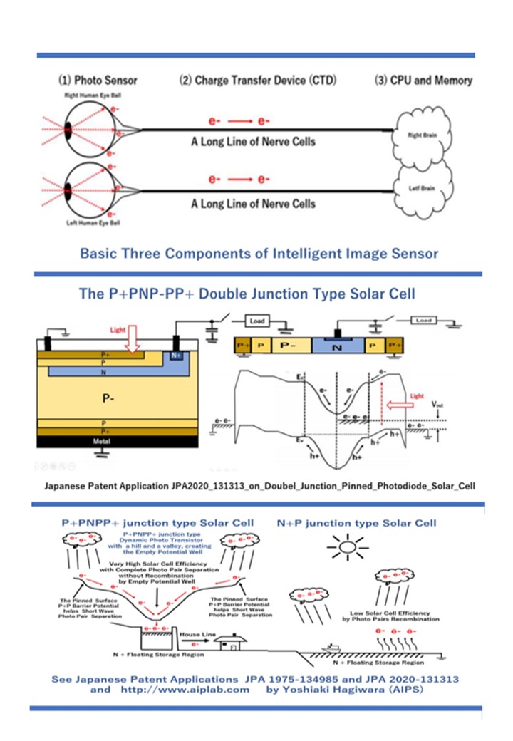
Semiconductor_Device_Physics_of_Pinned_Surface_PNP_Double_Junction_Solar_Cell.pdf
2025_08_13_SONY Bipolar Transistor P+PNPP+ Double Junction type Solar Cell.pdf
C2025_08_13.c )....Doping Profile ( G002.html ) ....Potential Profile ( V001.html )
DOPE(X) for RN=0.5.html ....V(X) for RN=0.5.html
2025_08_13_SONY Bipolar Transistor P+PNPP+ Double Junction type Solar Cell.pdf
C2025_08_13.c )....Doping Profile ( G002.html ) ....Potential Profile ( V001.html )
DOPE(X) for RN=0.5.html ....V(X) for RN=0.5.html
2025_08_13_SONY Bipolar Transistor P+PNPP+ Double Junction type Solar Cell.pdf
2025_07_10_真空管とBipolar_Transistorの構造と動作の相違_萩原良昭.pdf
2025年7月2日(水)朝のつぶやき_萩原良昭.pdf
2025年7月6日(日)朝のつぶやき_萩原良昭.pdf
2025年7月7日(月)朝のつぶやき_萩原良昭.pdf
2025年7月7日(月)朝のつぶやき_萩原良昭.mp4
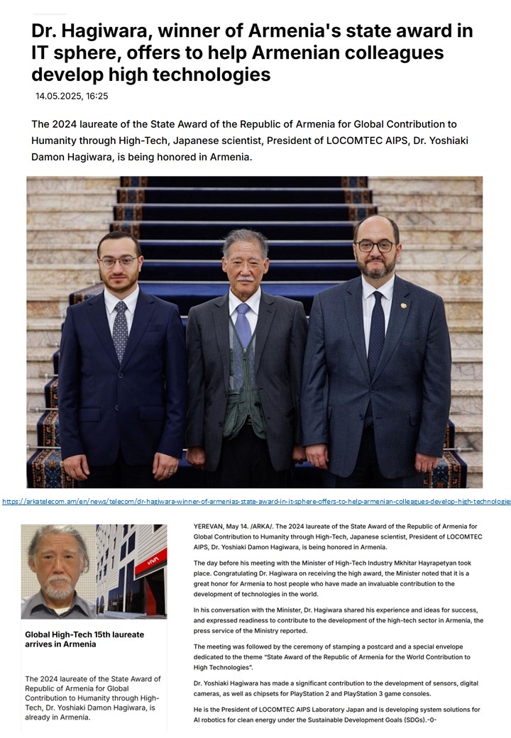
2025-06-26_Armenia_State_Global_High_Technology_Award_2014_Yoshiaki_Daimon_Hagiwara_A.pdf
2025-06-26_Armenia_State_Global_High_Technology_Award_2014_Yoshiaki_Daimon_Hagiwara_B.pdf
2025_07_08_Depletion_Width_WD_of_Siliocn_Single_NP_Junction_Solar_Cell_Yoshiaki_Hagiwara_AIPS.pdf
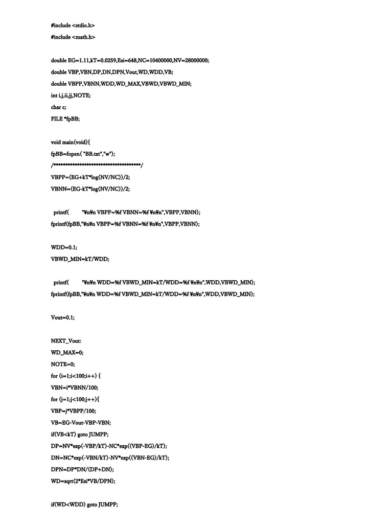
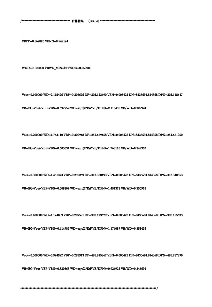
C2025_07_08_Output_Yoshiaki_Hagiwara_AIPS.txt
C2025_07_08_Yoshiaki_Hagiwara_AIPS.txt
2025_06_30_Bipolar_Transistor_P+PNPP+_Double_Junction_Type_Solar_Cell_by_Yoshiaki_Hagiwara_Daimon_August_01_2020.pdf
2025_06_30_Bipolar_Transistor_P+PNPP+_Double_Junction_Type_Solar_Cell_by_Yoshiaki_Hagiwara_Daimon_August_01_2020.mp4
Slide001A/JPG
Slide002A/JPG
Slide001/JPG
Slide002/JPG
Slide003/JPG
Page007 電子デバイス産業新聞(ID=5331)記事(2020.11.13)「鉄腕アトムを創りたい」という男が画像の新世界を切り開く」
電子デバイス産業新聞(ID=13645)記事(2025.1.10)「ソニーの快男児、萩原良昭氏は新世代の鉄腕アトムを作る!」
2025_03_03_厚木市発SDGs支援団体_合同会社LOOMTEC社_AIPS萩原研究所の夢を実現に応援をお願いもうしあげます.pdf
電子デバイス産業新聞2025年1月10日記事「ソニーの快男児、萩原良昭氏は新世代の鉄腕アトムを作る!」
2025_03_03_厚木市発SDGs支援団体_合同会社LOOMTEC社_AIPS萩原研究所の夢を実現に応援をお願いもうしあげます.pdf
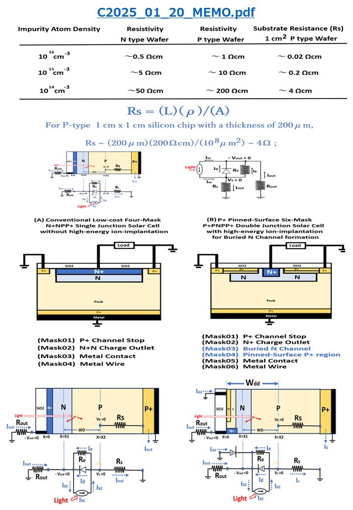
Page008 C2025_01_20_Memo_Solar_Cell.pdf
JPA2020_131313_Bipoalr_Transistor_type_Solar_Cell_by_Yoshiaki_Hagiwrar_2025_06_26.pdf
C2025_01_23_Memo.pdf
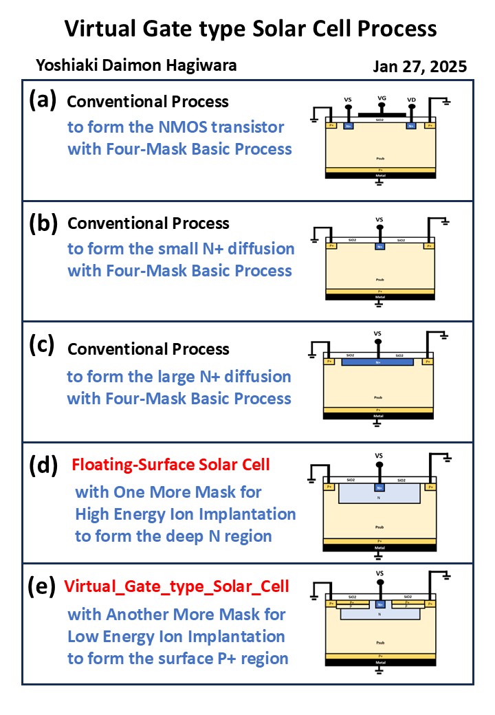
Virtual_Gate_type_Solar_Cell_Process_by_Yoshiaki_Daimon_Hagiwara.pdf
2025_02_11_良昭のひとりごと.mp4
2025_02_13_LOCOMTEC_萩原AIPS研究所の活動紹介.pdf
2025_02_13_LOCOMTEC_萩原AIPS研究所の活動紹介.mp4
C2025_02_23_シングルPN接合型太陽電池では空乏層幅は最大2μmが限界である事が簡単な計算で求まる_萩原良昭.pdf
C2025_02_22_シングルPN接合型太陽電池では空乏層幅は最大2μmが限界である事が簡単な計算で求まる_萩原良昭.pdf
Pinned_Surface_Completely_Depleted_Buried_Channel_Double_Junction_type_Solar_Cell.pdf
Page009 Slide001A/JPG
Slide002A/JPG
2025-06-26_Armenia_State_Global_High_Technology_Award_2014_Yoshiaki_Daimon_Hagiwara_A.pdf
2025-06-26_Armenia_State_Global_High_Technology_Award_2014_Yoshiaki_Daimon_Hagiwara_B.pdf
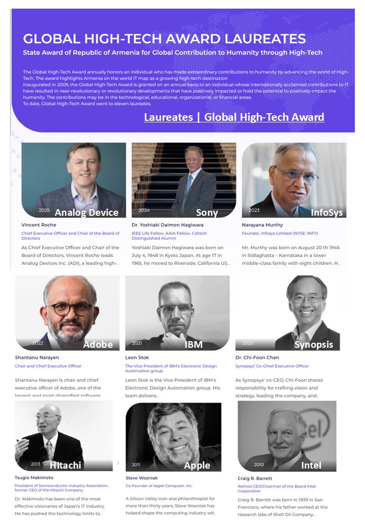
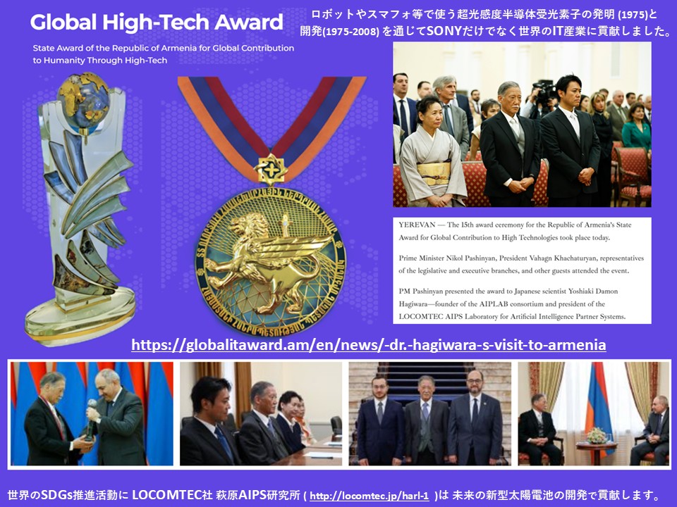
Global_High_Technology_Award_2024_in_Yerevan_Armenia_to_Yoshiaki_Daimon_Hagiwara_on_May_14_2025a.pdf
Global_High_Technology_Award_2024_in_Yerevan_Armenia_to_Yoshiaki_Daimon_Hagiwara_on_May_14_2025.pdf
2025_05_14_Yoshiaki_Daimon_Hagiwara_recieved_Armenia_State_Global_High_Technology_Award_2024_in_Yerevan_Armenia.pdf
https://silicon-mountains.org/
https://armenpress.am/en/article/1219532
https://www.aysor.am/en/news/2025/05/10/Global%20High-Tech/2397167
https://armenpress.am/en/article/1219532
https://massispost.com/2025/05/yoshiaki-damon-hagiwara-receives-armenias-state-award-for-global-contribution-to-high-technologies/
2025_05_15_Yoshiaki_Hagiwara_in_Silicon_Mountains_Lori_2025_in_Yerevan_and_in_ISSCC2013_Siliocn_Vally_in_San_Francisco.pdf
2025_05_23_ICCCAS2025_Yoshiaki_Daimon_Hagiwara_Wuhan_China.html
2025_06_10_Hagiwara is the winner of the Armenia State Global High Technology Award 2024.pdf
https://www.1lurer.am/en/2025/05/15/Japanese-scientist-Yoshiaki-Damon-Hagiwara-awarded-Armenian-State-Prize-for-his-global-contribution/1313811
Armenia_State_Global_High_Technology_Award_2024_Yoshiaki_Daimon_Hagiwara_D.pdf
2025_05_15_Yoshiaki_Hagiwara_Armenia_Global_High_Technology_Award_2024_Winner
New Armenian stamp depicts Japanese scientist Yoshiaki Hagiwara
Armenia_State_Global_High_Technology_Award_2024_Yoshiaki_Daimon_Hagiwara.pdf
Armenia_State_Global_High_Technology_Award_2024_Yoshiaki_Daimon_Hagiwara_ENG.mp4
Armenia_State_Global_High_Technology_Award_2024_Yoshiaki_Daimon_Hagiwara_JPN.mp4
2025_10_09_九州半導体展メモ_萩原良昭.mp4
2025_10_10_これからは日本全体の半導体の発展期待_萩原良昭.mp4
2025_10_13_Memo_日本半導体の過去現在未来_萩原良昭
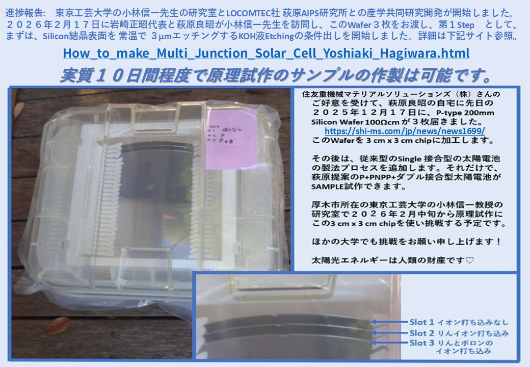
2026_02_17_How_to_make_Multi_Junction_Solar_Cell_Yoshiaki_Hagiwara.pdf
How_to_make_Multi_Junction_Solar_Cell_Yoshiaki_Hagiwara.html
2026_02_19_ダブル接合型太陽電池の提案_萩原良昭.pdf
2026_02_12_How_to_make_Multi_Junction_Solar_Cell_Yoshiaki_Hagiwara_Top.pdf
"Chronology_of_Silicon-based_Image_Sensor_development"- Y. D. Hagiwara.pdf
https://eds.ieee.org/images/files/newsletters/Newsletter_Jan23.pdf
IEEE_EDS_Newsletter_January2023_Issue.pdf
https://eds.ieee.org/publications/eds-newsletter
How_to_make_Multi_Junction_Solar_Cell_Yoshiaki_Hagiwara_91.pdf
Please_support_me_to_make_the_PP-NP-P+_double_junction_solar_cell.pdf
2026_07_01_ICCCAS2026.pdf
ICCCAS2026
Dr. Yoshiaki Hagiwara is an invited speaker in ICCCAS2026
Publication_List_by_Yoshiaki_Hagiwara.html
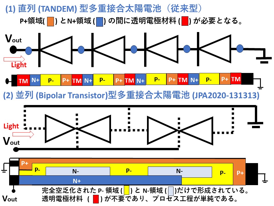
2026_03_23_The_Difference_between_Hagiwara_JPA2020_131313_Multi_junction_Solar_Cell_and_Conventional_Tandem_Solar_cell.pdf
Mathematics_and_Physics_of_Semiconductor_Devices_by_Yoshiaki_Hagiwara_AIPS.pdf
Yoshiaki_Hagiwara_AIPS_Donation_Guide.pdf
Conribution_to_Global_High_Technology_Yoshiaki_Daimon_Hagiwara_AIPS.pdf
Conribution_to_Global_High_Technology_Yoshiaki_Daimon_Hagiwara_AIPS_1.pdf
Conribution_to_Global_High_Technology_Yoshiaki_Daimon_Hagiwara_AIPS_2.pdf
Publication_List_by_Yoshiaki_Hagiwara.html
小学生用半導体基礎講座_講師_萩原良昭.html
小学生用半導体基礎講座_1_10_2025_05_28.pdf
2025_09_10_SONY Bipolar Transistor P+PNPP+ Double Junction type Solar Cell.pdf
C2025_08_13.c )....Doping Profile ( G002.html ) ....Potential Profile ( V001.html )
DOPE(X) for RN=0.5.html ....V(X) for RN=0.5.html
Light Sensitivity Measurement Circuit_used_in_SSDM1978_SONY_and_IEMD1984_KODAK.pdf
Publication_List_by_Yoshiaki_Hagiwara.html
P2025_ESP_Journal_Image_Sensor_with_Built-in_Solar_Cell_Structure.pdf
合同会社LOCOMTEC/萩原aips研究所
https://www.sciencepublishinggroup.com/article/10.11648/j.ijssam.20210602.13
https://eds.ieee.org/images/files/newsletters/Newsletter_Jan23.pdf ( See pp.22-31 )
https://www.elspub.com/pdf/doi/10.55092/20250003
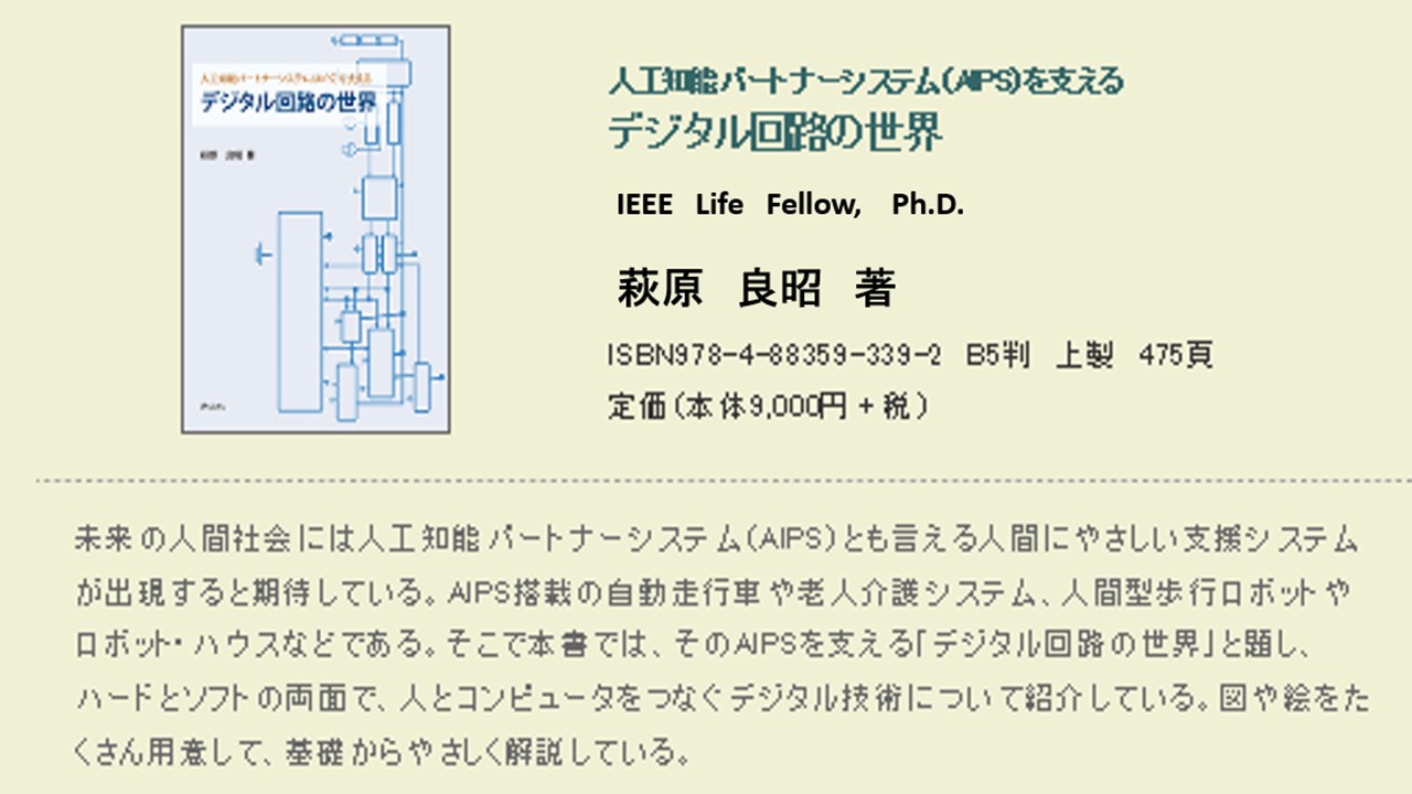
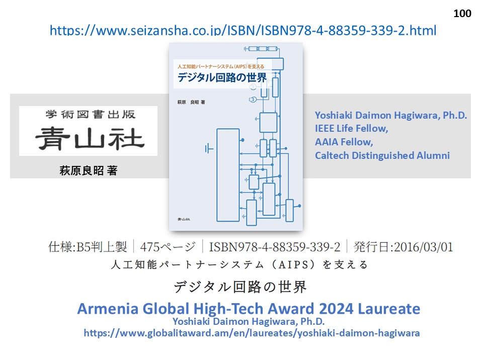
https://www.seizansha.co.jp/ISBN/ISBN978-4-88359-339-2.html
Mathematics_and_Physics_of_Semiconductor_Devices_by_Yoshiaki_Hagiwara_AIPS_Top.pdf
The_World_of_Digital_Circuits_for_AI_Robot_Applications_by_Yoshiaki_Daimon_Hagiwara_AIPS_in_Japanese.html
The_World_of_Digital_Circuits_for_AI_Robot_Applications_by_Yoshiaki_Daimon_Hagiwara_AIPS_in_English.html
https://www.ssis.or.jp hagiwara(@)ssis.or.jp
http://www.aiplab.com hagiwara(@)aiplab.com
https://locomtec.jp/萩原aips研究所
https://ja.wikipedia.org/wiki/萩原良昭
https://en.wikipedia.org/wiki/Yoshiaki_Hagiwara
Publication_List_by_Yoshiaki_Hagiwara.html
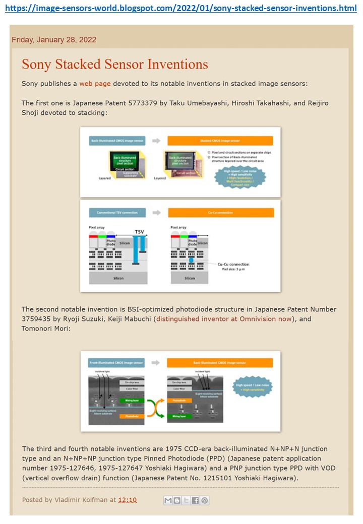
Sony_Stacked_Sensor_Inventions.pdf
https://www.sangyo-times.jp/article.aspx?ID=5331 Sangyo-Times.jp/article_ID=5331_(PDF) Sangyo-Times.jp/article_ID=5331_(html) Pinned_Buried_Photodiode_with_Electrical_Shutter_Function.pdf Hagiwara_履歴_2023_03_24.pdf
Bio_and_List_of_Publications_Yoshiaki_Daimon_Hagiwara.pdf
Publication_List_by_Yoshiaki_Hagiwara.html
HOP_応援募金活動報告_応援ありがとうございます_萩原良昭.html
Locomtec.jp/萩原aips研究所のご案内
Publication_List_by_Yoshiaki_Hagiwara.html
Introduction to the world of Super Light Sensitive Image Sensor and Solar Cell
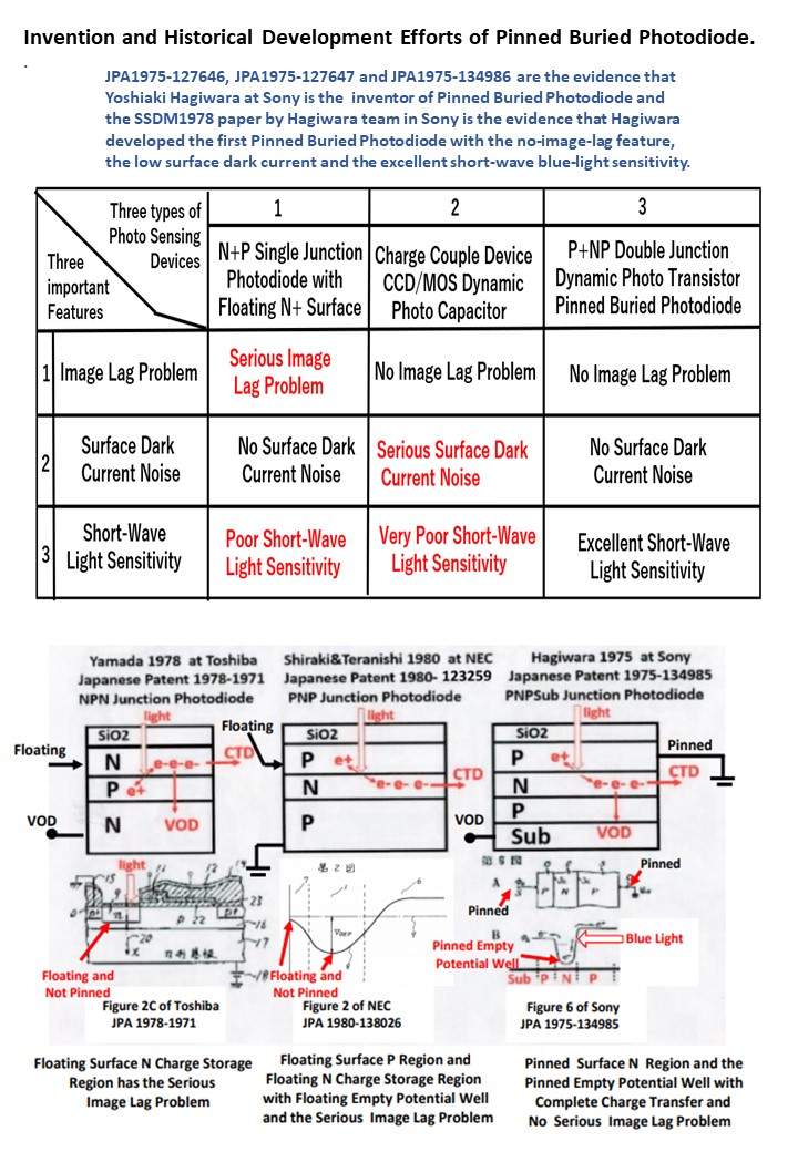
The_Respectful_Words_of_Kawana_Yoshiyuki_on_Pinned_Photodiode.pdf Invention_an_Historical_Developmen_Efforts_of_Pinne_Burie_Photodiode.pdf Hagiwara_AIPS_Laboratory.html
Publication_List_by_Yoshiaki_Hagiwara.html
The_World_of_Digital_Circuits_for_AI_Robot_Applications_by_Yoshiaki_Daimon_Hagiwara_AIPS.pdf
The_World_of_Digital_Circuits_for_AI_Robot_Applications_by_Yoshiaki_Daimon_Hagiwara_AIPS_in_Japanese.html
The_World_of_Digital_Circuits_for_AI_Robot_Applications_by_Yoshiaki_Daimon_Hagiwara_AIPS_in_English.html
https://www.sangyo-times.jp/article.aspx?ID=5331 http://www.aiplab.com/Hagiwara_invented_PPD_and_Sony_HAD_in_1975.pdf https://www.sony.com/ja/SonyInfo/News/notice/20200626/ AIPS_Library/AIPS_210123/002_Image_Sensor_Story_by_Hagiwara.pdf The_Truth_Shall_Make_You_Free.pdf AIPS_251013.html AIPS_250912.html AIPS_250624.html AIPS_240822.html AIPS_240309.html AIPS_230316.html AIPS_221231.html AIPS_220823.html AIPS_220131.html AIPS_211226.html AIPS_211206.html AIPS_211107.html AIPS_210929.html AIPS_210906.html AIPS_210811.html AIPS_210404.html AIPS_210301.html AIPS_210217.html AIPS_210215.html AIPS_201209.html AIPS_200627.html AIPS_190925.html AIPS_190712.html AIPS_181129.html AIPS_090628.html 合同会社LOCOMTEC/萩原aips研究所
Publication_List_by_Yoshiaki_Hagiwara.html
https://www.sangyo-times.jp/article.aspx?ID=5331 Sangyo-Times.jp/article_ID=5331_(PDF) Sangyo-Times.jp/article_ID=5331_(html) Pinned_Buried_Photodiode_with_Electrical_Shutter_Function.pdf 2026_02_17_How_to_make_Multi_Junction_Solar_Cell_Yoshiaki_Hagiwara.pdf
How_to_make_Multi_Junction_Solar_Cell_Yoshiaki_Hagiwara.html
2026_02_19_ダブル接合型太陽電池の提案_萩原良昭.pdf
2026_02_12_How_to_make_Multi_Junction_Solar_Cell_Yoshiaki_Hagiwara_Top.pdf
"Chronology_of_Silicon-based_Image_Sensor_development"- Y. D. Hagiwara.pdf
https://eds.ieee.org/images/files/newsletters/Newsletter_Jan23.pdf
IEEE_EDS_Newsletter_January2023_Issue.pdf
https://eds.ieee.org/publications/eds-newsletter
How_to_make_Multi_Junction_Solar_Cell_Yoshiaki_Hagiwara_91.pdf
小学生用半導体基礎講座_講師_萩原良昭.html
小学生用半導体基礎講座_1_10_2025_05_28.pdf
SONYのHADセンサー(Pinned_Photodiode)ダブル接合型太陽電池の提案.pdf
2025_02_13_LOCOMTEC_萩原AIPS研究所の活動紹介.pdf
2025_02_13_LOCOMTEC_萩原AIPS研究所の活動紹介.mp4
超光感度半導体受光素子を太陽電池に使う事に挑戦します_萩原良昭.pdf
C2025_02_23_シングルPN接合型太陽電池では空乏層幅は最大2μmが限界である事が簡単な計算で求まる_萩原良昭.pdf
C2025_02_22_シングルPN接合型太陽電池では空乏層幅は最大2μmが限界である事が簡単な計算で求まる_萩原良昭.pdf
C2025_01_20_Memo_Solar_Cell.pdf
Pinned_Surface_Completely_Depleted_Buried_Channel_Double_Junction_type_Solar_Cell.pdf
SONY(萩原良昭)のLife_Work_夢と挑戦.pdf
2025_02_11_良昭のひとりごと.mp4
C2025_01_23_Memo.pdf
Virtual_Gate_type_Solar_Cell_Process_by_Yoshiaki_Daimon_Hagiwara.pdf
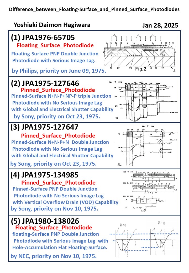
Difference_between_Floating-Surface_and_Pinned_Surface_Photodiodes_by_Yoshiaki_Daimon_Hagiwara.pdf
Bio_and_List_of_Publications_Yoshiaki_Daimon_Hagiwara.pdf
Smart_AI_Robot_Vision_Image_Sensor_also_works_as_Solar_Cell_Yoshiaki_Hagiwara.pdf
Smart_AI_Robot_Vision_Image_Sensor_also_works_as_Solar_Cell_Yoshiaki_Hagiwara_01.mp4
Concept_of_Electron_Fog_amd_Solar_Cell_Band_Diagram.pdf
Electrostatic_Potential_Analysis_of_the_Pinned-surface_P+PNPsubP+_Double_Junction_Photodiode.pdf
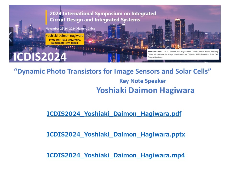
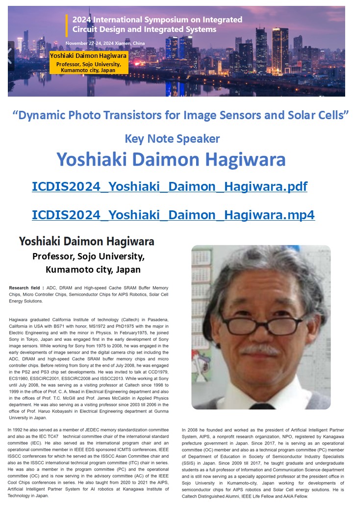
2024_11_22_ICDIS2024_Conference_Slides_Link_Hagiwara.pdf
Locomtec.jp/萩原aips研究所のご案内
Hagiwara_履歴_2023_03_24.pdf
Publication_List_by_Yoshiaki_Hagiwara.html
Hagiwara_履歴_2023_03_24.pdf
2024_11_22_ICDIS2024_Key_Note_Yoshiaki_Daimon_Hagiwara_Sojo_University.pdf
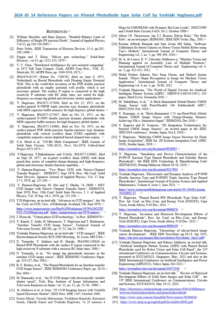
2024_05_14_Reference_Papers_on_Pinned_Photodiode_type_Solar_Cell_by_Yoshiaki_Hagiwara.pdf
P2023_10_20_AIPE2023_Tokyo_Conference_Paper_on_AIPS_with_PBP_for_Robot_Vision_and_Solar_Cell_Panel.pdf
Hagiwara_履歴_2023_03_24.pdf
AIPS_Library_past_file_AIPS_090628_index.html
2024_05_10_ICCCAS2024_Slides_and_Presentation_mp4_Video_Files_by_Yoshiaki_Daimon_Hagiwara.pdf
http://www.icccas.org/
ICCCAS2023_Conference_paper_on_"AIPS_with_Pinned_Buried_Photodiode_used_for_Robot_Vision_and_Solar_Cell_Panel"
"Chronology_of_Silicon-based_Image_Sensor_development"- Y. D. Hagiwara.pdf
https://eds.ieee.org/images/files/newsletters/Newsletter_Jan23.pdf
IEEE_EDS_Newsletter_January2023_Issue.pdf
https://eds.ieee.org/publications/eds-newsletter
2024_04_Publication_List_and_Bio_Yoshiaki_Daimon_Hagiwara.pdf
http://www.aiplab.com/
Evidence_that_Hagiwara_at_Sony_invented_Pinned_Buried_Photodiode_in_1975.pdf
http://www.aiplab.com/
Yoshiaki_Hagiwara_Bio.pdf
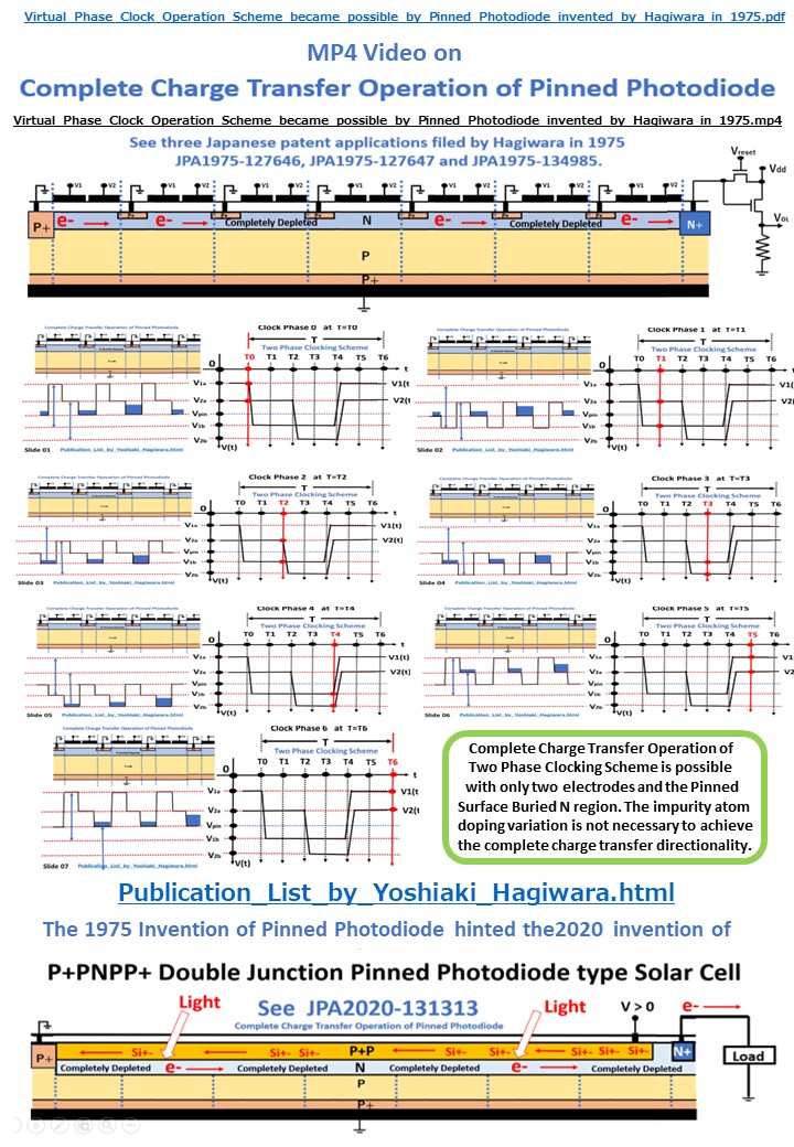
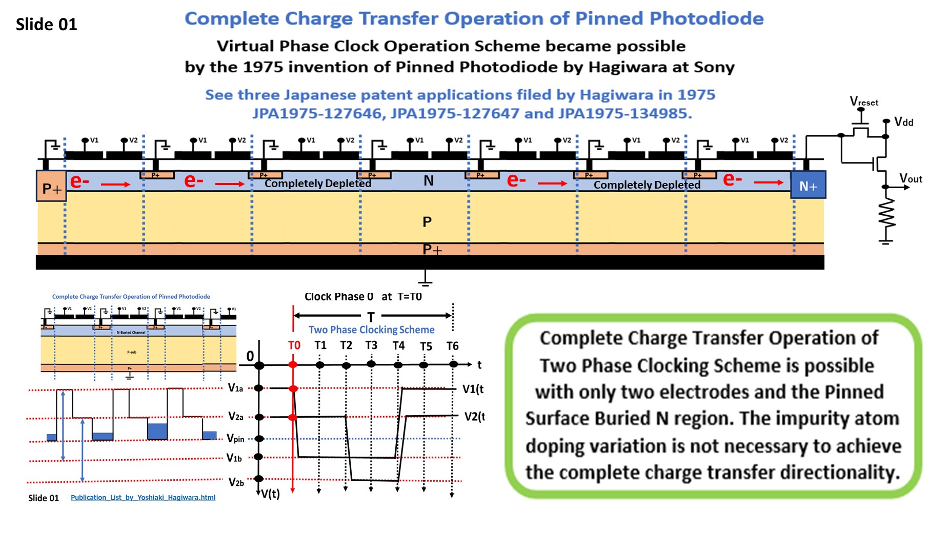
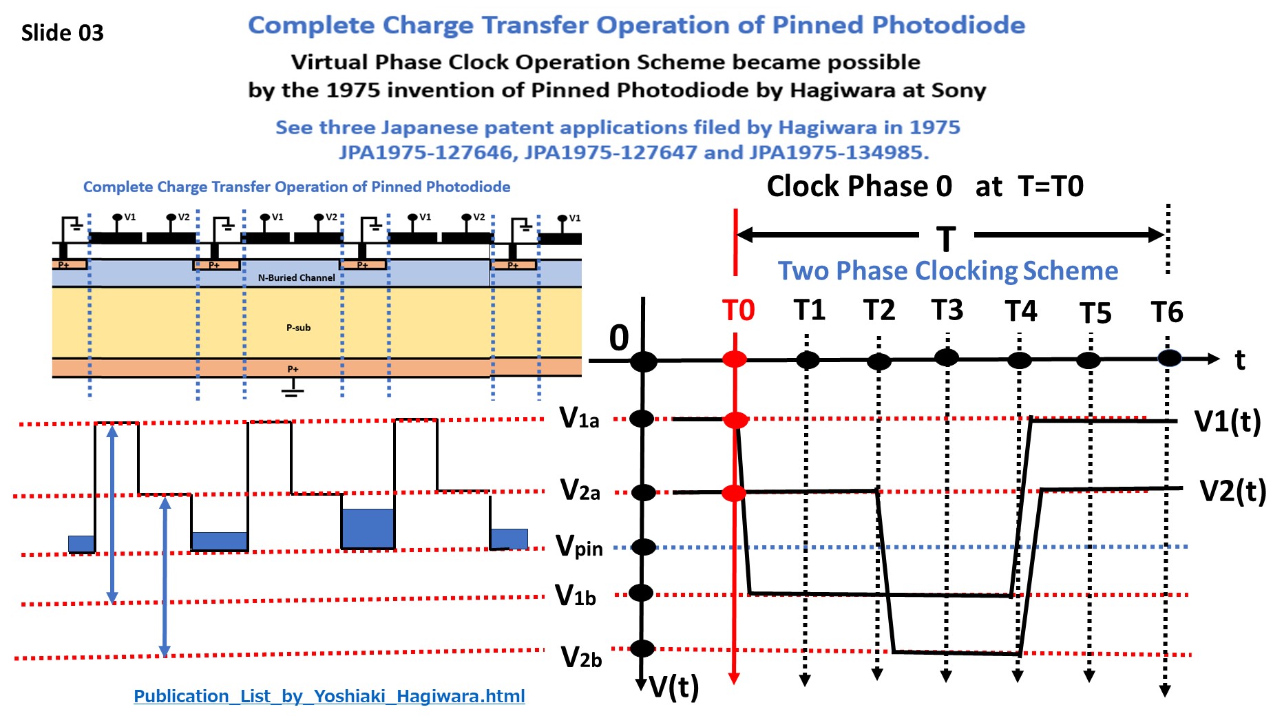
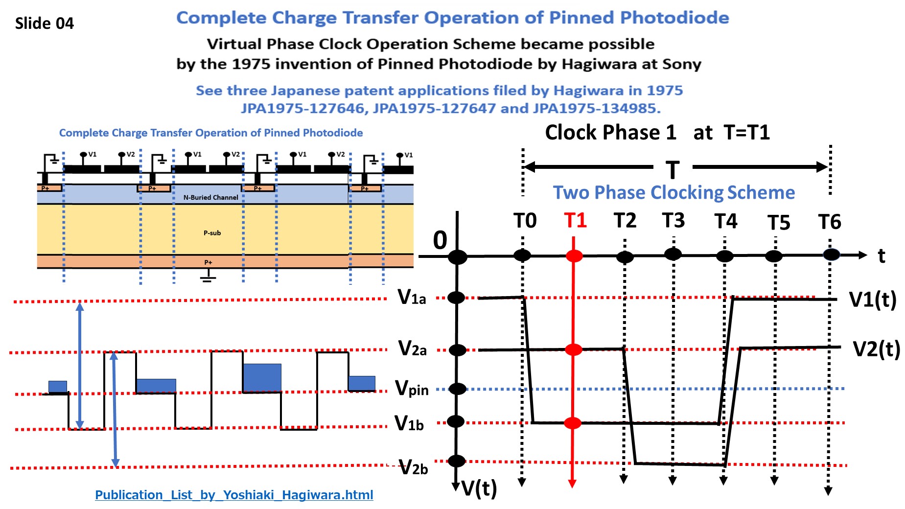
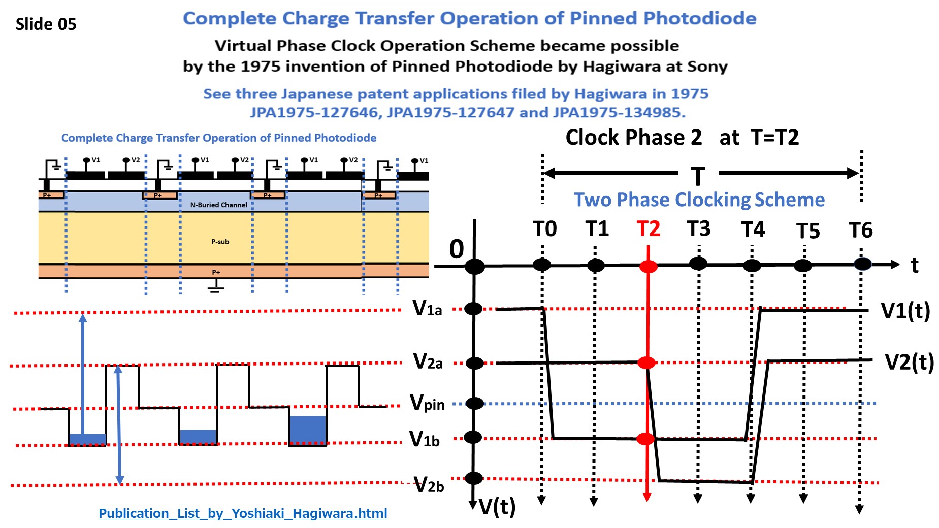
Virtual_Phase_Clock_Operation_Scheme_became_possible
Virtual_Phase_Clock_Operation_Scheme_became_possible
slides_pdf.file
P2019_3DIC2019_Paper_on_3D_Pinned_Photodiode_6_pages.pdf
P2020_EDTM2020_PaperID_3C4_by_Hagiwara_4_pages.pdf
EDTM2020_Paper_on_the P+PN+P Junction Pinned Photodiode and Schottky Barrier Photodiode.html
P2021_IJSSA2021_Paper_20210616_on_Electrostatic_and_Dynamic_Analysis_of_Pinned_Photodiodes.pdf
P2021_IJSSA2021_Paper_20210616_on_Electrostatic_and_Dynamic_Analysis_of_Pinned_Photodiodes.html
ICECET2021_Paper61_html
ICECET2021_Paper75_html
Chronology_of_Silicon_based_Image_Sensor_Development
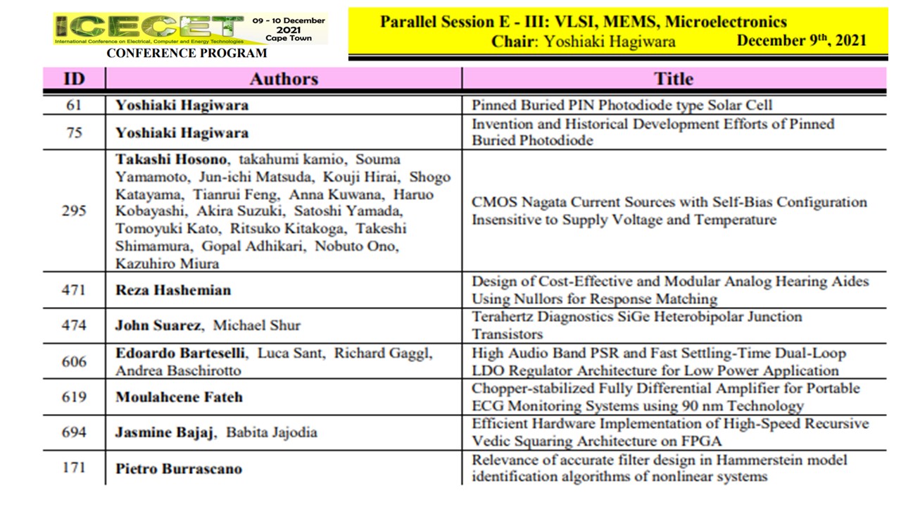
http://www.icecet.com/home http://www.icecet.com/ICECET_Program.pdf ICECET2021_Session_E-III_chaired_by_Yoshiaki_Hagiwara.pdf ICECET2021_Program_Session_E-III.pdf ICECET2021_Paper61_html ICECET2021_Paper75_html http://www.icecet.com/home http://www.icecet.com/ICECET_Program.pdf ICECET2021_Session_E-III_chaired_by_Yoshiaki_Hagiwara.pdf 001A_ICECET2021_Paper061_Pinned Buried PIN Photodiode type Solar Cell.pdf 001B_ICECET2021_acceptance_letter_ID_061.pdf 001C_ICECET 2021_PARTICIPATION_CERTIFICATE_061.pdf 001D_ICECET2021_Paper061_supplement_Process_Flow_of_Pinned_Buried_PIN_Photodiode_type_Solar_Cell_2021_08_14.pdf 002A_ICECET2021_Paper075_Invention and Historical Development Efforts of Pinned Buried Photodiode.pdf 002B_ICECET2021_acceptance_letter_ID_075.pdf 002C_ICECET 2021 PARTICIPATION CERTIFICATE_075.pdf 002D_ICECET2021_Paper075_supplement_The_Evidence_that_Hagiwar_at_Sony_invente_Pinne_Burie_Photodiode_in_1975.pdf 003_ICECET2021_CHAIR_CERTIFICATE_Session_E3.pdf 004_ICECET2001_Session_E-III_Chaired_by_Yoshiaki_Hagiwara.pdf Sony_vs_Loral_Patent_War_1_Reviews.pdf Sony_vs_Loral_Patent_War_2_Supporting_Opinions.pdf E-mail_Communication_on_Sony_Loral_Patent_War_1996.pdf E-mail_communication_with_Albert_san_2018_07_10.pdf HAD_sensor_NEC_SONY_Patent_War.pdf JP1980_138026_NEC_Buried_Photodiode_Patent.pdf JP1978-1971_Toshiba_Yamada_VOD_patent.pdf Sony_vs_Loral_PAtent_War_13_pages.pdf Sony_vs_Loral_Patent_War_53_pages.pdf Image_Sensor_Story_by_Hagiwara.pdf The_evidence_that_Hagiwara_is_the_inventor_of_Pinned_Photodiode_7_pages.pdf Future_of_Image_Sensors_and_Solar_Cells.pdf JP1975-127646_NPNP_triple_junction_Pinned_Photodiode_Patent_32_pages.pdf The_First_Pinned_Photodiode_was_invented_in_1975_by_Yoshiaki_Hagiwar_at_Sony.pdf JP1975-127647_NPN_double_junction_Pinned_Photodiode_Patent_22_pages.pdf JP1975-134985_PNP_double_junction_Pinned_Photodiode_on_Nsub_Patent_7_pages.pdf JP1977-126885_Elecric_Shutter_Clocking_Scheme_by_OFD_Punch_Thru_Action_13_pages.pdf JP2014-135497_Digital_Transformation_Circuit_for_Image_Sensors_29_pages.pdf JP2020_131313_on_Doubel_Junction_Pinned_Photodiode_Solar_Cell_65_Pages.pdf JPA_2020_131313_Japan_Patent_6818208_on_Pinned_Photodiode_type_Solar_Cell_by_Hagiwara.pdf P1978_Pinned_Photodiode_1978_Paper_by_Hagiwara_7_Pages.pdf P1996_Pinned_Photodidoe_used_in_Sony_1980_FT_CCD_Image_Sensor_9_Pages.pdf P2001_ESSCIRC2001_Micro-Electronics_for_Home_Entertainment_11_pages.pdf P2008_ESSCIRC_2008_SOI_Design_in_Cell_Processor_and_Beyond_7_pages.pdf P2013_ISSCC2013_Panel_Talk_25_pages.pdf P2017_CoolChips_Panel_170419_29_pages.pdf P2019_3DIC2019_Paper_on_3D_Pinned_Photodiode_6_pages.pdf P2020_EDTM2020_PaperID_3C4_by_Hagiwara_4_pages.pdf P2021_IJSSA2021_Paper_20210616_on_Electrostatic_and_Dynamic_Analysis_of_Pinned_Photodiodes.pdf ICECET2021_Paper61_html ICECET2021_Paper75_html Chronology_of_Silicon_based_Image_Sensor_Development
Buried_Photodiode_is_not_always_PPD_Hagiwara_Nov_2020.pdf Caltech_1975_PhD_Thesis_Yoshiaki_Daimon_Hagihara.pdf Difference_of_Buried_Photodiode_and_Pinned_Photodiode.pdf E-mail_Communication_on_Sony_Loral_Patent_War_1996.pdf E-mail_communication_with_Albert_and_Yoshi.pdf E-mail_communication_with_Albert_san_2018_07_10.pdf E-mail_communication_with_Albert_san_2018_07_10A.pdf E-mail_communication_with_Albert_san_2018_07_10B.pdf Evidence_that_Hagiwara_is_the_inventor_of_Pinned_Photodiode_2020_10_04a.pdf Evidence_that_Hagiwara_is_the_inventor_of_Pinned_Photodiode_in_Japanese.pdf https://www.seizansha.co.jp/ISBN/ISBN978-4-88359-339-2.html https://www.seizansha.co.jp/ https://www.sangyo-times.jp/article.aspx?ID=5331 Sangyo-Times.jp/article_ID=5331_(PDF) Sangyo-Times.jp/article_ID=5331_(html) Candy_in_the_Heart TOP 010 ,
020 ,
030 ,
040 ,
050 ,
060 ,
070 ,
080 ,
090 ,
100 110 ,
120 ,
130 ,
140 ,
150 ,
160 ,
170 ,
180 ,
190 ,
200 210 ,
220 ,
230 ,
240 ,
250 ,
260 ,
270 ,
280 ,
290 ,
300 310 ,
320 ,
330 ,
340 ,
350 ,
360 ,
370 ,
380 ,
390 ,
400 410 ,
420 ,
430 ,
440 ,
450 ,
460 ,
470 ,
480 ,
490 ,
500 510 ,
520 ,
530 ,
540 ,
550 ,
560 ,
570 ,
580 ,
590 ,
600 610 ,
620 2022_06_07_Gunma_Top.html
人工知能ロボットを支える、超光感度の賢い電子の目を太陽電池に応用する
Please_Support_Our_Activity.html
新型太陽電池の開発推進活動をご支援していただける有志を募集案内です
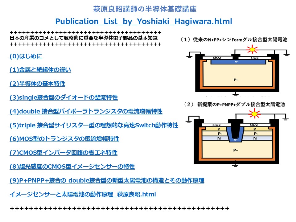
(0)はじめに
(1)金属と絶縁体の違い
(2)半導体の基本特性
(3)single接合型のダイオードの整流特性
(4)double 接合型バイポーラトランジスタの電流増幅特性
(5)triple 接合型サイリスター型の理想的な高速Switch動作特性
(6)MOS型のトランジスタの電流増幅特性
(7)CMOS型インバータ回路の省エネ特性
(8)超光感度のCMOS型イメージセンサーの特性
(9)P+PNPP+接合の double接合型の新型太陽電池の構造とその動作原理
イメージセンサーと太陽電池の動作原理_萩原良昭.html
超光感度半導体受光素子を太陽電池に使う事に挑戦します_萩原良昭.pdf
電子デバイス産業新聞2025年1月10日記事「ソニーの快男児、萩原良昭氏は新世代の鉄腕アトムを作る!」
2025_03_03_厚木市発SDGs支援団体_合同会社LOOMTEC社_AIPS萩原研究所の夢を実現に応援をお願いもうしあげます.pdf
電子デバイス産業新聞2025年1月10日記事「ソニーの快男児、萩原良昭氏は新世代の鉄腕アトムを作る!」
2025_03_03_厚木市発SDGs支援団体_合同会社LOOMTEC社_AIPS萩原研究所の夢を実現に応援をお願いもうしあげます.pdf
https://www.caltech.edu/ MS1971/BS1972/PhD1975
https://www.ieee.org/ IEEE Life Fellow
https://www.sojo-u.ac.jp/ 崇城大学特任教授
https://www.ssis.or.jp/ 半導体産業人協会会員
https://ja.wikipedia.org/wiki/萩原良昭
https://en.wikipedia.org/wiki/Yoshiaki_Hagiwara
Bio_and_List_of_Publications_Yoshiaki_Daimon_Hagiwara.pdf
Publication_List_by_Yoshiaki_Hagiwara.html
Hagiwara_履歴_2023_03_24.pdf
Bio_and_List_of_Publications_Yoshiaki_Daimon_Hagiwara.pdf
Publication_List_by_Yoshiaki_Hagiwara.html
HOP_応援募金活動報告_応援ありがとうございます_萩原良昭.html
Locomtec.jp/萩原aips研究所のご案内
Publication_List_by_Yoshiaki_Hagiwara.html
Introduction to the world of Super Light Sensitive Image Sensor and Solar Cell
The_Respectful_Words_of_Kawana_Yoshiyuki_on_Pinned_Photodiode.pdf Invention_an_Historical_Developmen_Efforts_of_Pinne_Burie_Photodiode.pdf Hagiwara_AIPS_Laboratory.html
Publication_List_by_Yoshiaki_Hagiwara.html
The_World_of_Digital_Circuits_for_AI_Robot_Applications_by_Yoshiaki_Daimon_Hagiwara_AIPS.pdf
The_World_of_Digital_Circuits_for_AI_Robot_Applications_by_Yoshiaki_Daimon_Hagiwara_AIPS_in_Japanese.html
The_World_of_Digital_Circuits_for_AI_Robot_Applications_by_Yoshiaki_Daimon_Hagiwara_AIPS_in_English.html
AIPS_251013.html AIPS_250912.html AIPS_250624.html AIPS_240822.html AIPS_240309.html AIPS_230316.html AIPS_221231.html AIPS_220823.html AIPS_220131.html AIPS_211226.html AIPS_211206.html AIPS_211107.html AIPS_210929.html AIPS_210906.html AIPS_210811.html AIPS_210404.html AIPS_210301.html AIPS_210217.html AIPS_210215.html AIPS_201209.html AIPS_200627.html AIPS_190925.html AIPS_190712.html AIPS_181129.html AIPS_090628.html 合同会社LOCOMTEC/萩原aips研究所
Publication_List_by_Yoshiaki_Hagiwara.html
https://www.sangyo-times.jp/article.aspx?ID=5331 Sangyo-Times.jp/article_ID=5331_(PDF) Sangyo-Times.jp/article_ID=5331_(html) Pinned_Buried_Photodiode_with_Electrical_Shutter_Function.pdf 2026_02_17_How_to_make_Multi_Junction_Solar_Cell_Yoshiaki_Hagiwara.pdf
How_to_make_Multi_Junction_Solar_Cell_Yoshiaki_Hagiwara.html
2026_02_19_ダブル接合型太陽電池の提案_萩原良昭.pdf
2026_02_12_How_to_make_Multi_Junction_Solar_Cell_Yoshiaki_Hagiwara_Top.pdf
2026_08_01_ICDIS2026.pdf
ICDIS2026
Dr. Yoshiaki Hagiwara is a key note speaker in ICDIS2026
2026_07_01_ICCCAS2026.pdf
ICCCAS2026
Dr. Yoshiaki Hagiwara is an invited speaker in ICCCAS2026
2025_05_23_ICCCAS2025_Yoshiaki_Daimon_Hagiwara_Wuhan_China_Slides.pdf
2025_05_23_ICCCAS2025_Yoshiaki_Daimon_Hagiwara_Wuhan_China_TEXT.pdf
2025_05_23_ICCCAS2025_Yoshiaki_Daimon_Hagiwara_Wuhan_China.mp4.
2025_05_12_ESP_Yoshiaki_Hagiwara_Double_Junction_Solar_Cell.pdf
Down_Load_2025_05_12_ESP_Yoshiaki_Hagiwara_Double_Junction_Solar_Cell.pdf
2024_05_10_ICCCAS2024_Slides_and_Presentation_mp4_Video_Files_by_Yoshiaki_Daimon_Hagiwara.pdf
ICCCAS2023_Conference_paper_on_"AIPS_with_Pinned_Buried_Photodiode_used_for_Robot_Vision_and_Solar_Cell_Panel"
P2023_IEEE_EDS_Newsletter_Jan_2023_on_Chronology_of_Silicon_based_Image_Sensor_Development.pdf
(P033) Dec 9 2021 ICECET2021 Paper75
P2021_ICECET2021_Paper75_on_Invention_and_Historical_Development_Efforts_of_Pinned_Burie_Photodiode.pdf
(P032) Dec 9 2021 ICECET2021 Paper61
P2021_ICECET2021_Paper61_on_Pinned_Buried_PIN_Photodiode_Type_Solar_Cell.pdf (P031) June 2021
http://www.sciencepublishinggroup.com/journal/paperinfo?journalid=245&doi=10.11648/j.ijssam.20210602.13 (P030) August 2020
(P029) March 2020
(P028) October 2019
(P027) April 2017
IEEE_CoolChips_2017_Conference_Invited_Panel_Talk_on_Intelligent_Image_Sensor_Systems.pdf (P026) June 2015
"Digital Frequency Transformation Circuit for Time-wise Unequally Sampled Data" (P025) July 2014
"Design of Time to Frequency Domain Discrete Fourier Transfer Hardware Engine and its performance estimation" (P024) July 2014
Japanese Patent Application JPA2014_135497 (P023) June 2013
"The p-n-p-n Diode in Future Linear Motor Cars and in Modern Imagers" (P022) February 2013
Invited Plenary Panel Talk at ISSCCC2013 on Feb. 2013 on Image Sensors (P021) May 2004
Artificial_Intelligent_Partner_System_AIPS_proposed_by_Yoshiaki_Hagiwara_on_May_2008.pdf
Sensor_Technology_in_World_Cup.pdf
Sony_Sensor_Technology_in_World_Cup.pdf
(P020) December 2004
Turorial Short Cource on Image Sesnors by Yoshiaki Hagiwara.pdf (P019) September 2001
"Micro-Electronics for Home Entertainment" (P018) November 1998
"DRAM/SRAM Technology and Problem.pdf" (P017) November 1997
"Sony Semiconductor History" (P016) December 1996
IEEE1996_Review_Paper_on_Sony_1980_One_Chip_FT_CCD_Image_Sensor (P015) October 1989
"A 25-ns 4-Mbit CMOS SRAM with Dynamic Bit-Line Loads" (P014) November 1980
Technology Book on "CCD Image Sensor and Applications" Trickeps Press, November 1980.(P013) May 1980
IEEE ECS1980 invited paper on "A CCD color imager with narrow-channel transfer gates" (P012) September 1979
"ADVANCES in CCD Imager " Technical Digest of IEEE International Conference (P011) September 1978
Hagiwara_SSDM1978_Paper_on_Pinned_Buried_Photodiode.pdf
P1978_SSDM1978_Paper_on_the_double_junction_type_Pinned_Photodiode.pdf (P010) September 1977
Japanese Patent Application JPA1977-126885 (P009) September 1977
P1977_Narrow_Cahnnel_Transfer_Gate_CCD_SSDM1977_Paper_by_Hagiwara.pdf" (P008) September 1976
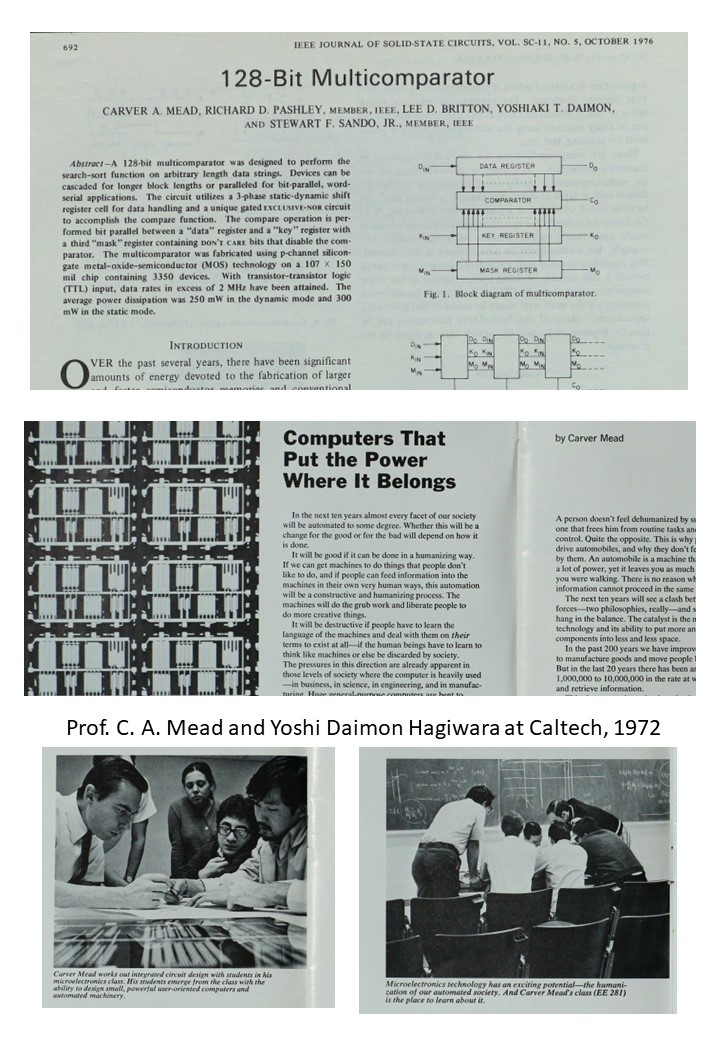
"128-Bit Multi Comparator" (P007) November 10 1975
Japanese Patent Application JPA1975-134985 (P006)October 23,1975
Japanese Patent Application JPA1975-127647 (P005) October 23,1975
Japanese Patent Application JPA1975-127646 (P004)June 1975
Caltech_1975_PhD_Thesis_by_Yoshiaki_Daimon_Hagihara.pdf (P003)April 1974
"Final Stage of the Charge Transfer Process in Charge Coupled Devices" (P002)February 1974
"Charge Transfer of Buried Channel Charge Coupled Devices" (P001)April 1973
"The Influence of Interface States on Incomplete Charge Transfer in Overlapping Gate Charge Coupled Devices"
Contributions to International Conferences and Organizations
++++++++++++++++++++++++++++++++++++++++++++++++++++http://icmts.if.t.u-tokyo.ac.jp/home http://isscc.org/ http://isscc.org/ https://www.coolchips.org/ https://www.coolchips.org/ https://www.caltech.edu/ https://www.gunma-u.ac.jp/ https://www.sojo-u.ac.jp/ http://www.aiplab.com// http://www.ssis.or.jp/ "Chronology_of_Silicon-based_Image_Sensor_development"- Y. D. Hagiwara.pdf
https://eds.ieee.org/images/files/newsletters/Newsletter_Jan23.pdf
IEEE_EDS_Newsletter_January2023_Issue.pdf
https://eds.ieee.org/publications/eds-newsletter
How_to_make_Multi_Junction_Solar_Cell_Yoshiaki_Hagiwara_91.pdf
小学生用半導体基礎講座_講師_萩原良昭.html
小学生用半導体基礎講座_1_10_2025_05_28.pdf
SONYのHADセンサー(Pinned_Photodiode)ダブル接合型太陽電池の提案.pdf
2025_02_13_LOCOMTEC_萩原AIPS研究所の活動紹介.pdf
2025_02_13_LOCOMTEC_萩原AIPS研究所の活動紹介.mp4
超光感度半導体受光素子を太陽電池に使う事に挑戦します_萩原良昭.pdf
C2025_02_23_シングルPN接合型太陽電池では空乏層幅は最大2μmが限界である事が簡単な計算で求まる_萩原良昭.pdf
C2025_02_22_シングルPN接合型太陽電池では空乏層幅は最大2μmが限界である事が簡単な計算で求まる_萩原良昭.pdf
C2025_01_20_Memo_Solar_Cell.pdf
Pinned_Surface_Completely_Depleted_Buried_Channel_Double_Junction_type_Solar_Cell.pdf
SONY(萩原良昭)のLife_Work_夢と挑戦.pdf
2025_02_11_良昭のひとりごと.mp4
C2025_01_23_Memo.pdf
Virtual_Gate_type_Solar_Cell_Process_by_Yoshiaki_Daimon_Hagiwara.pdf
Difference_between_Floating-Surface_and_Pinned_Surface_Photodiodes_by_Yoshiaki_Daimon_Hagiwara.pdf
Bio_and_List_of_Publications_Yoshiaki_Daimon_Hagiwara.pdf
Smart_AI_Robot_Vision_Image_Sensor_also_works_as_Solar_Cell_Yoshiaki_Hagiwara.pdf
Smart_AI_Robot_Vision_Image_Sensor_also_works_as_Solar_Cell_Yoshiaki_Hagiwara_01.mp4
Concept_of_Electron_Fog_amd_Solar_Cell_Band_Diagram.pdf
Electrostatic_Potential_Analysis_of_the_Pinned-surface_P+PNPsubP+_Double_Junction_Photodiode.pdf
2024_11_22_ICDIS2024_Conference_Slides_Link_Hagiwara.pdf
Locomtec.jp/萩原aips研究所のご案内
Hagiwara_履歴_2023_03_24.pdf
Publication_List_by_Yoshiaki_Hagiwara.html
Hagiwara_履歴_2023_03_24.pdf
2024_11_22_ICDIS2024_Key_Note_Yoshiaki_Daimon_Hagiwara_Sojo_University.pdf
2024_05_14_Reference_Papers_on_Pinned_Photodiode_type_Solar_Cell_by_Yoshiaki_Hagiwara.pdf
P2023_10_20_AIPE2023_Tokyo_Conference_Paper_on_AIPS_with_PBP_for_Robot_Vision_and_Solar_Cell_Panel.pdf
Hagiwara_履歴_2023_03_24.pdf
AIPS_Library_past_file_AIPS_090628_index.html
2024_05_10_ICCCAS2024_Slides_and_Presentation_mp4_Video_Files_by_Yoshiaki_Daimon_Hagiwara.pdf
http://www.icccas.org/
ICCCAS2023_Conference_paper_on_"AIPS_with_Pinned_Buried_Photodiode_used_for_Robot_Vision_and_Solar_Cell_Panel"
"Chronology_of_Silicon-based_Image_Sensor_development"- Y. D. Hagiwara.pdf
https://eds.ieee.org/images/files/newsletters/Newsletter_Jan23.pdf
IEEE_EDS_Newsletter_January2023_Issue.pdf
https://eds.ieee.org/publications/eds-newsletter
2024_04_Publication_List_and_Bio_Yoshiaki_Daimon_Hagiwara.pdf
http://www.aiplab.com/
Evidence_that_Hagiwara_at_Sony_invented_Pinned_Buried_Photodiode_in_1975.pdf
http://www.aiplab.com/
Yoshiaki_Hagiwara_Bio.pdf
Virtual_Phase_Clock_Operation_Scheme_became_possible
Virtual_Phase_Clock_Operation_Scheme_became_possible
slides_pdf.file
P2019_3DIC2019_Paper_on_3D_Pinned_Photodiode_6_pages.pdf
P2020_EDTM2020_PaperID_3C4_by_Hagiwara_4_pages.pdf
EDTM2020_Paper_on_the P+PN+P Junction Pinned Photodiode and Schottky Barrier Photodiode.html
P2021_IJSSA2021_Paper_20210616_on_Electrostatic_and_Dynamic_Analysis_of_Pinned_Photodiodes.pdf
P2021_IJSSA2021_Paper_20210616_on_Electrostatic_and_Dynamic_Analysis_of_Pinned_Photodiodes.html
ICECET2021_Paper61_html
ICECET2021_Paper75_html
Chronology_of_Silicon_based_Image_Sensor_Development
http://www.icecet.com/home http://www.icecet.com/ICECET_Program.pdf ICECET2021_Session_E-III_chaired_by_Yoshiaki_Hagiwara.pdf ICECET2021_Program_Session_E-III.pdf ICECET2021_Paper61_html ICECET2021_Paper75_html http://www.icecet.com/home http://www.icecet.com/ICECET_Program.pdf ICECET2021_Session_E-III_chaired_by_Yoshiaki_Hagiwara.pdf 001A_ICECET2021_Paper061_Pinned Buried PIN Photodiode type Solar Cell.pdf 001B_ICECET2021_acceptance_letter_ID_061.pdf 001C_ICECET 2021_PARTICIPATION_CERTIFICATE_061.pdf 001D_ICECET2021_Paper061_supplement_Process_Flow_of_Pinned_Buried_PIN_Photodiode_type_Solar_Cell_2021_08_14.pdf 002A_ICECET2021_Paper075_Invention and Historical Development Efforts of Pinned Buried Photodiode.pdf 002B_ICECET2021_acceptance_letter_ID_075.pdf 002C_ICECET 2021 PARTICIPATION CERTIFICATE_075.pdf 002D_ICECET2021_Paper075_supplement_The_Evidence_that_Hagiwar_at_Sony_invente_Pinne_Burie_Photodiode_in_1975.pdf 003_ICECET2021_CHAIR_CERTIFICATE_Session_E3.pdf 004_ICECET2001_Session_E-III_Chaired_by_Yoshiaki_Hagiwara.pdf Sony_vs_Loral_Patent_War_1_Reviews.pdf Sony_vs_Loral_Patent_War_2_Supporting_Opinions.pdf E-mail_Communication_on_Sony_Loral_Patent_War_1996.pdf E-mail_communication_with_Albert_san_2018_07_10.pdf HAD_sensor_NEC_SONY_Patent_War.pdf JP1980_138026_NEC_Buried_Photodiode_Patent.pdf JP1978-1971_Toshiba_Yamada_VOD_patent.pdf Sony_vs_Loral_PAtent_War_13_pages.pdf Sony_vs_Loral_Patent_War_53_pages.pdf Image_Sensor_Story_by_Hagiwara.pdf The_evidence_that_Hagiwara_is_the_inventor_of_Pinned_Photodiode_7_pages.pdf Future_of_Image_Sensors_and_Solar_Cells.pdf JP1975-127646_NPNP_triple_junction_Pinned_Photodiode_Patent_32_pages.pdf The_First_Pinned_Photodiode_was_invented_in_1975_by_Yoshiaki_Hagiwar_at_Sony.pdf JP1975-127647_NPN_double_junction_Pinned_Photodiode_Patent_22_pages.pdf JP1975-134985_PNP_double_junction_Pinned_Photodiode_on_Nsub_Patent_7_pages.pdf JP1977-126885_Elecric_Shutter_Clocking_Scheme_by_OFD_Punch_Thru_Action_13_pages.pdf JP2014-135497_Digital_Transformation_Circuit_for_Image_Sensors_29_pages.pdf JP2020_131313_on_Doubel_Junction_Pinned_Photodiode_Solar_Cell_65_Pages.pdf JPA_2020_131313_Japan_Patent_6818208_on_Pinned_Photodiode_type_Solar_Cell_by_Hagiwara.pdf P1978_Pinned_Photodiode_1978_Paper_by_Hagiwara_7_Pages.pdf P1996_Pinned_Photodidoe_used_in_Sony_1980_FT_CCD_Image_Sensor_9_Pages.pdf P2001_ESSCIRC2001_Micro-Electronics_for_Home_Entertainment_11_pages.pdf P2008_ESSCIRC_2008_SOI_Design_in_Cell_Processor_and_Beyond_7_pages.pdf P2013_ISSCC2013_Panel_Talk_25_pages.pdf P2017_CoolChips_Panel_170419_29_pages.pdf P2019_3DIC2019_Paper_on_3D_Pinned_Photodiode_6_pages.pdf P2020_EDTM2020_PaperID_3C4_by_Hagiwara_4_pages.pdf P2021_IJSSA2021_Paper_20210616_on_Electrostatic_and_Dynamic_Analysis_of_Pinned_Photodiodes.pdf ICECET2021_Paper61_html ICECET2021_Paper75_html Chronology_of_Silicon_based_Image_Sensor_Development
Buried_Photodiode_is_not_always_PPD_Hagiwara_Nov_2020.pdf Caltech_1975_PhD_Thesis_Yoshiaki_Daimon_Hagihara.pdf Difference_of_Buried_Photodiode_and_Pinned_Photodiode.pdf E-mail_Communication_on_Sony_Loral_Patent_War_1996.pdf E-mail_communication_with_Albert_and_Yoshi.pdf E-mail_communication_with_Albert_san_2018_07_10.pdf E-mail_communication_with_Albert_san_2018_07_10A.pdf E-mail_communication_with_Albert_san_2018_07_10B.pdf Evidence_that_Hagiwara_is_the_inventor_of_Pinned_Photodiode_2020_10_04a.pdf Evidence_that_Hagiwara_is_the_inventor_of_Pinned_Photodiode_in_Japanese.pdf https://www.seizansha.co.jp/ISBN/ISBN978-4-88359-339-2.html https://www.seizansha.co.jp/ https://www.sangyo-times.jp/article.aspx?ID=5331 Sangyo-Times.jp/article_ID=5331_(PDF) Sangyo-Times.jp/article_ID=5331_(html) Candy_in_the_Heart TOP 010 ,
020 ,
030 ,
040 ,
050 ,
060 ,
070 ,
080 ,
090 ,
100 110 ,
120 ,
130 ,
140 ,
150 ,
160 ,
170 ,
180 ,
190 ,
200 210 ,
220 ,
230 ,
240 ,
250 ,
260 ,
270 ,
280 ,
290 ,
300 310 ,
320 ,
330 ,
340 ,
350 ,
360 ,
370 ,
380 ,
390 ,
400 410 ,
420 ,
430 ,
440 ,
450 ,
460 ,
470 ,
480 ,
490 ,
500 510 ,
520 ,
530 ,
540 ,
550 ,
560 ,
570 ,
580 ,
590 ,
600 610 ,
620
2022_06_07_Gunma_Top.html
人工知能ロボットを支える、超光感度の賢い電子の目を太陽電池に応用する
Please_Support_Our_Activity.html
新型太陽電池の開発推進活動をご支援していただける有志を募集案内です
(0)はじめに
(1)金属と絶縁体の違い
(2)半導体の基本特性
(3)single接合型のダイオードの整流特性
(4)double 接合型バイポーラトランジスタの電流増幅特性
(5)triple 接合型サイリスター型の理想的な高速Switch動作特性
(6)MOS型のトランジスタの電流増幅特性
(7)CMOS型インバータ回路の省エネ特性
(8)超光感度のCMOS型イメージセンサーの特性
(9)P+PNPP+接合の double接合型の新型太陽電池の構造とその動作原理
イメージセンサーと太陽電池の動作原理_萩原良昭.html
超光感度半導体受光素子を太陽電池に使う事に挑戦します_萩原良昭.pdf
電子デバイス産業新聞2025年1月10日記事「ソニーの快男児、萩原良昭氏は新世代の鉄腕アトムを作る!」
2025_03_03_厚木市発SDGs支援団体_合同会社LOOMTEC社_AIPS萩原研究所の夢を実現に応援をお願いもうしあげます.pdf
電子デバイス産業新聞2025年1月10日記事「ソニーの快男児、萩原良昭氏は新世代の鉄腕アトムを作る!」
2025_03_03_厚木市発SDGs支援団体_合同会社LOOMTEC社_AIPS萩原研究所の夢を実現に応援をお願いもうしあげます.pdf
https://www.caltech.edu/ MS1971/BS1972/PhD1975
https://www.ieee.org/ IEEE Life Fellow
https://www.sojo-u.ac.jp/ 崇城大学特任教授
https://www.ssis.or.jp/ 半導体産業人協会会員
https://ja.wikipedia.org/wiki/萩原良昭
https://en.wikipedia.org/wiki/Yoshiaki_Hagiwara
Bio_and_List_of_Publications_Yoshiaki_Daimon_Hagiwara.pdf
Publication_List_by_Yoshiaki_Hagiwara.html
Hagiwara_履歴_2023_03_24.pdf
Bio_and_List_of_Publications_Yoshiaki_Daimon_Hagiwara.pdf
Publication_List_by_Yoshiaki_Hagiwara.html
HOP_応援募金活動報告_応援ありがとうございます_萩原良昭.html
Locomtec.jp/萩原aips研究所のご案内
Publication_List_by_Yoshiaki_Hagiwara.html
Introduction to the world of Super Light Sensitive Image Sensor and Solar Cell
The_Respectful_Words_of_Kawana_Yoshiyuki_on_Pinned_Photodiode.pdf Invention_an_Historical_Developmen_Efforts_of_Pinne_Burie_Photodiode.pdf Hagiwara_AIPS_Laboratory.html
Publication_List_by_Yoshiaki_Hagiwara.html
The_World_of_Digital_Circuits_for_AI_Robot_Applications_by_Yoshiaki_Daimon_Hagiwara_AIPS.pdf
The_World_of_Digital_Circuits_for_AI_Robot_Applications_by_Yoshiaki_Daimon_Hagiwara_AIPS_in_Japanese.html
The_World_of_Digital_Circuits_for_AI_Robot_Applications_by_Yoshiaki_Daimon_Hagiwara_AIPS_in_English.html
AIPS_251013.html AIPS_250912.html AIPS_250624.html AIPS_240822.html AIPS_240309.html AIPS_230316.html AIPS_221231.html AIPS_220823.html AIPS_220131.html AIPS_211226.html AIPS_211206.html AIPS_211107.html AIPS_210929.html AIPS_210906.html AIPS_210811.html AIPS_210404.html AIPS_210301.html AIPS_210217.html AIPS_210215.html AIPS_201209.html AIPS_200627.html AIPS_190925.html AIPS_190712.html AIPS_181129.html AIPS_090628.html TOP_Page 001 ,
002 ,
003 ,
004 ,
005 ,
006 ,
007 ,
008 ,
009 ,
010 011 ,
012 ,
013 ,
014 ,
015 ,
016 ,
017 ,
018 ,
019 ,
020 021 ,
022 ,
023 ,
024 ,
025 ,
026 ,
027 ,
028 ,
029 ,
030 031 ,
032 ,
033 ,
034 ,
035 ,
036 ,
037 ,
038 ,
039 ,
040 041 ,
042 ,
043 ,
044 ,
045 Hagiwara_AIPS_Laboratory.html
Jump to Top

.jpg)


設立の提案_LOCOMTEC社萩原aips研究所.jpg)
搭載のロボット.jpg)

ダブル接合型太陽電池の提案_LOCOMTEC_萩原研究所_萩原良昭.jpg)


のLife_Work_夢と挑戦_1.jpg)


のLife_Work_夢と挑戦_2.jpg)
のLife_Work_夢と挑戦_3.jpg)