++++++++++++++++++++++++++++++++++++++++++++++++++++++
Hagiwara AIPS Library Page 43
++++++++++++++++++++++++++++++++++++++++++++++++++++++
++++++++++++++++++++++++++++++++++++++++++++++++++++++
Recent Publications on Pinned Photodiode
++++++++++++++++++++++++++++++++++++
(R26) P2019_3DIC2019_Paper_on_3D_Pinned_Photodiode_6_pages.pdf
(R27) P2020_EDTM2020_PaperID_3C4_by_Hagiwara_4_pages.pdf
EDTM2020_Paper_on_the P+PN+P Junction Pinned Photodiode and Schottky Barrier Photodiode.html
(R28) P2021_IJSSA2021_Paper_20210616_on_Electrostatic_and_Dynamic_Analysis_of_Pinned_Photodiodes.pdf
P2021_IJSSA2021_Paper_20210616_on_Electrostatic_and_Dynamic_Analysis_of_Pinned_Photodiodes.html
(R29) ICECET2021_Paper61_html
(R30) ICECET2021_Paper75_html
(R31) Chronology_of_Silicon_based_Image_Sensor_Development
IEEE_Electron_Devices_Society_Newsletter_January_2023
++++++++++++++++++++++++++++++++++++
http://www.icecet.com/home
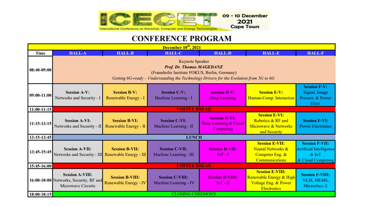
http://www.icecet.com/ICECET_Program.pdf
ICECET2021_Session_E-III_chaired_by_Yoshiaki_Hagiwara.pdf
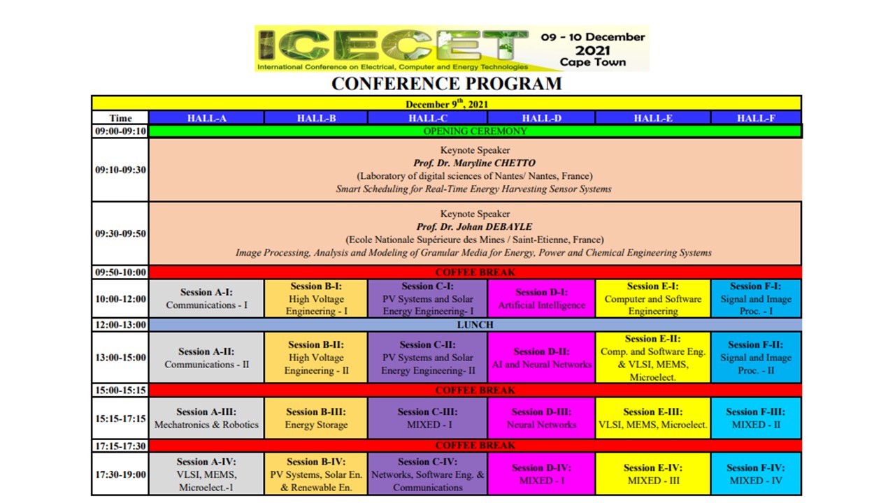
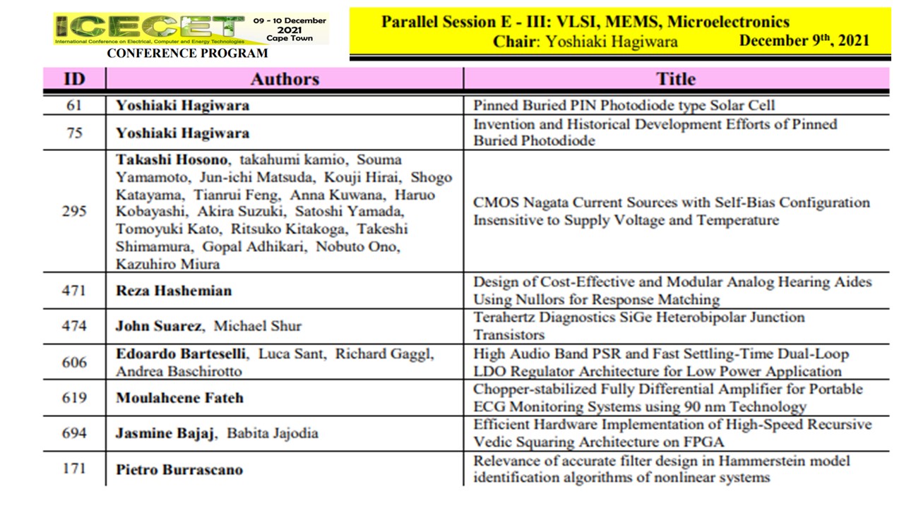
ICECET2021_Program_Session_E-III.pdf
++++++++++++++++++++++++++++++++++++
The presentation slides, pdf, mp3 audio and mp4 video files
of my papers 061 and 075 are now all uploaded into:
(R29) ICECET2021_Paper61_html
(R30) ICECET2021_Paper75_html
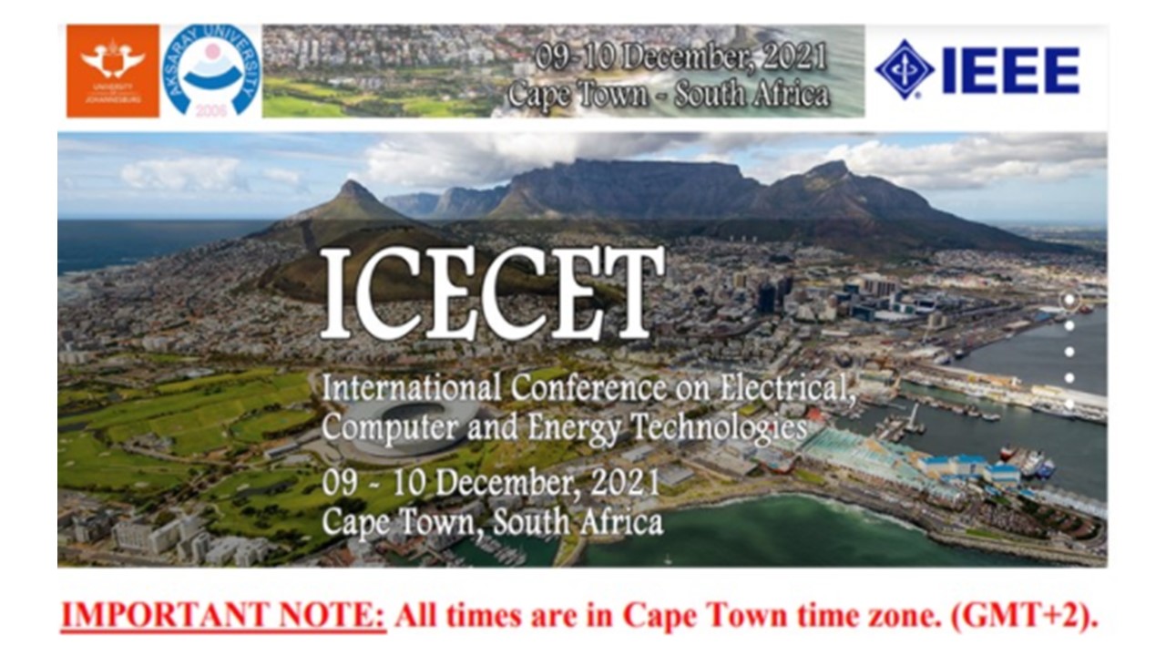
held at the IEEE ICECET2021 conference
in Cape Town, South Afrrica on Dec 9 and 10, 2021.
http://www.icecet.com/home
http://www.icecet.com/ICECET_Program.pdf
ICECET2021_Session_E-III_chaired_by_Yoshiaki_Hagiwara.pdf
*************************************************************
001A_ICECET2021_Paper061_Pinned Buried PIN Photodiode type Solar Cell.pdf
001B_ICECET2021_acceptance_letter_ID_061.pdf
001C_ICECET 2021_PARTICIPATION_CERTIFICATE_061.pdf
001D_ICECET2021_Paper061_supplement_Process_Flow_of_Pinned_Buried_PIN_Photodiode_type_Solar_Cell_2021_08_14.pdf
002A_ICECET2021_Paper075_Invention and Historical Development Efforts of Pinned Buried Photodiode.pdf
002B_ICECET2021_acceptance_letter_ID_075.pdf
002C_ICECET 2021 PARTICIPATION CERTIFICATE_075.pdf
002D_ICECET2021_Paper075_supplement_The_Evidence_that_Hagiwar_at_Sony_invente_Pinne_Burie_Photodiode_in_1975.pdf
003_ICECET2021_CHAIR_CERTIFICATE_Session_E3.pdf
004_ICECET2001_Session_E-III_Chaired_by_Yoshiaki_Hagiwara.pdf
*************************************************************
+++++++++++++++++++++++++++++++++++++++++++++++++++++++++++++++
List of Realted PDF files decribing the works of Yoshiaki Hagiwara
+++++++++++++++++++++++++++++++++++++++++++++++++++++++++++++++
(R01) Sony_vs_Loral_Patent_War_1_Reviews.pdf
(R02) Sony_vs_Loral_Patent_War_2_Supporting_Opinions.pdf
(R03) E-mail_Communication_on_Sony_Loral_Patent_War_1996.pdf
(R04) E-mail_communication_with_Albert_san_2018_07_10.pdf
(R05) HAD_sensor_NEC_SONY_Patent_War.pdf
(R06) JP1980_138026_NEC_Buried_Photodiode_Patent.pdf
(R07) JP1978-1971_Toshiba_Yamada_VOD_patent.pdf
(R08) Sony_vs_Loral_PAtent_War_13_pages.pdf
(R09) Sony_vs_Loral_Patent_War_53_pages.pdf
(R10) Image_Sensor_Story_by_Hagiwara.pdf
(R11) The_evidence_that_Hagiwara_is_the_inventor_of_Pinned_Photodiode_7_pages.pdf
(R12) Future_of_Image_Sensors_and_Solar_Cells.pdf
(R13) JP1975-127646_NPNP_triple_junction_Pinned_Photodiode_Patent_32_pages.pdf
(R14) The_First_Pinned_Photodiode_was_invented_in_1975_by_Yoshiaki_Hagiwar_at_Sony.pdf
(R15) JP1975-127647_NPN_double_junction_Pinned_Photodiode_Patent_22_pages.pdf
(R16) JP1975-134985_PNP_double_junction_Pinned_Photodiode_on_Nsub_Patent_7_pages.pdf
(R17) JP1977-126885_Elecric_Shutter_Clocking_Scheme_by_OFD_Punch_Thru_Action_13_pages.pdf
(R18) JP2014-135497_Digital_Transformation_Circuit_for_Image_Sensors_29_pages.pdf
(R19) JP2020_131313_on_Doubel_Junction_Pinned_Photodiode_Solar_Cell_65_Pages.pdf
(R19A) JPA_2020_131313_Japan_Patent_6818208_on_Pinned_Photodiode_type_Solar_Cell_by_Hagiwara.pdf
(R20) P1978_Pinned_Photodiode_1978_Paper_by_Hagiwara_7_Pages.pdf
(R21) P1996_Pinned_Photodidoe_used_in_Sony_1980_FT_CCD_Image_Sensor_9_Pages.pdf
(R22) P2001_ESSCIRC2001_Micro-Electronics_for_Home_Entertainment_11_pages.pdf
(R23) P2008_ESSCIRC_2008_SOI_Design_in_Cell_Processor_and_Beyond_7_pages.pdf
(R24) P2013_ISSCC2013_Panel_Talk_25_pages.pdf
(R25) P2017_CoolChips_Panel_170419_29_pages.pdf
(R26) P2019_3DIC2019_Paper_on_3D_Pinned_Photodiode_6_pages.pdf
(R27) P2020_EDTM2020_PaperID_3C4_by_Hagiwara_4_pages.pdf
(R28) P2021_IJSSA2021_Paper_20210616_on_Electrostatic_and_Dynamic_Analysis_of_Pinned_Photodiodes.pdf
(R29) ICECET2021_Paper61_html
(R30) ICECET2021_Paper75_html
(R31) Chronology_of_Silicon_based_Image_Sensor_Development
IEEE_Electron_Devices_Society_Newsletter_January_2023
++++++++++++++++++++++++++++++++++++++++++++++++++++++++++++++++++++++
(Q01) Buried_Photodiode_is_not_always_PPD_Hagiwara_Nov_2020.pdf
(Q02) Caltech_1975_PhD_Thesis_Yoshiaki_Daimon_Hagihara.pdf
(Q03) Difference_of_Buried_Photodiode_and_Pinned_Photodiode.pdf
(Q04) E-mail_Communication_on_Sony_Loral_Patent_War_1996.pdf
(Q05) E-mail_communication_with_Albert_and_Yoshi.pdf
(Q06) E-mail_communication_with_Albert_san_2018_07_10.pdf
(Q07) E-mail_communication_with_Albert_san_2018_07_10A.pdf
(Q08) E-mail_communication_with_Albert_san_2018_07_10B.pdf
(Q09) Evidence_that_Hagiwara_is_the_inventor_of_Pinned_Photodiode_2020_10_04a.pdf
(Q10) Evidence_that_Hagiwara_is_the_inventor_of_Pinned_Photodiode_in_Japanese.pdf
+++++++++++++++++++++++++++++++++++++++++++++++++++++++++
+++++++++++++++++++++++++++++++++++++++++++++++++++++++++
Introduction to the world of Digital Circuits for Artificial Intelligence
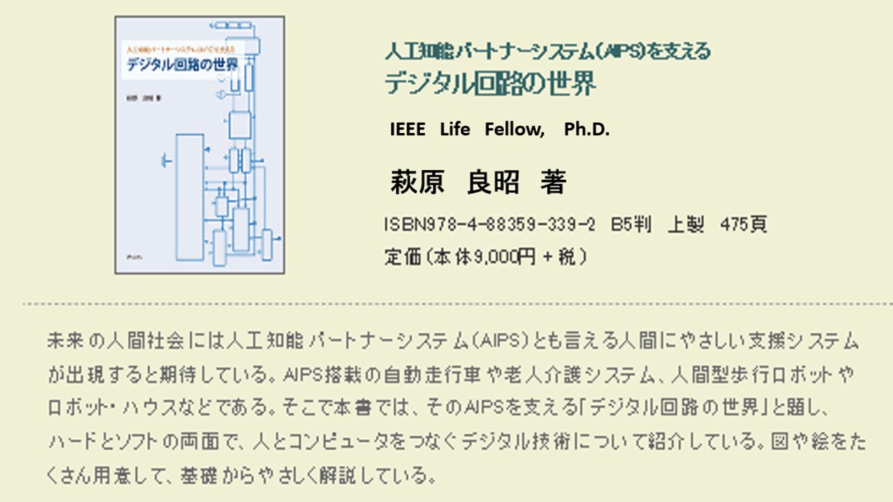
If you are interestied in the book, Please visit
https://www.seizansha.co.jp/ISBN/ISBN978-4-88359-339-2.html
https://www.seizansha.co.jp/
++++++++++++++++++++++++++++++++++++++++++++++++++++++
Jump to Page 44
+++++++++++++++++++++++++++++++++++++++++++++++++++++++++
Hagiwara_AIPS_Laboratory.html
++++++++++++++++++++++++++++++++++++++++++++
Jump to Page
TOP_Page
001,
002,
003,
004,
005,
006,
007,
008,
009,
010
011,
012,
013,
014,
015,
016,
017,
018,
019,
020
021,
022,
023,
024,
025,
026,
027,
028,
029,
030
031,
032,
033,
034,
035,
036,
037,
038,
039,
040
041,
042,
043,
044,
045
+++++++++++++++++++++++++++++++++++++++++++