++++++++++++++++++++++++++++++++++++++++++++++++++++++
Hagiwara AIPS Library Page 40
++++++++++++++++++++++++++++++++++++++++++++++++++++++
++++++++++++++++++++++++++++++++
(P021) May 2004
++++++++++++++++++++++++++++++++++++++++++++++++++
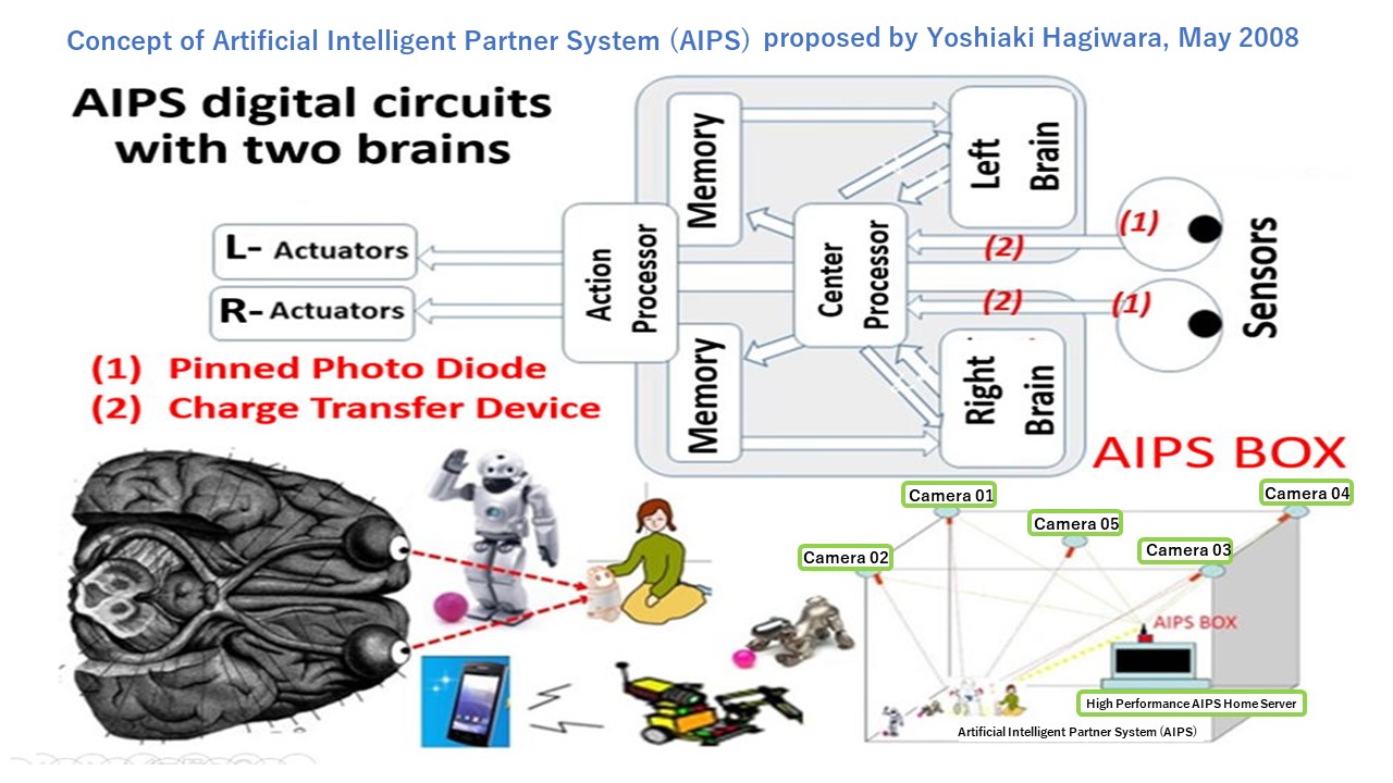
Artificial_Intelligent_Partner_System_AIPS_proposed_by_Yoshiaki_Hagiwara_on_May_2008.pdf
++++++++++++++++++++++++++++++++++++++++++++++++++++++
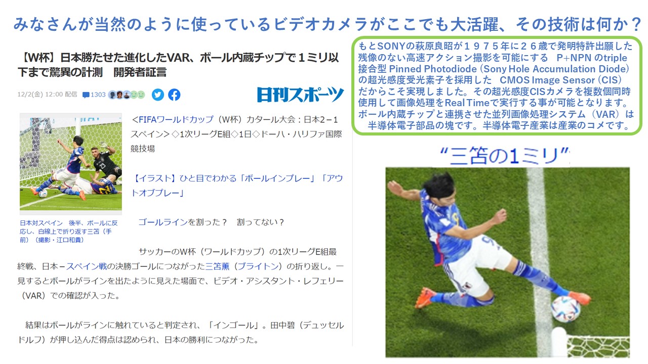
Sensor_Technology_in_World_Cup.pdf
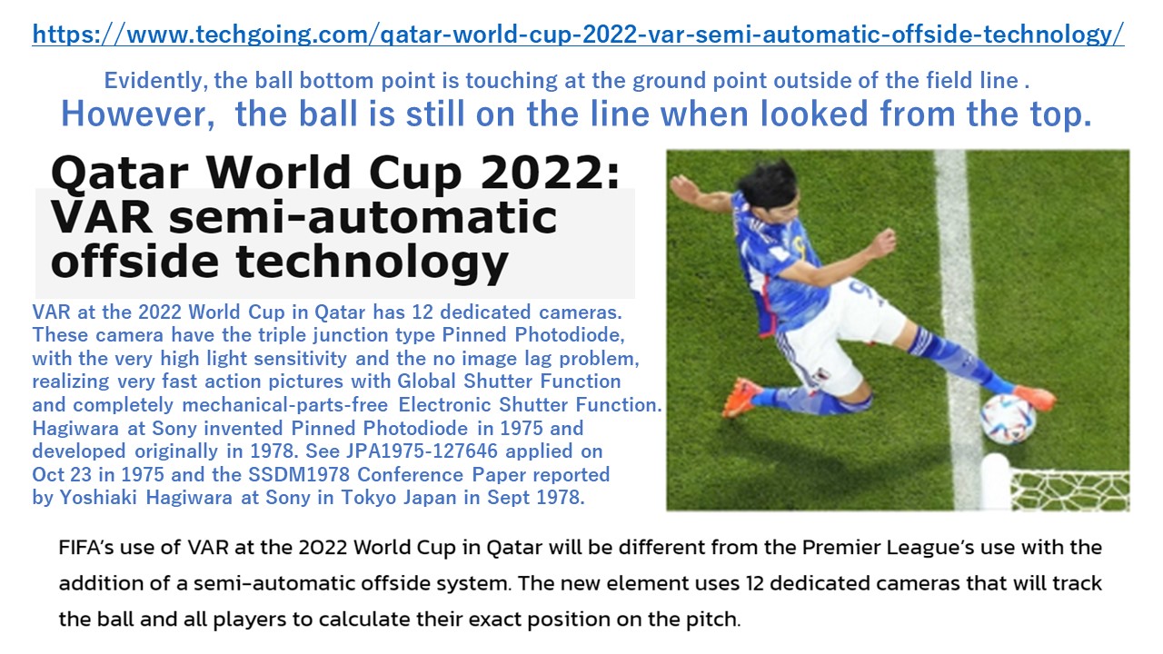
Sony_Sensor_Technology_in_World_Cup.pdf
++++++++++++++++++++++++++++++++++++++++++++++++++++++
(P021A) September 2008
"SOI Design in Cell Processor and Beyond"
an invited ESSCIRC2008 Plenary Talk, Technical Digest of IEEE ESSCIRC2008 Conference,
Edinburgh, Scotland UK, September 2008.
(P021B) December 2008
"Prospect of Developing AIPS Robots for Home Total Supporting Systems"
IEICE technical report, December 12, 2008,ICD2008 Conference, Tokyo, Japan,Vol 108-247, pp.85-90
++++++++++++++++++++++++++++++++++++++++++++++++++++++
(P020) December 2004
Turorial Short Cource on Image Sesnors by Yoshiaki Hagiwara.pdf
IEEE IEDM2004 Conference Short Course at IEDM2004 Short Course, December 2004.
(P019) September 2001
"Micro-Electronics for Home Entertainment"
an invited ESSCIRC2001 Plenary Talk,
Technical Digest of IEEE ESSCIRC2001 International Conference (ESSCIRC2001),
Villach, Austria, September, 2001.
(P018) November 1998
"DRAM/SRAM Technology and Problem.pdf"
Proceedings of the Institute of Electrostatics Japan,
127 Vol. 22 No. 6, 1998, pp.177-178.
(P017) November 1997
"Sony Semiconductor History"
Addressed at the 23th Research Seminar
in Tokyo Communication University, Nov 28, 1997.
(P016) December 1996
IEEE1996_Review_Paper_on_Sony_1980_One_Chip_FT_CCD_Image_Sensor
with_Pinned_Buried_Photodiode
IEEE Transaction on electron Devices, VOl.43, No.12, Dec 1996.
(P015) October 1989
"A 25-ns 4-Mbit CMOS SRAM with Dynamic Bit-Line Loads"
IEEE Journal of Solid State Circuits, vol.24, no.5, October 1989.
(P014) November 1980
Technology Book on "CCD Image Sensor and Applications" Trickeps Press, November 1980.
(P013) May 1980
IEEE ECS1980 invited paper on "A CCD color imager with narrow-channel transfer gates"
Proceeding of the 157th Electrochemical Society Meeting, May 11-16, 1980, St. Luis, USA.
(P012) September 1979
"ADVANCES in CCD Imager " Technical Digest of IEEE International Conference
of CCD Image Sensors (IEEE CCD'79),Edinburgh, Scotland UK, September 1979.
(P011) September 1978
Hagiwara_SSDM1978_Paper_on_Pinned_Buried_Photodiode.pdf
Proceeding of the 10th Conference on Solid State Devices,Tokyo, September 1978.
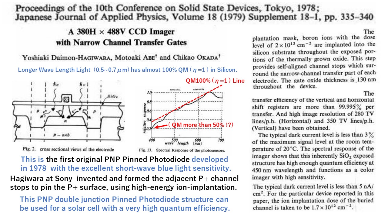
P1978_SSDM1978_Paper_on_the_double_junction_type_Pinned_Photodiode.pdf
(P010) September 1977
Japanese Patent Application JPA1977-126885
on "Electric Shutter Clocking and Gamma Control Scheme
using Overflow Drain (OFD) controlled by Strong Punch Thru OFD Voltage Control",
Japanese Patent Application written in Japanese,filed on Sep 29, 1977
(P009) September 1977
P1977_Narrow_Cahnnel_Transfer_Gate_CCD_SSDM1977_Paper_by_Hagiwara.pdf"
Proceeding of the 9th Conference on Solid State Devices,Tokyo, September 1977
(P008) September 1976
"128-Bit Multi Comparator"
IEEE Journal of Solid State Circuits, VOL.SC11, No.4, October 1976.
(P007) November 10 1975
Japanese Patent Application JPA1975-134985
on "Triple Junction Type Pinned Buried Photodiode
with Complete Charge Transfer Capability and
Vertical Overflow Drain Function",Japanese Patent Application
written in Japanese, filed on Nov 10, 1975.
(P006)October 23,1975
Japanese Patent Application JPA1975-127647
on "Back-light Double Junction Type Pinned Buried Photodiode
with Complete Charge Transfer Capability and Global Shutter Function",
Japanese Patent Application written in Japanese, filed on Oct 23, 1975
(P005) October 23,1975
Japanese Patent Application JPA1975-127646
on "Back-light Triple Junction Type Pinned Buried Photodiode
with Complete Charge Transfer Capability and Global Shutter Fucntion",
Japanese PAtent Application written in Japanese, filed on Oct 23, 1975
(P004)June 1975
Caltech_1975_PhD_Thesis_by_Yoshiaki_Daimon_Hagihara.pdf
in Electrical Engineering (major) and Physics(minor), June 1975,
California Institute of Technology, Pasadena, California USA.
(P003)April 1974
"Final Stage of the Charge Transfer Process in Charge Coupled Devices"
IEEE Transactions on Electron Devices, Vol. ED-21, No.4, April 1974
(P002)February 1974
"Charge Transfer of Buried Channel Charge Coupled Devices"
Proceeding of International Solid State Circuit Conference
(ISSCC1974),San Francisco, February 1974.
(P001)April 1973
"The Influence of Interface States on Incomplete Charge Transfer in Overlapping Gate Charge Coupled Devices"
IEEE Journal of Solid State Circuits,Vol. SC 8, No.2, April 1973
+++++++++++++++++++++++++++++++++++++++++++++++++++++++++++++++++++++++++++++++++++++++++++++++++++++++++++++++++++++++
++++++++++++++++++++++++++++++++++++++++++++++++++++
Contributions to International Conferences and Organizations
++++++++++++++++++++++++++++++++++++++++++++++++++++
(C01) International Standardization Committee (1989-1992)
IEC TC47 Technical Committee Chair (1992)
(C02) JEDEC Memory Chips Standardization Committee (2000-2004)
(C03) IEEE EDS ICMTS International Program and Executive Committee (1991-2008)
General Chair (2003-2004);http://icmts.if.t.u-tokyo.ac.jp/home
(C04) IEEE SSS ISSCC Asian Program Committee (2001-2007)
ISSCC Asian Chair (2006-2007);http://isscc.org/
(C05) IEEE SSS ISSCC2008 International Program and Executive Committee (2007-2008)
International Program Chair (2007-2008); http://isscc.org/
(C06) IEEE Computer Society Cool Chips Organization Committee (2001-2010)
https://www.coolchips.org/
(C07) IEEE Computer Society Cool Chips Advisory Committee (2011-2021)
https://www.coolchips.org/
(C08) Visiting Professorship in Electric Engineering Department and
Applied Physics Department at California Institute of Technology,
Pasadena, califor, USA, 1998-1999;https://www.caltech.edu/
(C09) Professorship in Electircal Engineering Department at Gunma University,
Kiryu-city, Gunma-ken, Japan, 2001-2008;https://www.gunma-u.ac.jp/
(C10) Professorship in Information and Communication Tecnology Department
at Sojo University, Kumamoto-city, Japan, 2009-2017; https://www.sojo-u.ac.jp/
(C11) Artificial Intelligent Partner System (AIPS) Consortium,Kanagawa-ken NPO, Japan,
President and CEO (2008-2017); http://www.aiplab.com//
(C12) Society of Semiconductore Industry Experts of Japan ; http://www.ssis.or.jp/
currently also serving as the chairman of the SSIS Education Executive Committee.
++++++++++++++++++++++++++++++++++++++++++++++++++++++++++++++++++++++++++
++++++++++++++++++++++++++++++++++++++++++++++++++++++
Jump to Page 41
+++++++++++++++++++++++++++++++++++++++++++++++++++++++++
Hagiwara_AIPS_Laboratory.html
++++++++++++++++++++++++++++++++++++++++++++
Jump to Page
TOP_Page
001,
002,
003,
004,
005,
006,
007,
008,
009,
010
011,
012,
013,
014,
015,
016,
017,
018,
019,
020
021,
022,
023,
024,
025,
026,
027,
028,
029,
030
031,
032,
033,
034,
035,
036,
037,
038,
039,
040
041,
042,
043,
044,
045
+++++++++++++++++++++++++++++++++++++++++++