++++++++++++++++++++++++++++++++++++++++++++++++++++++
Hagiwara AIPS Library Page 24
++++++++++++++++++++++++++++++++++++++++++++++++++++++
++++++++++++++++++++++++++++++++++++++++++++++++++++++++++++++++++++++++++
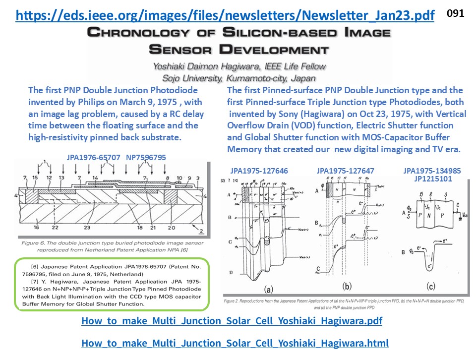
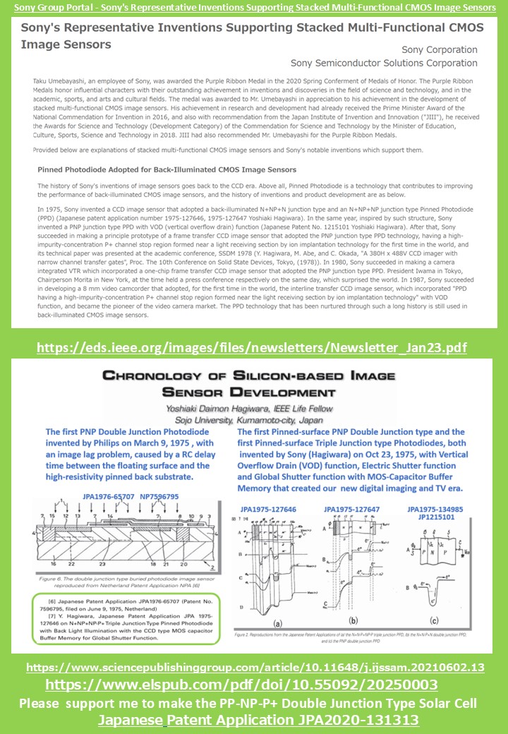
"Chronology_of_Silicon-based_Image_Sensor_development"- Y. D. Hagiwara.pdf
https://eds.ieee.org/images/files/newsletters/Newsletter_Jan23.pdf
is on
IEEE_EDS_Newsletter_January2023_Issue.pdf
https://eds.ieee.org/publications/eds-newsletter
++++++++++++++++++++++++++++++++++++++++++++++++++++++
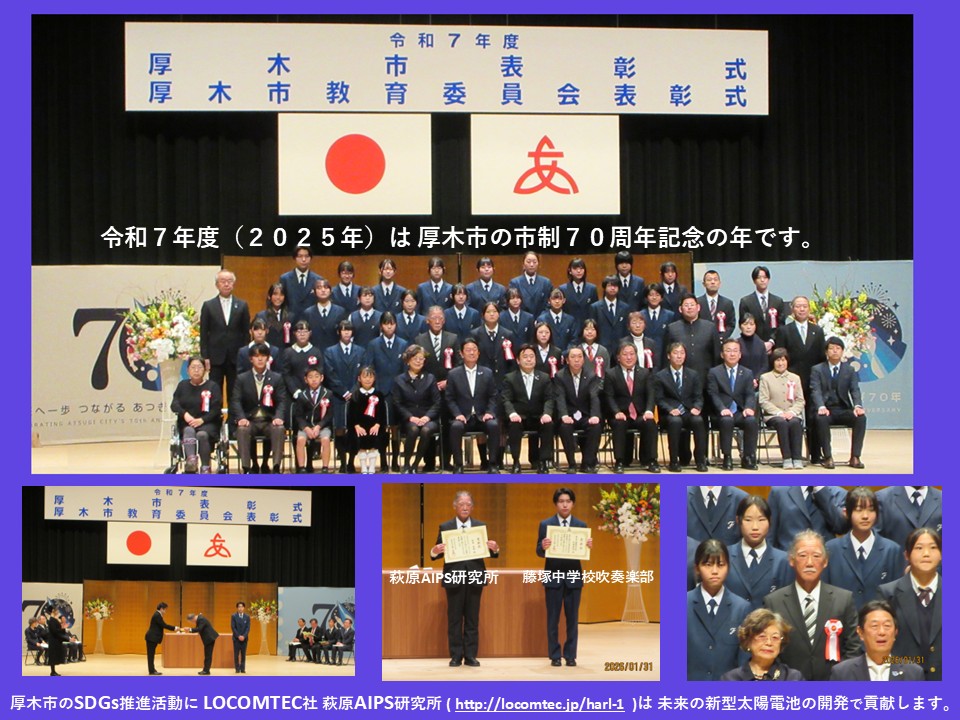
How_to_make_Multi_Junction_Solar_Cell_Yoshiaki_Hagiwara_91.pdf
++++++++++++++++++++++++++++++++++++++++++++++++++++++
Hagiwara AIPS Library Page Twenty Four
++++++++++++++++++++++++++++++++++++++++++++++++++++++
++++++++++++++++++++++++++++++++++++++++++++++++++++++
Please_support_me_to_make_the_PP-NP-P+_double_junction_solar_cell.pdf
++++++++++++++++++++++++++++++++++++++++++++++++++++++
July 7-10, 2026, Takasaki, Japan
2026_07_01_ICCCAS2026.pdf
2026 15th International Conference on Communications, Circuits and Systems (ICCCAS2026)
ICCCAS2026
Dr. Yoshiaki Hagiwara is an invited speaker in ICCCAS2026
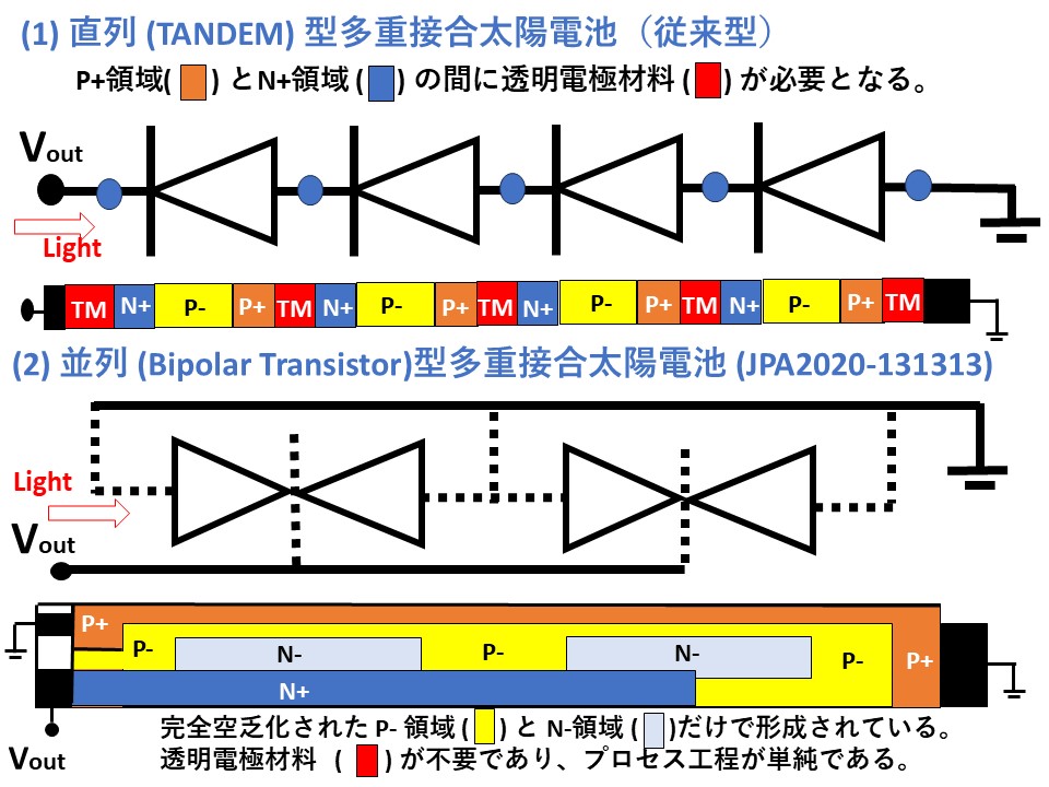
Abstract? The first silicon chip of a PP-NP-P+ double junction type solar cell
was fabricated for an AI self-energy robot vision application.
This PP-NP-P+ double junction photodiode is very attractive cost-wise.
We only need to add one high-energy ion implantation step to form the deep buried N type region and
another low-energy ion implantation step to form the surface P region.
The deep buried N type region is completely depleted,
to provide a free underground long channel for photo-electrons to be directed swiftly
to the small area N+P-P+ single junction outlet drain.
Subsequent steps are identical to the conventional single junction solar cell fabrication.
In external power-off mode, this AI self-energy robot vision chip,
with an image sensor array of N x M pinned-surface buried-channel
P+PNPP+ double junction type photodiodes can also function
as a solar cell energy source unit.
++++++++++++++++++++++++++++++++++++++++++++++++++++++
Publication_List_by_Yoshiaki_Hagiwara.html
2026_03_23_The_Difference_between_Hagiwara_JPA2020_131313_Multi_junction_Solar_Cell_and_Conventional_Tandem_Solar_cell.pdf
++++++++++++++++++++++++++++++++++++++++++++++++++++++
Mathematics_and_Physics_of_Semiconductor_Devices_by_Yoshiaki_Hagiwara_AIPS.pdf

Yoshiaki_Hagiwara_AIPS_Donation_Guide.pdf
Conribution_to_Global_High_Technology_Yoshiaki_Daimon_Hagiwara_AIPS.pdf

Conribution_to_Global_High_Technology_Yoshiaki_Daimon_Hagiwara_AIPS_1.pdf
Conribution_to_Global_High_Technology_Yoshiaki_Daimon_Hagiwara_AIPS_2.pdf
Publication_List_by_Yoshiaki_Hagiwara.html
++++++++++++++++++++++++++++++++++++++++++++++++++++++
++++++++++++++++++++++++++++++++++++++++++++++++++++++
Jump to Page 25
+++++++++++++++++++++++++++++++++++++++++++++++++++++++++
Hagiwara_AIPS_Laboratory.html
++++++++++++++++++++++++++++++++++++++++++++
Jump to Page
TOP_Page
001,
002,
003,
004,
005,
006,
007,
008,
009,
010
011,
012,
013,
014,
015,
016,
017,
018,
019,
020
021,
022,
023,
024,
025,
026,
027,
028,
029,
030
031,
032,
033,
034,
035,
036,
037,
038,
039,
040
041,
042,
043,
044,
045
+++++++++++++++++++++++++++++++++++++++++++