
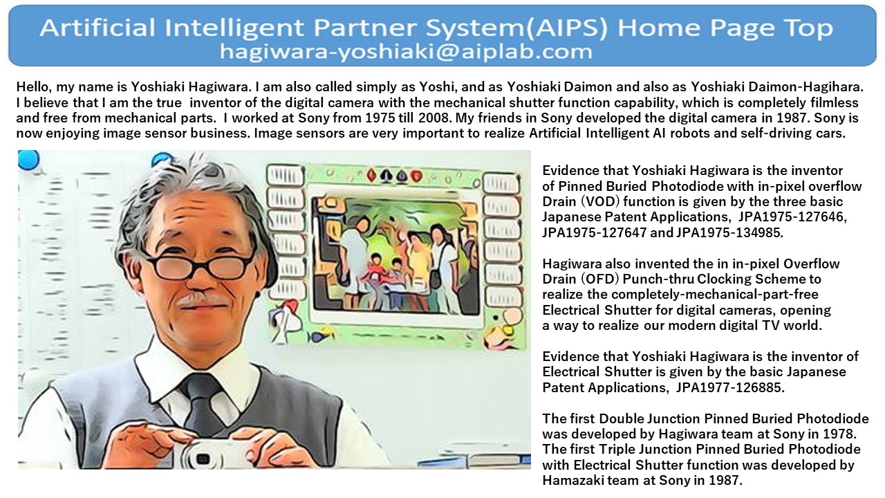


*********************************************
Updated at 9 p.m. on June 26, 2020 ( Japan Time )
*********************************************
hagiwara-yoshiaki@aiplab.com ( http://www.aiplab.com/ )
hagiwara@ssis.or.jp ( http://www.ssis.or.jp/en/index.html )
***************************************************
***********************************************
What is AIPS ( Artificial Intelligent Partner System ) ?
***********************************************

*******************************************************
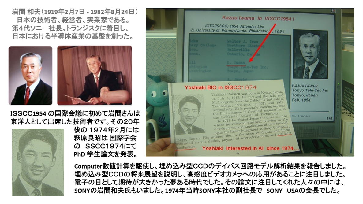
賢い撮像装置( Intelligent Image Sensor System)の研究です。
*******************************************************
監視カメラでの応用では、助けを必要とする人や泥棒さんの検出、
外科手術用内視鏡では、がん細胞群の検出などに期待されます・
(a) 画像信号による撮影制御(焦点制御技術、手ぶら補正技術等)
(b) 画像シーンの解析(構図抽出、被写体認識、撮影 Mode分析)
(c) 高解像化技術(ひずみ補正、HDR合成、超高解像化処理技術)
(d) 画像加工技術(画像をマンガ化、人の顔を似顔絵にする技術等も)
(e) 画像合成技術(パノラマ合成技術、特殊効果技術など)
(f) Refocus 技術(ぼけた映像や文字情報をはっきりさせます)
(g) 符号化開口などの特殊技術の構築等
いろいろな技術検討項目があり大変な総合技術力が不可欠です。
スマホ、自動運転車、ロボットなど応用され、現代文明の基盤に
とって、不可欠のものとなっています。これは日本の将来を豊かに
する産業です。その産業の活性化と発展のために、政府も企業も
是非、全力で取り組み、その未来に投資していただきたいです。
萩原にも、お金をください(笑顔)。
萩原 良昭
****************************
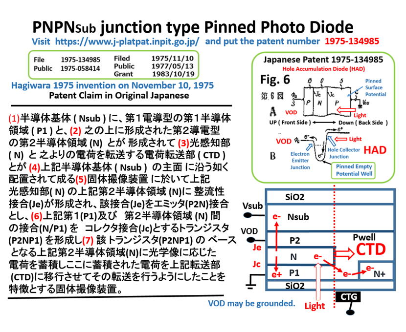
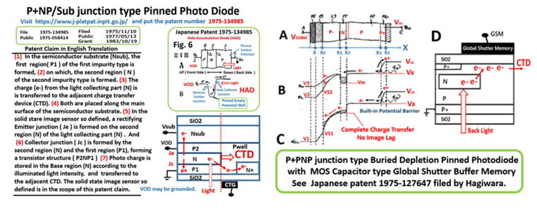
萩原考案の1975-127647 特許では、
この埋め込み電荷蓄積部のP+層の電位に注目した、かつ受光表面がN+層で
ピン留され、かつ、世界初の考案のGLOBAL SHUTTER機能と裏面照射型
を持つDynamic Photo Transistor の動作原理を明らかにした。
萩原の1975-134985 特許では、
この埋め込み電荷蓄積部のN層の電位に注目した、かつ受光表面がP+層で
ピン留された VOD 機能を持つ Dynamic Photo Transistor の
動作原理を明らかにした。
****************************
Hagiwara wrote a book on the AIPS digital circuits world.
Yoshiaki Hagiwara wrote a book on "the World of Artificial Intelligent
Digital Circuits",
which is important and needed to built the intelligent image sensor systems.
ISBM978-4-88359-339-2 ( Hard Cover, 460 page, 9000 Japanese Yen + tax )
If you are interestied in the book, Please visit
https://www.seizansha.co.jp/ISBN/ISBN978-4-88359-339-2.html
https://www.seizasha.co.jp/

*********************************************************


● 2019年10月開催の3次元集積回路の国際会議 3DIC2019 での発表論文です。
3DIC2019 Conference Paper at Sendai, Japan 2019
●2019年3月開催の半導体生産技術の国際会議 EDTM2020 での発表論文です。
EDTM2020 Conference Paper at Penang, Malaysia 2020
**********************************
****************************
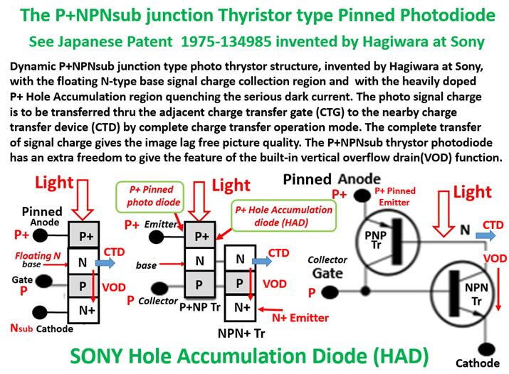
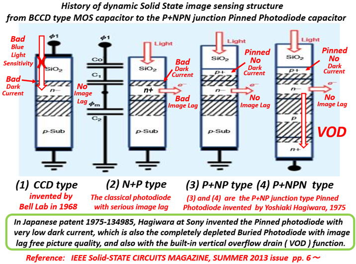
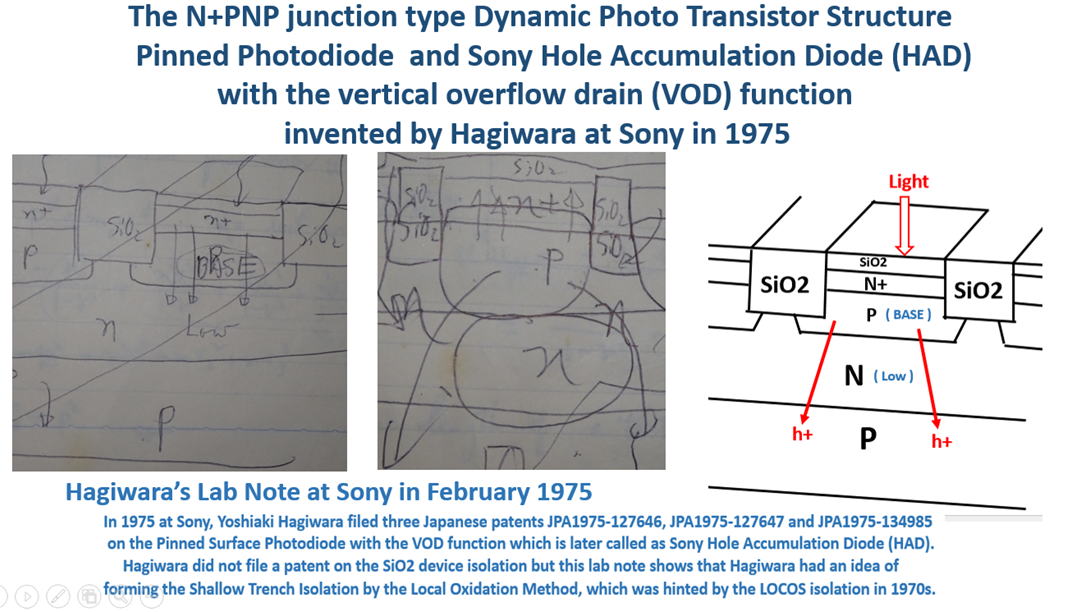
萩原の1975年の発明は、基板(Nsub)にP+NP接合トランジスタ型の
受光素子を形成するという発明でした。結果としてP+NPNsub接合型
のサイリスタ構造となります。実際はは、表面が P+P型の濃度勾配
を持つ、 Hole Accumulation Diode (HAD) 構造の提案でした。
(1) まず、最高の短波長青色光の感度、超光感度の特長を持ちます。
Image Sensorが 超感度なのは この受光素子構造だからです。
(2)表面が P+層でピンとめされた Pinned Photodiodeです。
表面電圧が固定され、シリコン結晶内は安定した動作が可能です。
みなさんが 車の中にいても、大雨で雷が鳴っていても安全ですね。
このP+で表面や周辺がピン止めされ、GNDに接地されると、
このP+NP型の受光部 N 層が守られ、表面暗電流雑音や
リーク電流がすくなくて、雑音の少ない,、きれいな映像を提供します。
(3) 電荷蓄積部は 埋め込み N 層なり、埋込み電荷蓄積部の中
の光電子は、隣接する電荷転送装置(CTD)に完全空乏化電荷
転送されます。すなわち、光電子の取り残しのない形で完全に
光電子が全部最後の1個まで転送されます。その結果、映像
には残像がありません。高速アクション撮影が可能となります。
(4) さらに、この発明は 結果として、 NPNP接合のサイリスタ―
構造型の受光素子ですので、いろいろな、NPNPサイリスタ―
としての動作は、NPNとPNPトランジスタの動作も、NP型の
ダイオードや PN型のダイオードの動作まで、期待できます。
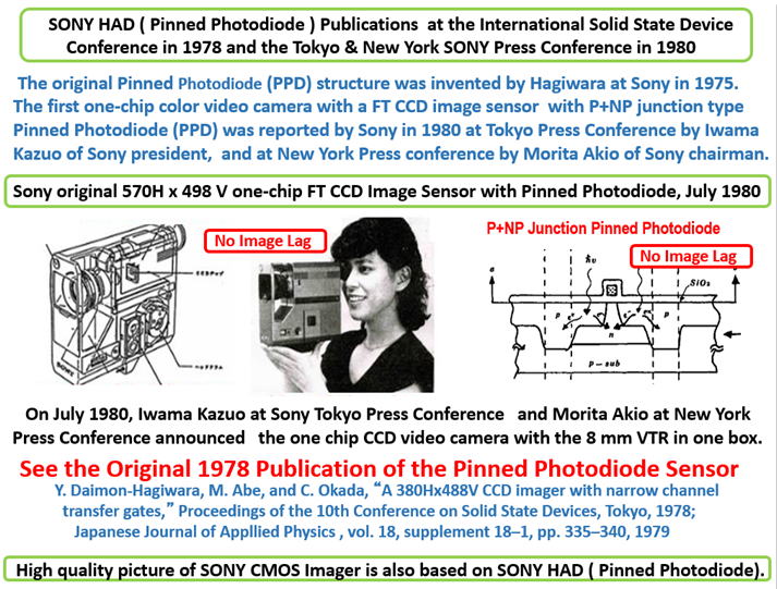
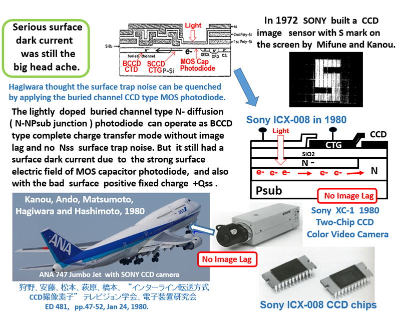
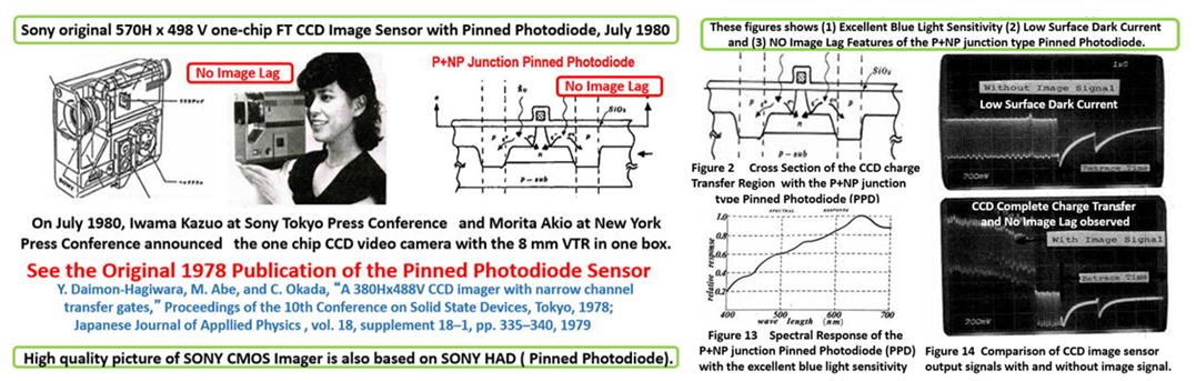
The first Image Lag free FT CCD image sensor
with the PNP junction type Pinned Photodiode was
reported at SSDM1978 by Yoshiaki Hagiwara at Sony.
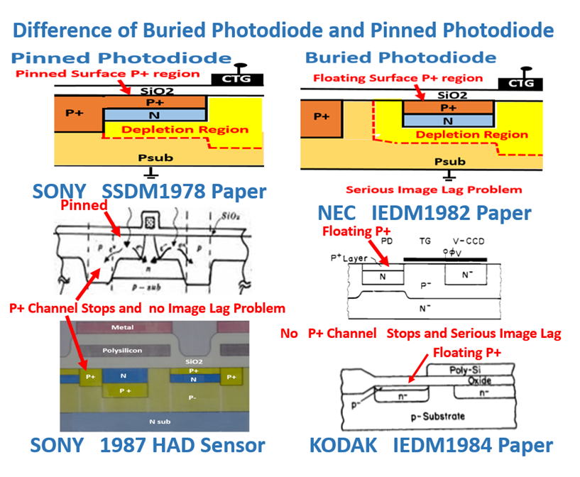
The first Image Lag free ILT CCD image sensor
with the PNPN junction type Pinned Photodiode
and the VOD electrical shutter function was
reported in the Journal of Nikkei Microdevices,
October 1987 Issue by Masao Hamazaki at Sony.
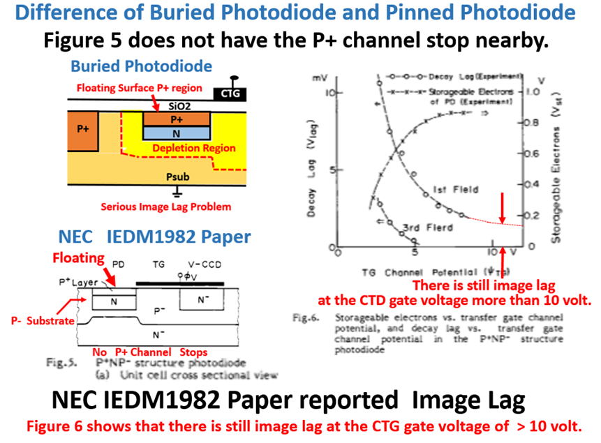
NEC IEDM1982 paper reported the image lag data.
The image lag is due to the RC delay of
the floating surface P+ layer ?
The details are explained below :
http://www.aiplab.com/Pinned_Photodiode_must_have_a_heavy_doped_Channel_Stops.pdf
*************************************
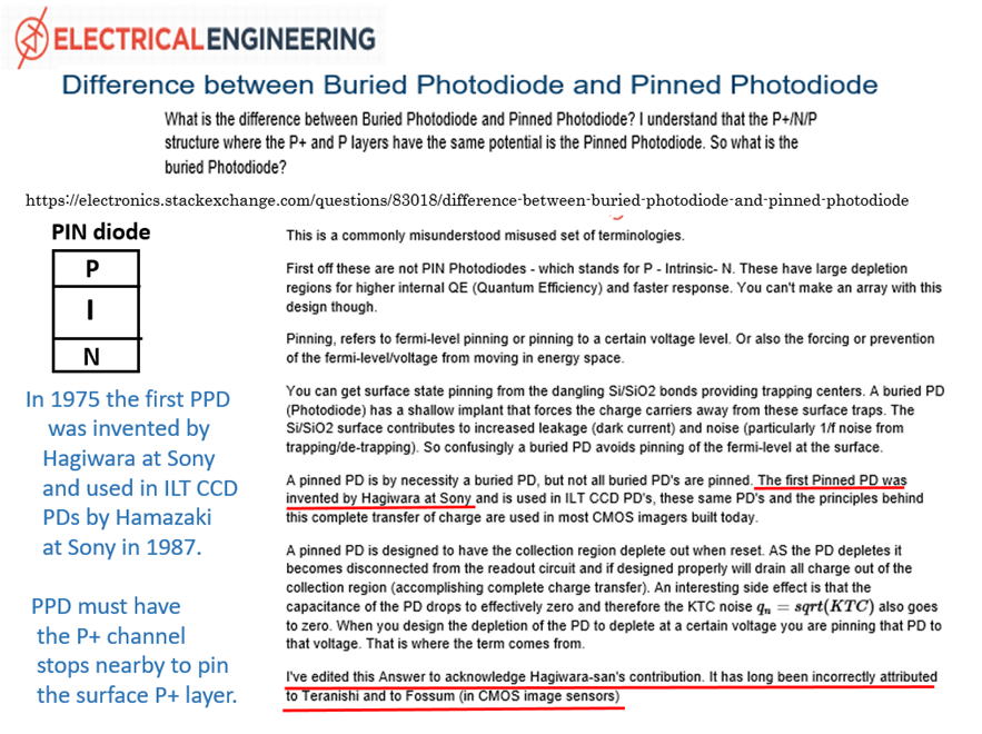
What is Pinned Photodiode (SONY HAD) ?
*************************************
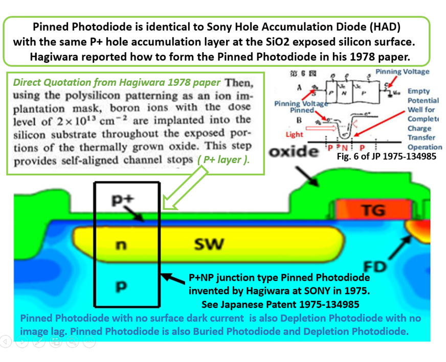
Pinned Photodiodeは必ず表面のP+がピン止めされている
固定電圧に固定される必要があります。そばに濃いP+の
完全に空乏化しない Channel Stops領域がないと埋め込み
N層の空乏層領域がぐるっと表面のP+層を包み込んで最終
的に表面のP+の空乏層が基板のP領域と電気的に分離
されて浮遊状態になる可能性があり動作が不安定となります。
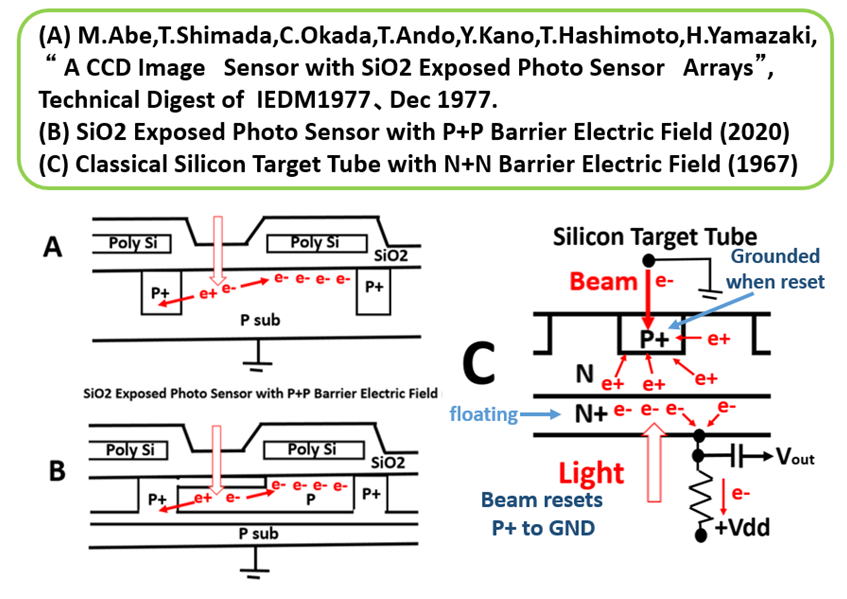
古典的な N+P接合型の場合は、N+領域が浮遊状態と
なり、残像が生じるのが大問題でした。
Pinned Photodiodeは必ず表面のP+がピン止めされている
固定電圧に固定される必要があります。固定されていないと
浮遊状態となり電荷が完全に埋め込みN層から隣接する
電荷転送電極(CTG)からは電荷が完全に吸い取ることは
不可能です。必ず残像が生じることになります。
また、表面のP+が固定されていないので表面に電界が
生じて暗電流が発生します。
太陽電池の場合は、この暗電流も、実際には、むしろ、反対に
熱エネルギ(kT)を電気に変換してくれるもので悪さはしません。
しかし、Image Sensorではこの暗電流は雑音として
観察され、暗い画面はすりガラスを通して見るような
映像になり、たいへん見苦しい画面となります。
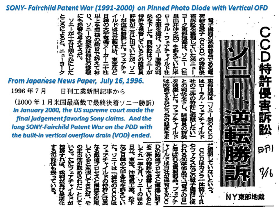
世界ではじめてPNP接合トランジスタ型のPinned Photodiode
を発明したのは萩原です。1975年の発明です。
萩原はまた、世界ではじめて、PNP接合トランジスタ型のPinned
Photodiodeの原理試作に成功しています。その構造には必ず
濃いP+の Channel Stops 領域が 絵素内に隣接して形成されて
います。P+層の近傍に P+ Channel Stops領域が存在する事
はこの Pinned Photodiodeが正常に安定して動作するために
は不可欠です。そばに P+ Channel Stopsが存在しないのは
本当の意味では Pinned Photodiodeと呼ぶことはできません。
*************************************
Hagiwara 's early contribution to the image sensor world.
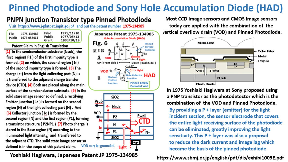
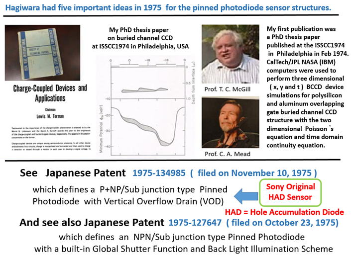
Japanese patent 1975-134985
on the P+NP junction photodiode on N substrate.
*************************************************
***************************************
This is the original 1975 Japanese Patent
on the SONY Hole Accumulation Diode (HAD).
***************************************
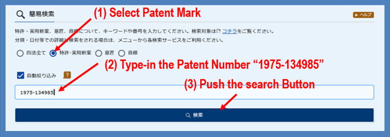
Original Paten Claims described in Japanese Language,
To get the Original Patent Claims described in Japanese Language,
please visit Japanese Patent Office Web Site.
https://www.j-platpat.inpit.go.jp.
(1) Select the Patent Mark
(2) Type in "1975-134985" and push the search botton.
Original Patent Claims translated in English Language,

https://www.shmj.or.jp/english/pdf/dis/exhibi1005E.pdf
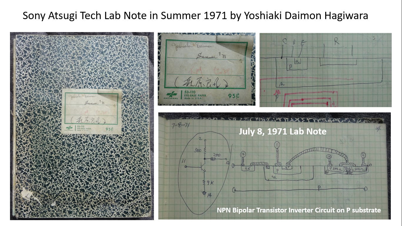
This is a very old forgotten patent of mine filed in November 10, 1975.
Hagiwara filed two more Japanese patents before this JAP1975-134985.
They are JAP1975-127646 and JAP1975-127647. These two patents
were intended to be applied in the three dimensional image sensor system
with the back light illumination scheme and the MOS buffer memory
for the global shutter function which is very much needed in the modern
three dimensional high performance CMOS image sensor structures.
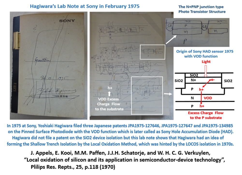
Imediately after Hagiwara joined SONY on February 20, 1975, with a
very fresh idea, Hagiwara filed these three basic patents on Pinned
Photodiode and SONY HAD concept.
Hagiwara forgot completely the details of these patents and did not
disclose the details to the international community. And no one
including Hagiwara himself did not pay atention to these patents.
****************************************
Sorry, it was all Hagiwara's problem making so
much confusions to the image sensor world.
****************************************
Recently Hagiwara published in the 3DIC2019 conference a paper titled
"Multichip CMOS Image Sensor Structure for Flash Image Acquisition"
******************************************************
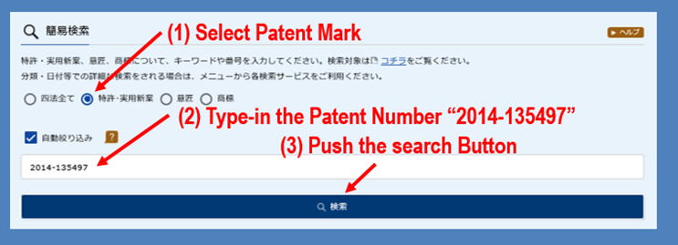
This is the most recent Hagiwara 2014 Japanese Patent Idea
Japanese patent 2014-135479
on 1/N sampling hold fast frequency Transfroamtion Method.
*****************************************************
To get the Original Patent Claims described in Japanese Language,
please visit Japanese Patent Office Web Site.
https://www.j-platpat.inpit.go.jp.
(1) Select the Patent Mark
(2) Type in "2014-135479" and push the search botton.
(1) Design and Performance Estimation
of DFT Processing Circuits ................ Student Paper 2014

(2) Digital Frequency Transformation Circuit
for Time-wise Unequally Sampled Data ......... Student Paper 2015
Japanese Patent JP2014-135497

*********************************************
"the World of Artificial Intelligent Digital Circuits",
***********************************************************
Hagiwara wrote a book on "the World of Artificial Intelligent Digital
Circuits",
which is important and needed to built the inteligent image sensor systems.
The book reviews first the elementary mathematics needed to understand
the basics of Semiconductor Device Physics and Digital Cirucuit Design
needed to construct an Artificial Intelligent Partner System (AIPS) using
the intellignet machine vision chips and powerful micro coltrol chips.
https://www.seizansha.co.jp/ISBN/ISBN978-4-88359-339-2.html
If you are interestied in purchasing book, please visit
https://www.seizasha.co.jp/ .
ISBM978-4-88359-339-2
( Hard Cover, 460 page, 9000 Japanese Yen + tax )
*******************************************
Many Basic Ideas of Semicondutor Device
and Digital Circuits are explained in details.
*******************************************

![]()

![]()
**********************************************************
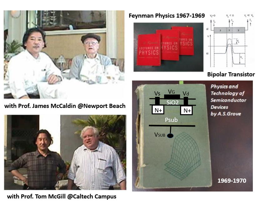
My Old Wonderful Memory Pictures
**********************************************************
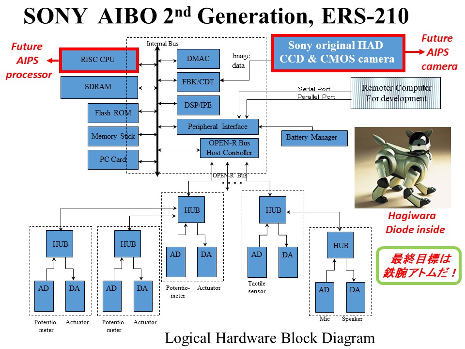
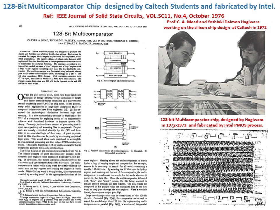
This 128 bit multi comparator was designed by Caltech students
including Hagiwara under the guidance of Prof. C. A. Mead and
fabricated in Intel Fab Line. This may be historically the first
univeristy and company colaboration example in the world.
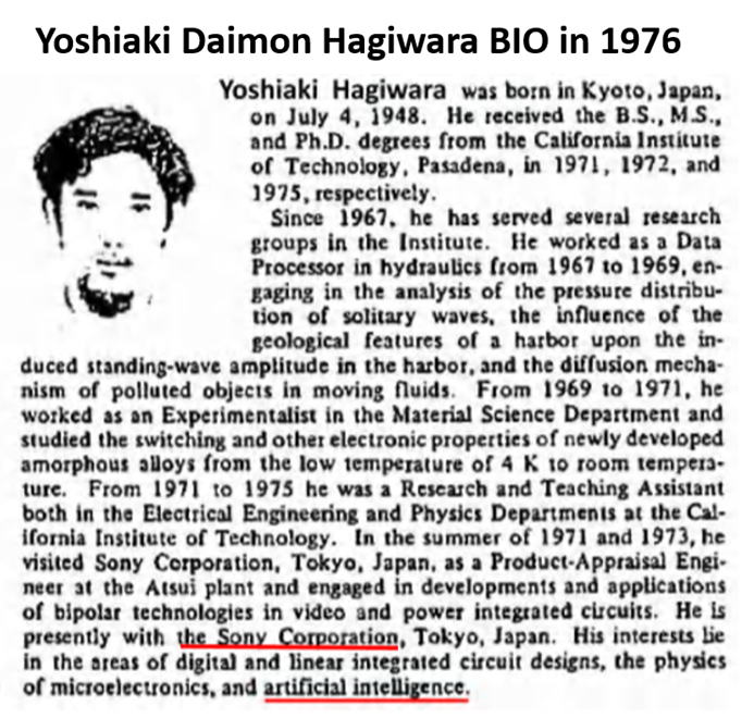
Hagiwara Bio in 1976 shows that Hagiwra was very much interested
in the artificial intelligent partner system (AIPS). Intel is also very
much interested in AI. Intel means intellignece, intelligent chips.....
In early 1970s, when IBM scientist described the MOS scaling
rule in IEDM conference. Dr.Gordon Moore predicted the growth
rate of his company (Intel) according to this scaling rule. And
Prof. C. A. Mead named Moore's preidction as the Moore's Law.
Hagiwara was a student of Prof, C. A. Mead and immediately
understood this Moore's Law. But Hagiwara found out that,
to have the active circuits in the small picture element area
of image sensors, Hagiwara had to wait till the 21 century.
Hagiwara could not wait and thought the CCD is the savior
meanwhile, until CMOS technology becomes well advanced.
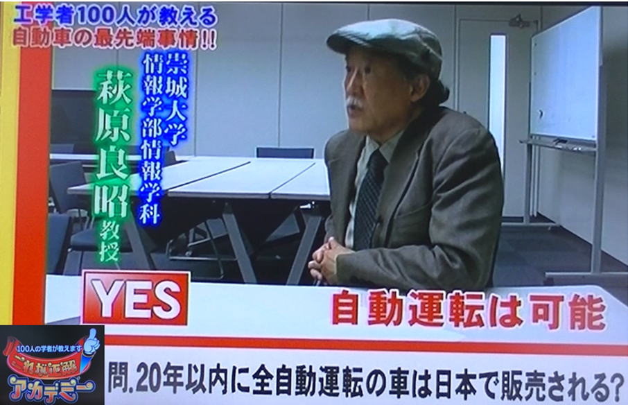
*******************************************
Hagiwara Yoshiaki on Fuji TV Japan Network,
commenting on Future Self Driving Car
with Artificial Intelligent Partner System (AIPS)
*******************************************
***********************
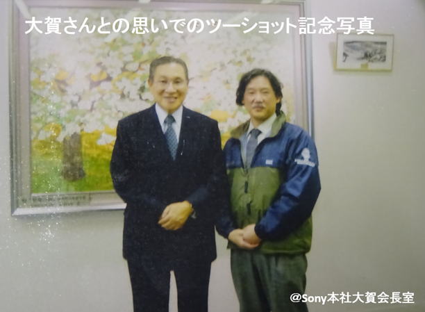
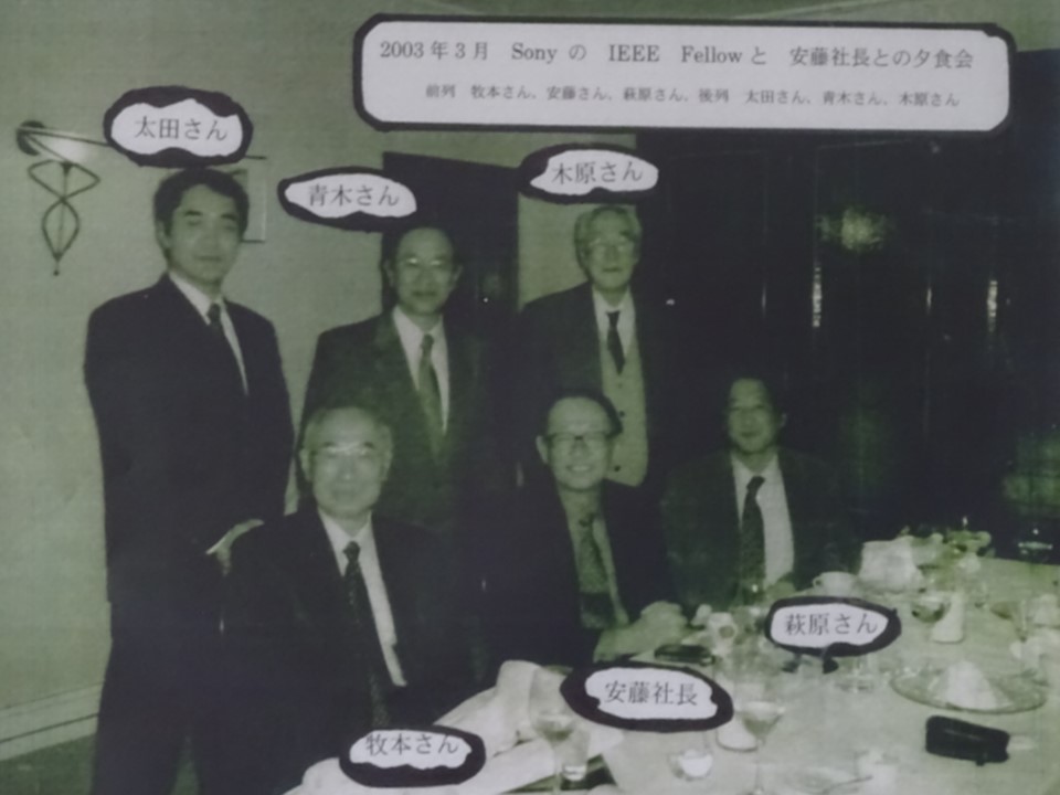
大賀会長室の壁にはお気に入りの大きな花の絵が飾ってありました。
中村末廣副社長と一緒に呼ばれて行きました。
大賀会長と和やかに会話がはずみ楽しいひと時でした。
写真は中村末廣副社長のご好意で撮っていただいきました。
大賀さんとの思い出のツウショット写真です。
***********************
今のSONYの働き頭は Playstation と Image Sensor のビジネスです。
大賀さんに当時久夛良木さんと萩原は守っていただきました。
大賀さんは久夛良木さんにとっても萩原にとっても大の恩人でした。
大賀さんのお蔭で今のSONYはあると言っても過言ではありません。
大賀さんに感謝、感謝です(萩原良昭)。
***********************
********************************
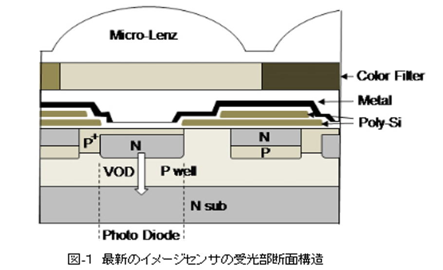
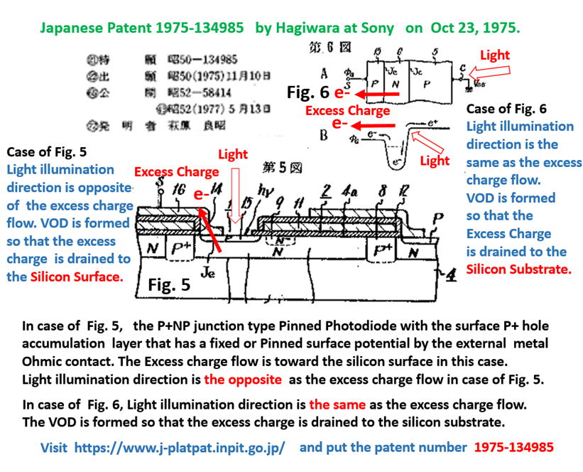
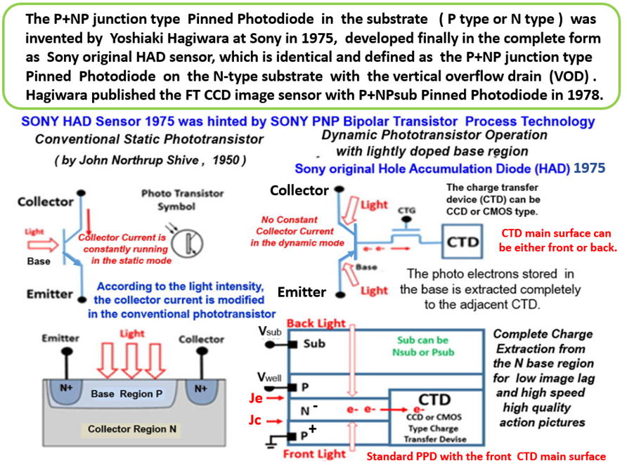
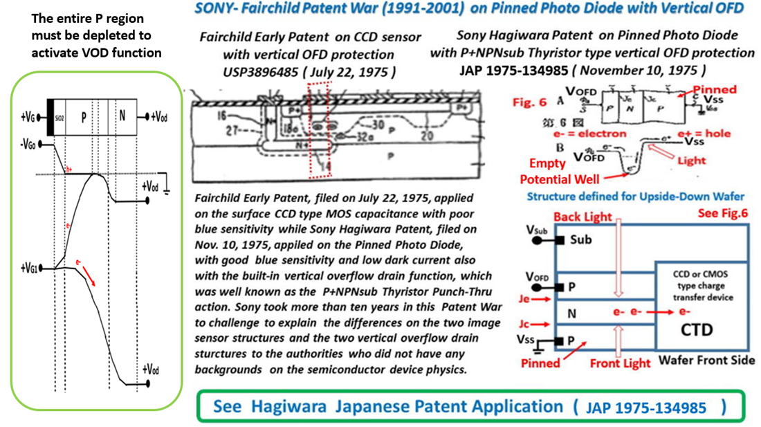
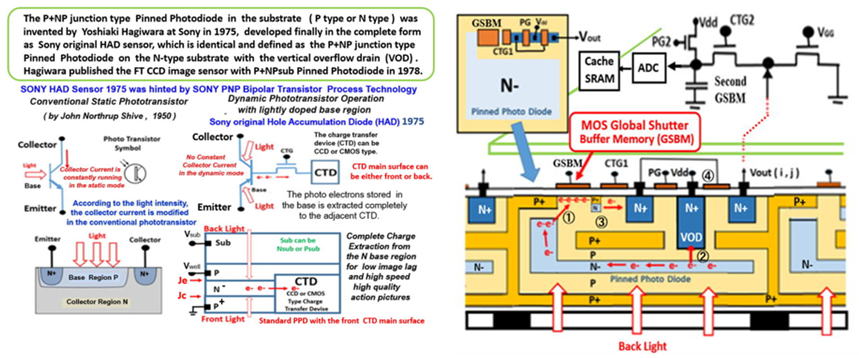
垂直 Overflow Drain (VOD) 機能を持つ受光素子 の発明
********************************
<日本国特許 1975-134985 > 萩原良昭
N型基板のPウエルにPN接合フォトダイオードを形成し、N層直下のP層を
空乏化(パンチスルー状態)にすることで、過剰電子をN層からN型基板に
すべて掃き出す、縦型オーバーフロードレイン(VOD)機能を持つ構造を
萩原は、世界で初めて、考案発明した。< 特許1975-127647 >
**********************************
***** 残像のない受光素子 (Pinned Photodiode) の発明 *****
<日本国特許 1975-127647 > 萩原良昭
電荷転送装置(CTD)からなる、外部回路への転送ゲートの電位の関係を
萩原は、世界で初めて、特許 1975-127647 で、空乏化したN層の電位
を転送ゲートのチャネル電位より所要値以上に高く保ち、信号電荷を、
完全に空乏化電荷転送して、残像の発生しない、動作原理を明示した。
**********************************
![]()
****** Global Shutter 機能を持つ受光素子 の発明 ********
<日本国特許 1975-127646, 1975-127647 > 萩原良昭
萩原は、世界で初めて、立体三次元構造に適した、裏面照射型の受光素子、
であり、埋め込み型のPhotodiode でもあり、かつ、Pinned Photodiodeでも
ある超感度超高性能な受光素子を1975年に既に発明していた。その構造は、
現在の CMOS Image Sensor には不可欠な、Global Shutter 用のMOS 型
のBuffer Memoryを各絵素に組み込んだ、優れた性能を持つ受光素子である。
**********************************
****************************
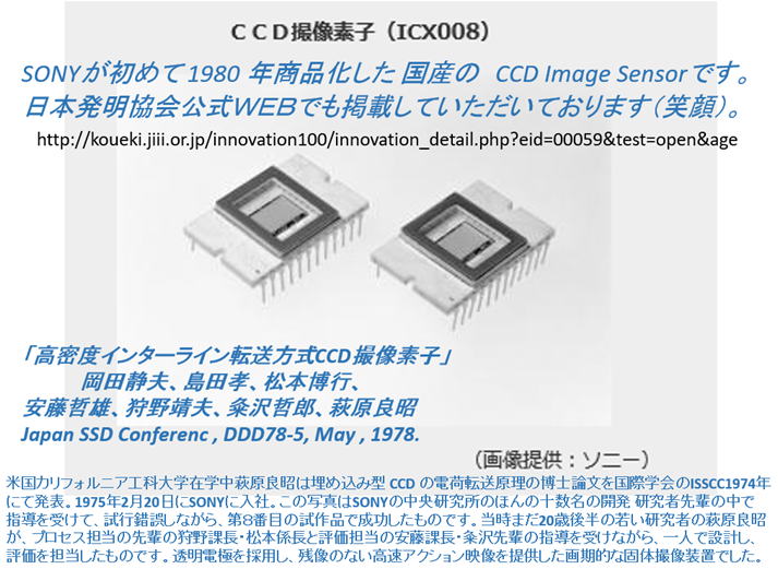
●Innovation 100 掲載記事
****************************
http://koueki.jiii.or.jp/innovation100/
****************************
●Image Sensor 記載記事
****************************
イメージセンサー(CCD・CMOS)
****************************
参考文献
*******************************
(1)W. S. Boyle and G. E. Smith 「Charge Coupled Semiconductor Devices」,
The Bell System Technical Journal, vol.49 (1970) pp.587-593
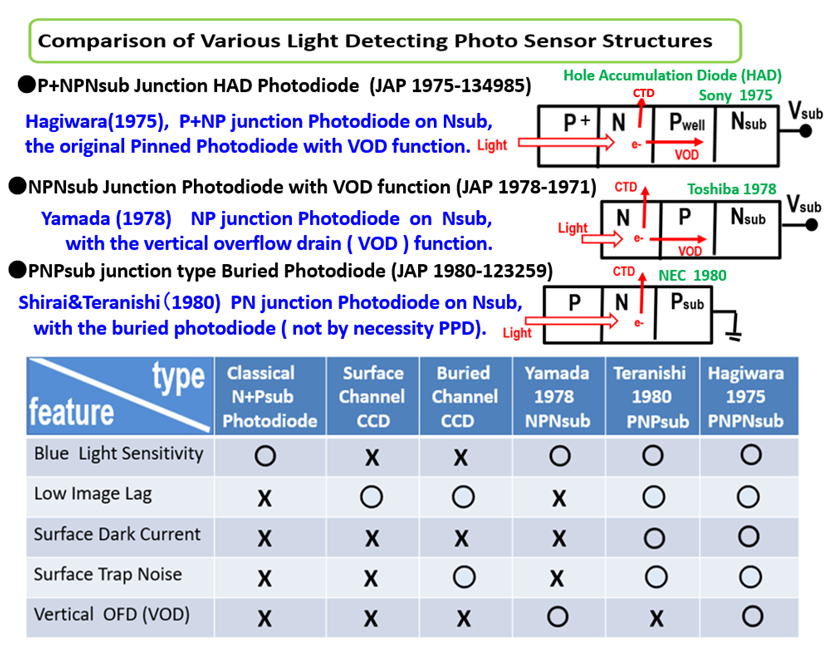
(2)山田哲生「固体撮像装置」特開昭54-95116、1978年1月13日出願
基板(N)に NP接合を形成した受光素子の提案である。表面のN層を
光電子の蓄積部としている。かつ、基板(N)に過剰電子を流し出すもので、
縦型OFD(VOD)機能を実現するNPN接合構造の受光素子の提案である。
(3)寺西信一ほか「固体撮像装置」特開57-62557、1980年10月2日出願
基板(P)に PN接合を形成した受光素子の提案である。光電子の蓄積部
を埋め込みN層とする、埋込みPhotodiode型の受光素子の提案である。
(4)米田智也ほか「固体撮像装置」特開2001-230400、2000年11月30日出願
強い光が入射したときに発生するシェーディングを抑制する構造を発明。
(5)鈴木亮司ほか「X-Yアドレス型固体撮像素子およびその製造方法」
特開2003-31785、2001年7月11日出願、裏面照射型に関する発明。
(6)梅林拓ほか「半導体装置とその製造方法、及び電子機器」
特開2015-65479、2010年1月22日出願、メージセンサーに画像処理
回路を積層する構造を発明し高速化と多機能化を飛躍的に推し進めた。.
,
もうひとつ、関連特許として、このP+NP接合型 Pinned Photodiodeで、
注目すべき特許、受光素子の特許が1977年に日立(小池ほか)があります。
**************************
萩原の1975年出願の基本特許と1978年の学会発表は
世界最初の Pinned Photodiodeの考案です。
**************************
*************************
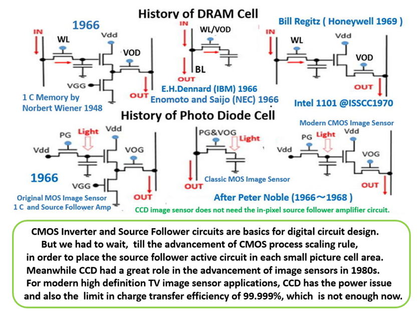
Image Sensorは感度が命である。感度はS/N決まる。
CCD型電荷転送装置は長い間超低CLOCK配線CkT雑音
素子として貢献しImage Sensor の発展に寄与してきた。
しかしCMOSプロセスの微細化によりImage Sensor
の限られて単位絵素面積にもMOS Transistor 回路
が組み込める時代となり絵素ごとに in pixel active
Source follower amp 回路が組み込め、CMOS型電荷
転送装置がCCD型電荷転送装置より消費電力と実行
的な電荷転送効率でも有利となりCCD型電荷転送装置
はもはや Image Sensor の主要部品の座から降りる
事になった。
しかし、萩原が1975年に考案した Pinned Photodiode、
PNP接合トランジスタ型の受光素子はCCDの時代から
現在のCMOS Image Sensorでも、超感度低暗電流
雑音特性を持ち、さらに残像のない特性を発揮し
高速撮影やアクション撮影を可能にするVOD機能や
電子shutter機能も萩原の1975年の発明である。
さらに萩原は3次元構造に不可欠な裏面型のImage
Sensorを1975年にすでに考案した。またそれだけ
でなく、CMOSに不可欠な GLOBAL SHUTTER機能
用のMOS容量型 in pixel buffer memoryも各
絵素に組み込みことを1975年の特許で考案した。
その1975年の萩原のアイデアのPNP接合型
受光素子の動作は1978年の原理試作で実証
確認された。それが今のImage Sensorの原型
Mother となった。
************************
***************************
●1975年に出願して3件の PNP接合 double juncton 型の
Pinned Photodiodeの受光素子の基本特許です。
JPA 1975-127646, JPA 1975-127647 and JPA 1975-134985
●SSDM1978で発表したもので、 PNP接合 double juncton 型の
Pinned Photodiodeの受光素子の世界最初の Original 論文です。
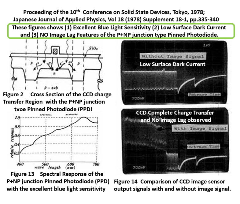
"A 380H x 488V CCD Imager with Narrow Channel Transfer Gates"
Proceeding of the 10th Conference on Solid State Devices, Tokyo 1978;
Japanese Journal of Applied Physics, Vol 18 (1979) Supplement 18-1,pp.335-340
●10月の論文は萩原の1975年の発明は裏面照射型で
3次元集積回路の適した受光素子構造である事を強調
した論文でした。
“Multichip CMOS Image Sensor Structure for Flash Image Acquisition”
at the IEEE sponsored 3DIC2019 conference at Sendai Japan in October 2019.
http://www.aiplab.com/P2019_3DIC2019Paper_on_3D_Pinned_Photodiode.pdf
●またこの3月の論文はご存知の様に半導体生産技術の
国際会議で従来のPinned Photodiode(別名 SONYの
HAD)は 受光構造が P+NP接合ではなく、実際は
表面イオン打ち込みによるガウス関数分布となり実質
はP+P表面濃度勾配をもち、このP+P濃度勾配に
よりバリア電界が表面での青色感度の向上に寄与する
ことを説明しました。
“Simulation and Device Characterization of the P+PN+P Junction Type
Pinned Photodiode and Schottky Barrier Photodiode “,
http://www.aiplab.com/P2020_EDTM2020_PaperID_3C4_by_Hagiwara.pdf
*******************************
*******************************
萩原良昭の主要なAWARD 授賞の紹介
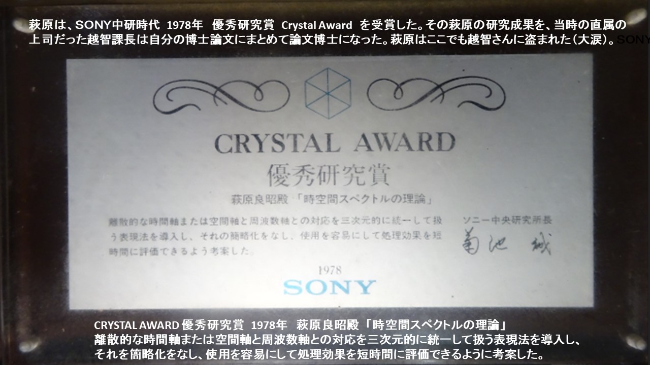
(1) SONY 中研時代には SONY 中研から CRYSTAL AWARDを受賞しています。
http://www.aiplab.com/Sony_Award_CrystalAward1978.jpg
(2) SONY社内での HAD( PPD)の社内での第1級特許褒賞記録と
http://www.aiplab.com/Sony_Patent_Award_on_Pinned_Phtodiode.jpg
(3) SONY社内での VOD付きPPDの電子SHUTTERの特別褒賞記録です。
http://www.aiplab.com/Sony_patent_Award_on_Electric_Shutter_HAD.jpg
(4) SONYは CELL PROCESSORでも GROUP AWARDを
貢献者の一人として受賞しました。
http://www.aiplab.com/PS3_Cell_Proceesor_Sony_Team_Award.jpg
(5) また長年 ISSS運営委員会のメンバーとして その貢献者の
1人としてService AWARDを受賞しています。
http://www.aiplab.com/ISSCC2003_Executive_Committee_Contribution_Award.jpg
萩原良昭の主要な学会論文の紹介
(1) SSISの公式 WEB サイトの記載記事
https://www.shmj.or.jp/english/pdf/dis/exhibi1005E.pdf
(2) 萩原の 1975年の3件の日本語特許出願
Japanese Patent 1975-127646 on N+NP+NP junction Pinned Photodiode
http://www.aiplab.com/JP1975-127646_A.jpg
http://www.aiplab.com/JP1975-127646.pdf
Japanese Patent 1975-127647 on N+NP+N junction Pinned Photodiode
http://www.aiplab.com/JP1975-127647_A.jpg
http://www.aiplab.com/JP1975-127647.pdf
Japanese Patent 1975-124985 on P+NPNsub junction Pinned Photodiode
http://www.aiplab.com/image7.jpg
http://www.aiplab.com/JP1975-134985.pdf
(3)1978年の萩原のSSDM1978の論文
http://www.aiplab.com/P1978_Pinned_Photodiode_1978_Paper_by_Hagiwara.pdf
(4)その内容を評価して翌年 1979年に受けた
Image Sensor Society 主催の国際会議
CCD79 Conference での招待講演論文
https://www.imagesensors.org/Past%20Workshops/1979%20CCD79/03-1%20Hagiwara.pdf
(5)ESSCIRC2001でも招待講演
http://www.aiplab.com/P2001_ESSCIRC2001.pdf
(6)ESSCIRC2008でも基調講演
http://www.aiplab.com/P2008_ESSCIRC2008Hagiwara.pdf
https://ieeexplore.ieee.org/document/4681786
(5)昨年10月のIEEE主催の3次元集積回路の
国際学会 3DIC2019 Conferenceの投稿論文
http://www.aiplab.com/P2019_3DIC2019Paper_on_3D_Pinned_Photodiode.pdf
(6)そして最後がIEEE主催のEDTM2020での投稿論文
http://www.aiplab.com/P2020_EDTM2020_PaperID_3C4_by_Hagiwara.pdf
*******************************
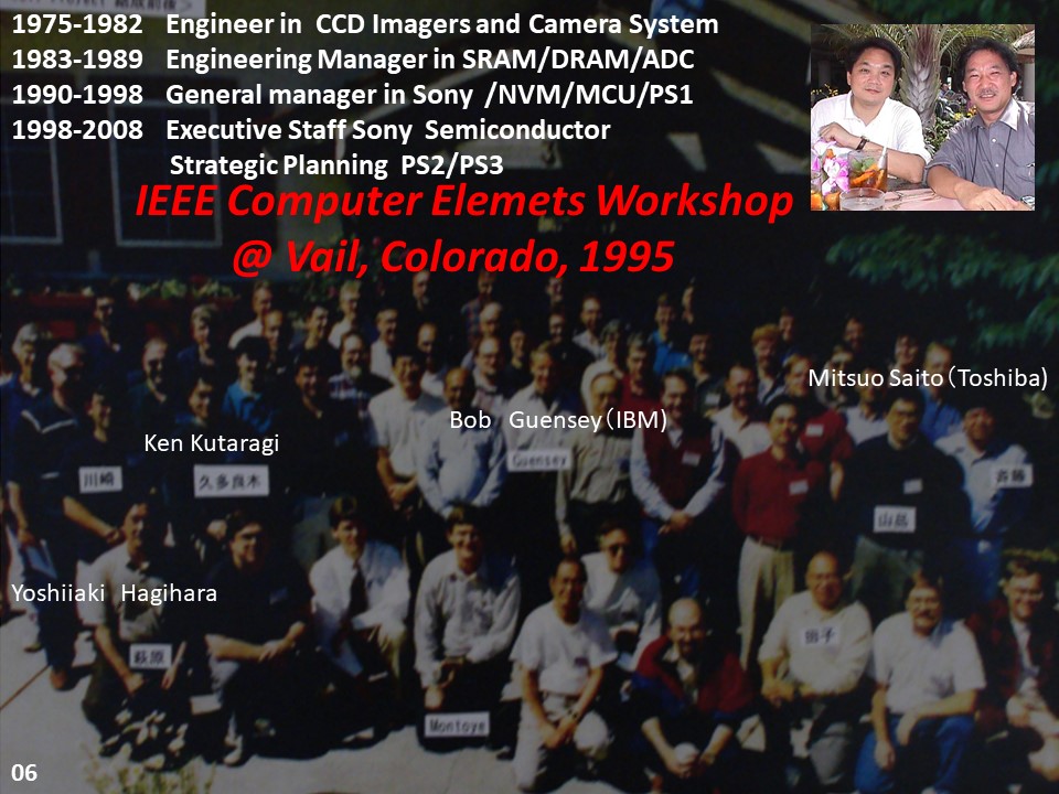
One invention was perfected by the ideas and efforts of
many diligent engineers and scientists. I worked for
image sensors in Sony only from 1975 till 1980. Then
I focused my attention to develop the digital camera
system LSI chips which was my life work in Sony.
I had a very wonderful time in Sony with many friends
working together with me, and still enjoying working for
future vision system chips for AI IoT Robotics world.
*********************************************************
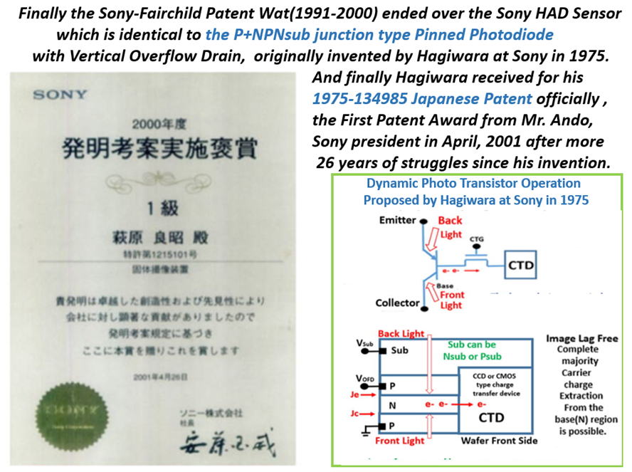
I have the basic patent 1975-128885 on the electrical shutter function
on the dynamic PNPN junction type photodiode which, as you know, later
became the basis of the PNP jucntion NEC and Kodak Pinned Photodiode
and the NPNP jucntion Sony Hole Accumulation Diode (HAD).
http://www.aiplab.com/Sony_patent_Award_on_Electric_Shutter_HAD.jpg
I was awarded internally in Sony by Idei san, Sony President and CEO,
for the invention of the Sony Hole Accumulation Diode with the vertical
overflow drain (VOD) function scheme for the 1977-128885 Japanese Patent.
These old patents of mine ( JP1975-124676, JP1975-127647, JP1975-134985
and JP1977-128885 ) were all written in Japanese and were never disclosed
to the international world in details and causing many misunderstandings.
At that time in 1970s, we never thought the importance of patent files.
We were very busy to build a good image sensor for our customer market.
It was all my fault that I never explained these important ideas of mine
in details in the international English Journal and publications.
But I strongly believe that I invented the dynamic photo transistor
with the excellent light sensitivity, the extremely low surface dark current,
the extreme low image lag, the in pixel overflow drain(VOD), and the in pixel
MOS buffer memory for the Global shutter operation which is essential
for modern CMOS image sensors. In 1975, I also had the idea of the back
light illumination scheme for the dynamic photo transistor which is very
promising for building the three dimensional (3D) multi stacked integration
for a high performance real time robot vision system.
http://www.aiplab.com/P2019_3DIC2019Paper_on_3D_Pinned_Photodiode.pdf
http://www.aiplab.com/P2020_EDTM2020_PaperID_3C4_by_Hagiwara.pdf
I believe my inventions served as the initiator to accelerate Sony, Kodak and
other companies to build the digital camera and change the world from the
analog life style of film media to the new digital life style for AI IoT Robotics
for the future.
*********************************************************
*******************************
What is Pinned Photodiode ?
Study Special Relativity Theory
What is Abura Wake Zan ?
Study Korean for Your Enjoyment
Enjoy C-programming.
Hagiwara Publication List
IEEE_EDS_Kansai_Chapter_IMFEDK2006_Hagiwara.pdf
DRAM_SRAM_Technology_and_Problems_1998_07_29_Hagiwara
Pinned_Photodiode_must_have_a_heavy_doped_Channel_Stops
*********************
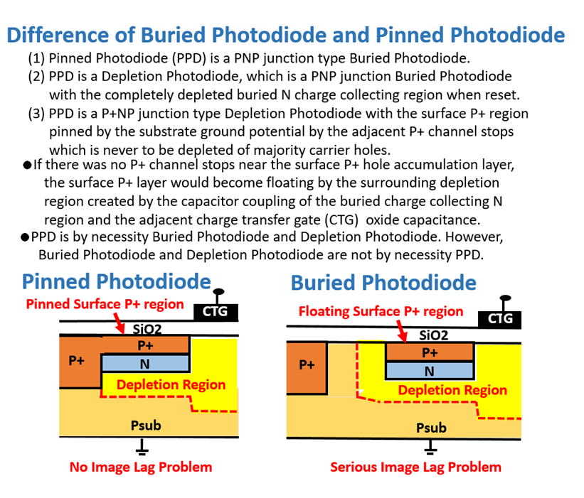
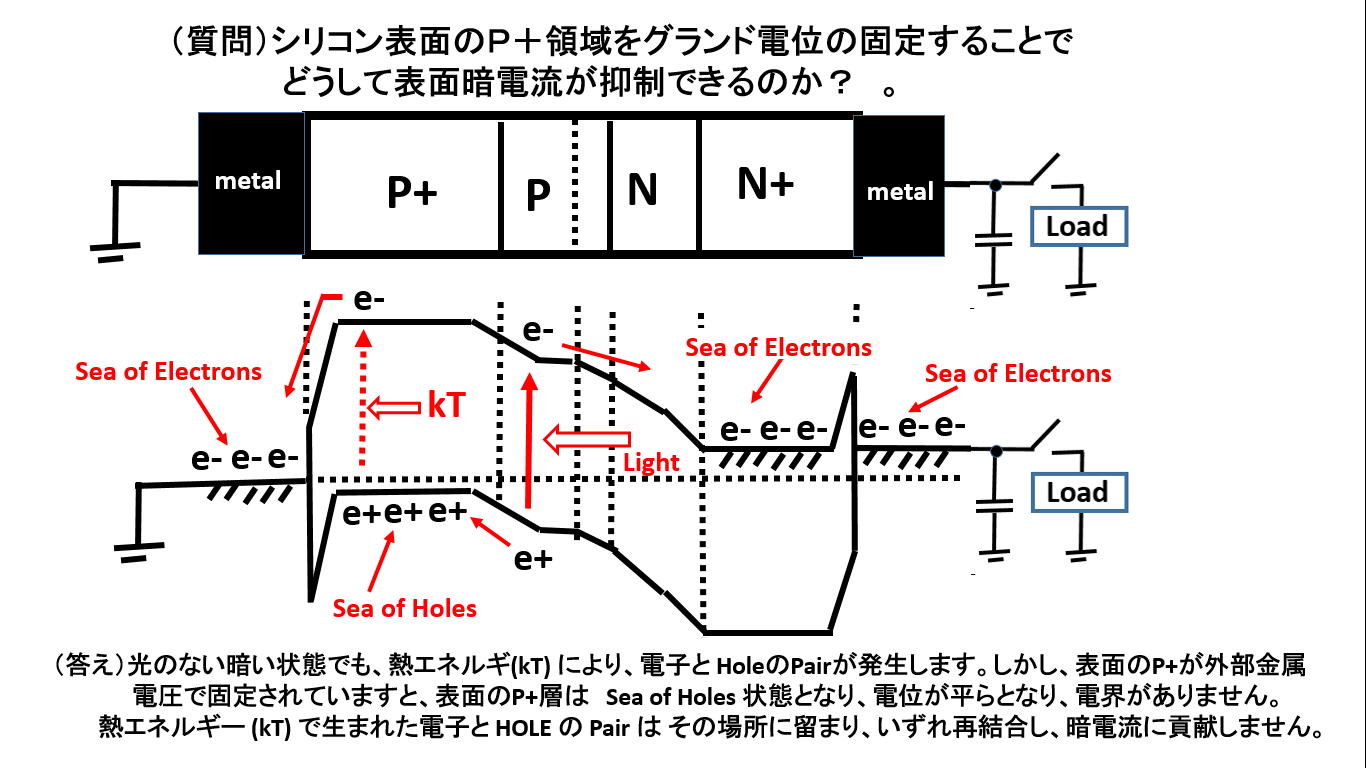
●まずPinned Photodiode は完全な埋め込みPhotodiodeでなければなりません。
不完全は完全な埋め込みPhotodiodeはバリアが生じ残像が発生します。
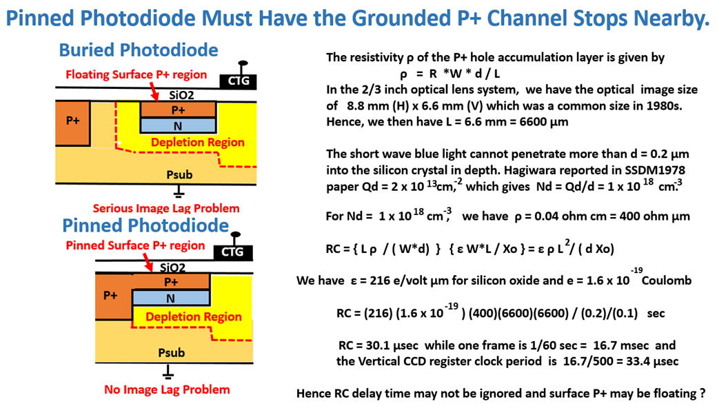
●Pinned Photodiode はP+ Channel Stops 領域が絵素の近傍になければなりません。
P+ Channel Stops 領域がないと受光部のP+ 層が RC 遅延を持ち電位がふらつき
浮遊状態(Floating)になり、その結果残像が生じます。
http://www.aiplab.com/Difference_of_Pinned_Photodiode_and_Buiried_Photodiode_1.jpg
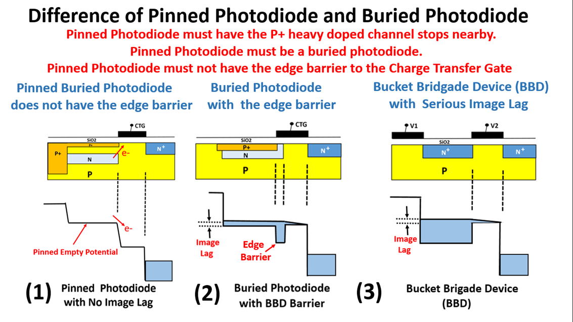
NECのIEDM1982の論文は上記の2つの問題が重なり残像があったと観察します。
NECのIEDM1982年論文も 1980年特許も PPD 特許ではありません。
世界の人々はほとんどの方々が半導体デバイス物理の専門家でないので
世界のほとんどの方々はこの重要な事実を理解できず誤解しています。
++++++++++++++++++++++++++++++++++++++++++++++++++++++++++++++++++++
Pinned Photodiode must have the heavily doped channel stops nearby
and also completely buried signal charge collection and storage N region.
++++++++++++++++++++++++++++++++++++++++++++++++++++++++++++++++++++
In 1975, Sony proposed the Pinned surface PNP and PNPN junction type
dynamic phototransistor with the in pixel vertical overflow drain (VOD)
function for light detecting devices.
In 1978, Sony introduced one chip FT CCD image sensor with the Pinned
surface PNP junction type dynamic phototransistor which then became
the primary photodetector for CCD image sensors.
In 1984 Kodak called the Sony original Pinned surface PNP junction type
dynamic phototransistor simply as Pinnned Photodiode.
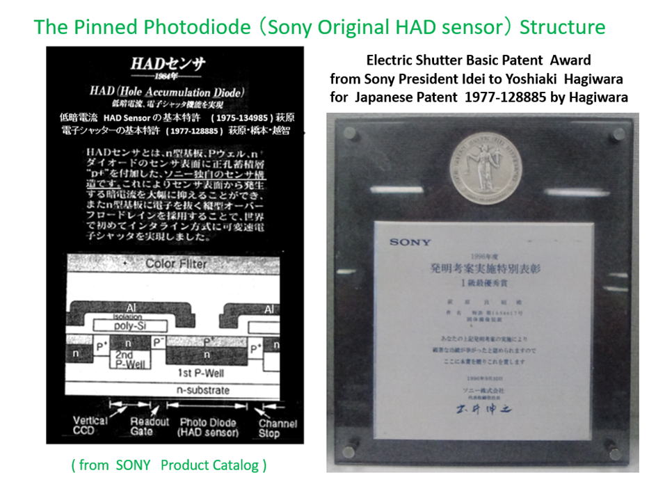
In 1987, Sony introduced a 2/3 inch, 380,000-pixel CCD image sensor
(ICX022) with the Pinned surface NPNP junction type dynamic Photo
Thryristor with VOD function which Sony then called simply as Hole
Accumulation Diode (HAD).
In the 1990s, the era of passport size video cameras demands compact
CCD image sensors with large numbers of pixels (1/2 inch or smaller
with 400,000 pixels or more).
In 1995, Kodak adopted Pinned Photodiode for CMOS image sensors.
Pinned Photodiodes, since invention by Sony in 1975, are still
the primary photodetector for CCD and CMOS image sensors now.
+++++++++++++++++++++++++++++++++++++++++++++++++++++++++
********************************
下記の発明協会の記載は事実誤認もはなはだしいです。
********************************
http://koueki.jiii.or.jp/innovation100/innovation_detail.php?eid=00059&test=open&age
***************************************
撮像デバイスの研究開発は、19世紀後期のテレビジョン研究がスタートである。
機械式、撮像管、固体撮像素子(以下「イメージセンサー」と呼ぶ)と発展し
社会に大きなインパクトを与えつつ、大きく発展してきた。
真空管の一種である撮像管は、サイズが大きい、割れ物である、消費電力が大きい、
画像にゆがみがある、高価である、などの欠点があり、固体化が望まれていた。
1960年代半ばにイメージセンサーの開発がスタートした。そのときは、MOS
(Metal Oxide Semiconductor)型が中心であった。
1970年にBoyleとSmith(当時Bell研究所)がCCD(Charge-Coupled Device、
電荷結合素子)を発表した (1)。構造が単純であり、イメージセンサーのような
大規模なアレイ構造を製造するのに適していること、矢継ぎ早にCCDに改善
が加えられたことから、イメージセンサー開発の中心はCCDになった。
1970年後半からは開発の中心は日本に移った。1978年、山田哲生(当時 東芝)は、
強い光が入射したときに縦線の偽信号を発生させるブルーミングを抑制する
縦型オーバーフロードレイン構造を発明した(2)。
●SONYの萩原はすでに特許 1975-134985 の中で VOD付きにPPDを発明しています!
1979年には寺西信一(当時 NEC)が、白傷や暗電流を大幅に低減し、残像や
転送ノイズを解消する埋込フォトダイオード(Pinned Photodiode)を発明した(3)。
●SONYの萩原はすでに特許 1975-134985 の中で (Pinned Photodiode)を発明した。
●この発明協会の記載は埋込フォトダイオードとPinned Photodiodeの違いを理解していない。
これらの結果、CCDはまずムービーを、引き続きコンパクトデジタルスチル
カメラを主な市場として量産されていった。
1990年代になると、CMOSの微細化が進み、4個ほどのトランジスターを
画素内に配置することが可能になり、さらには、埋込フォトダイオードを
CMOSイメージセンサーに適用することでCCDと同等以上の低ノイズが
達成でき、世界の多くの機関で熱心に開発が進められた。
●画素内に4個ほどのトランジスターを配置する In Pixel Active Sensor
はすでに1960年代に Intel社が 3T1C から 1T1C DRAMの商品化を
進めている時に 英国の Peter Noble が考案していた。
2000年に米田智也ら(当時 キヤノン)が、強い光が入射したときに
発生するシェーディングを抑制する構造を発明した)4)。
2001年に鈴木亮司ら(当時 ソニー)が、裏面照射型に関する発明をした(5)。
●萩原はすでに 特許1975-127646 と 特許1975-127647 で裏面照射型PPDを考案した。
これらの技術開発によりCMOSイメージセンサーが主役になり、低消費電力
という特性のお陰もあり、携帯電話に搭載され、生産量を爆発的に増加させて
いった。2010年に梅林拓ら(当時 ソニー)が、イメージセンサーに画像
処理回路を積層する構造を発明し(6)、高速化と多機能化を飛躍的に推し進めた。
2014年には携帯電話用を中心に約38億個もの生産が行われた。パソコンカメラ、
デジタルスチルカメラ、ゲームなどのコンシューマー用途、監視用、車載用、
放送用カメラなどの社会インフラとして、さらには医療、科学用などあらゆる
ところでイメージセンサーが使われるようになった。
**************************************
参考文献等
1. W. S. Boyle and G. E. Smith 「Charge Coupled Semiconductor Devices」,
The Bell System Technical Journal, vol.49 (1970) pp.587-593
2. 山田哲生「固体撮像装置」特開昭54-95116、1978年1月13日出願
3.寺西信一 外「固体撮像装置」特開57-62557、1980年10月2日出願
4.米田智也 外「固体撮像装置」特開2001-230400、2000年11月30日出願
5.鈴木亮司 外「X-Yアドレス型固体撮像素子およびその製造方法」
特開2003-31785、2001年7月11日出願
6.梅林拓 外「半導体装置とその製造方法、及び電子機器」
特開2015-65479、2010年1月22日原出願
**************************************
![]()
*********************
Slide2020_05_31
Slide2020_06_10
Slide2020_06_10a
Slide2020_06_11
Slide2020_06_19
Slide2020_06_24
****************************************************
hagiwara-yoshiaki@aiplab.com ( http://www.aiplab.com/ )
hagiwara@ssis.or.jp ( http://www.ssis.or.jp/en/index.html )
********************************************************
Return to Top Page
*********************************************************