Slide2020_06_10 by Yoshiaki Hagiwara
Here is a very good WEB site explains very well what is Pinned Photodiode.
https://en.wikipedia.org/wiki/Photodiode#Pinned_photodiode
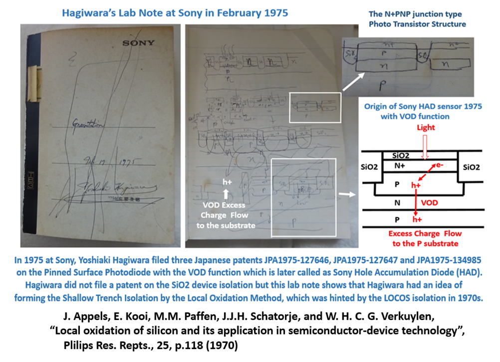
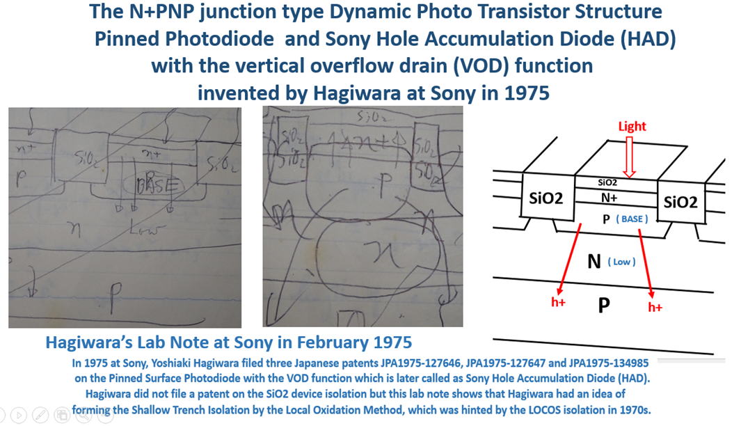
This Pinned Photodiode is based on the PNP dynamic photo transistor structure
that Hagiwara proposed in 1975 in his three original Japanese Patent ,
1975-134985, 1975-127646, and 1975-127647.
This fact is not widely known in the international world.
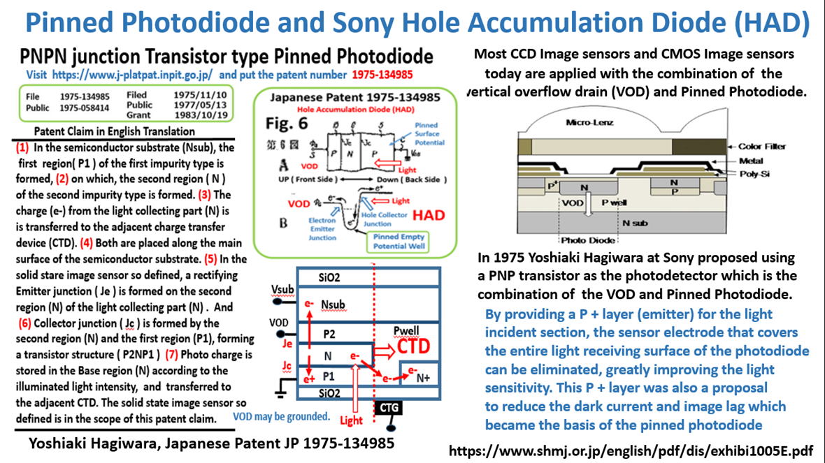
The PNP dynamic photo transistor structure was published
for the first time in the world in Hagiwara SSDM1978 paper.
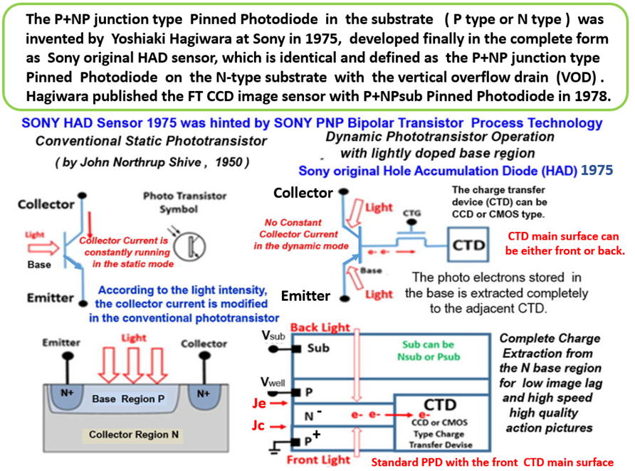
Hole Accumulation Diode is a PNPN junction type Dynamic Photo Transistor
which is Hagiwara 1975 invention of a Pinned Photodiode (PPD) with the
vertical overflow drain (VOD) structure.
Please note that the static photo transistor was invented already in 1950s.
http://www.aiplab.com/image19.jpg
As you know, the dynamic ITIC DRAM changed the world.
The PNPN junction dynamic photo transistor that Hagiwara proposed
in the Japanese Paptent 1975-134985 became now the basic of
the NEC 1982 Buried Photodiode, the Kodak 1984 Pinned Photodiode
and the Sony 1987 Hole Accumulation diode (HAD).
https://www.shmj.or.jp/english/pdf/dis/exhibi1005E.pdf
++++++++++++++++++++++++++++++++++++++++++++++++++++++++++++++++++++
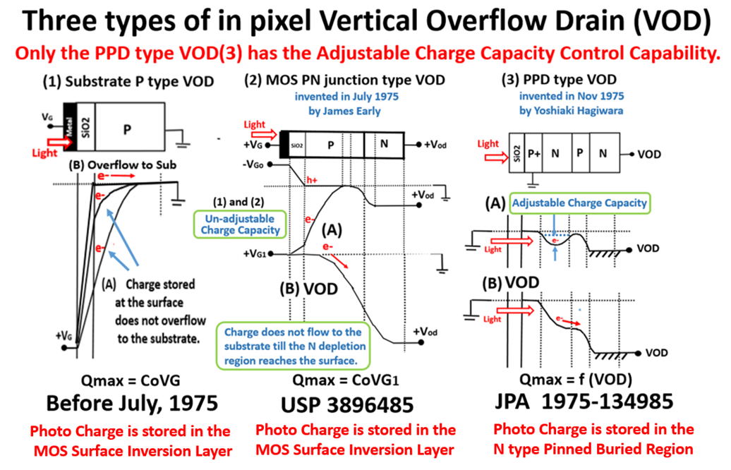
Pinned Photodiode must have the heavily doped channel stops nearby
and also completely buried signal charge collection and storage N region.
++++++++++++++++++++++++++++++++++++++++++++++++++++++++++++++++++++
In 1975, Sony proposed the Pinned surface PNP and PNPN junction type
dynamic phototransistor with the in pixel vertical overflow drain (VOD)
function for light detecting devices.
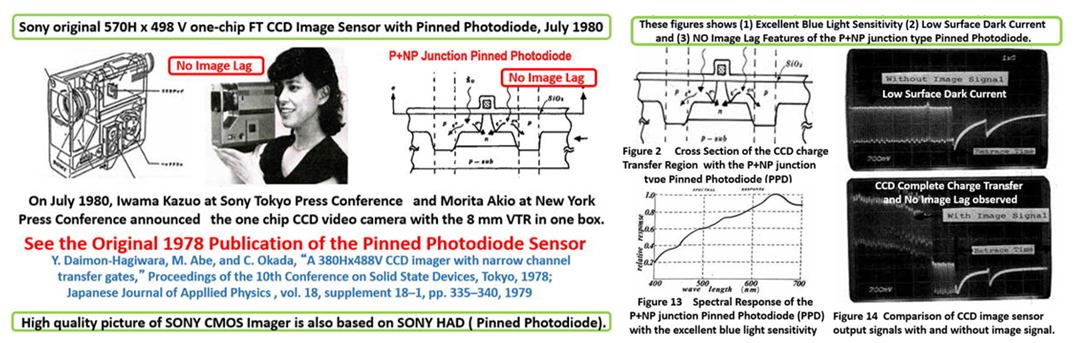
In 1978, Sony introduced one chip FT CCD image sensor with the Pinned
surface PNP junction type dynamic phototransistor which then became
the primary photodetector for CCD image sensors.
In 1984 Kodak called the Sony original Pinned surface PNP junction type
dynamic phototransistor simply as Pinnned Photodiode.
In 1987, Sony introduced a 2/3 inch, 380,000-pixel CCD image sensor
(ICX022) with the Pinned surface NPNP junction type dynamic Photo
Thryristor with VOD function which Sony then called simply as Hole
Accumulation Diode (HAD).
In the 1990s, the era of passport size video cameras demands compact
CCD image sensors with large numbers of pixels (1/2 inch or smaller
with 400,000 pixels or more).
In 1995, Kodak adopted Pinned Photodiode for CMOS image sensors.
Pinned Photodiodes, since invention by Sony in 1975, are still
the primary photodetector for CCD and CMOS image sensors now.
+++++++++++++++++++++++++++++++++++++++++++++++++++++++++
Return to AIPS HomePage