
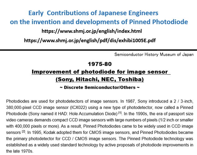
******************************************
What is Pinned Photodiode ?
******************************************
*********************************************************
Return to Top Page
*********************************************************
hagiwara-yoshiaki@aiplab.com ( http://www.aiplab.com/ )
hagiwara@ssis.or.jp ( http://www.ssis.or.jp/en/index.html )
*********************************************************
https://www.shmj.or.jp/english/index.html
https://www.shmj.or.jp/english/pdf/dis/exhibi1005E.pdf
*************************************************
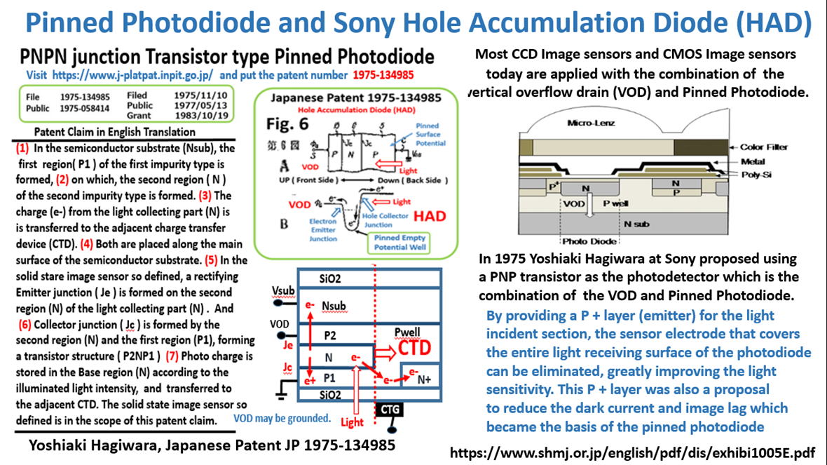
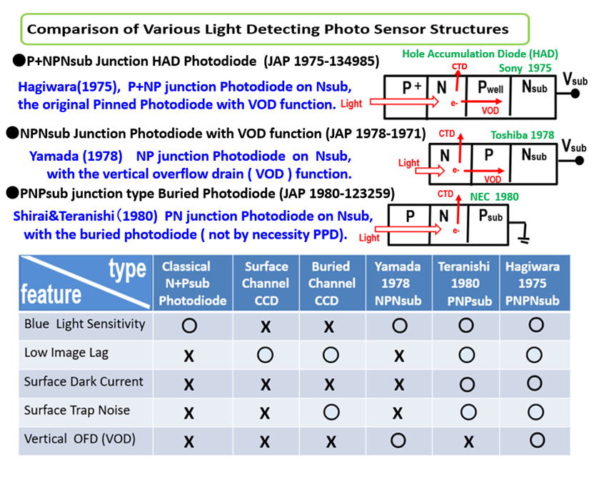
The original three basic Japapese Patents by Yoshiaki Hagiwara in 1975
on the Pinned Photodiode and Sony Hole Accumutaion Diode (HAD).
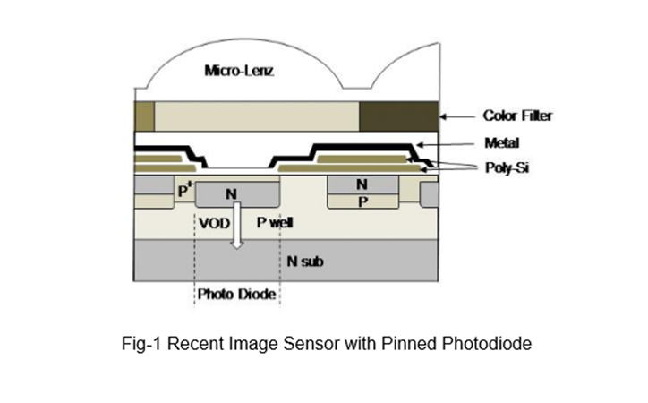
(1) N+NP+NP junction Pinned Photodiode with back light illumination scheme
with MOS Buffer Memory Capacitor for Global Shutter Function
Japanese Patent 1975-127646
(2) N+NP+N junction Pinned Photodiode with back light illumination scheme
with MOS Buffer Memory Capacitor for Global Shutter Function
Japanese Patent 1975-127647
(3) P+NP junction Pinned Photodiode formed on N substrate wafer
which is the Pinned Photodiode with the vertical overflow drain (VOD) function.
This is the original basic patent on the Sony Hole Accuulation Diode (HAD).
Japanese Patent 1975-134985
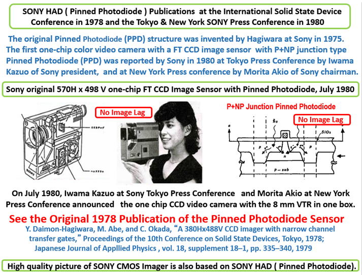
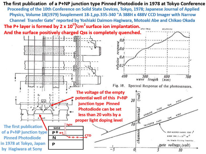
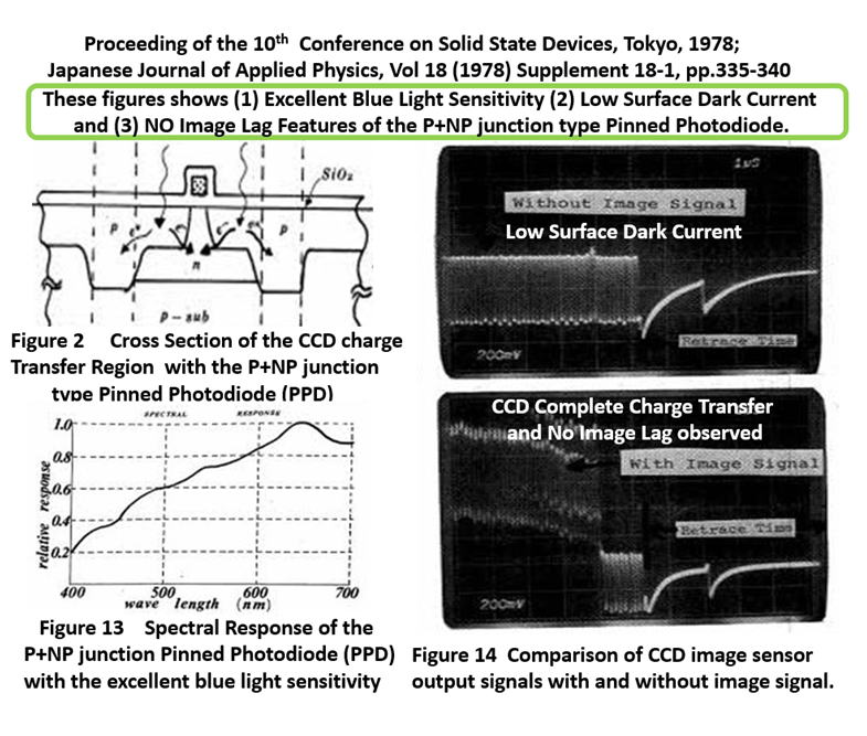
(4) Original P+NP junction Pinned Photodiode 1978 Paper
"A 380H x 488V CCD Imager with Narrow Channel Transfer Gates"
Proceeding of the 10th Conference on Solid State Devices, Tokyo 1978;
Japanese Journal of Applied Physics, Vol 18 (1979) Supplement 18-1,pp.335-340
*************************************************
(4) NP junction photodiode formed on N substrate wafer.
Japanese Patent 1978-1971
(5) PN junction Photodiode formed on P substrate wafer
Japanese Patent 1980-123259
*************************************************
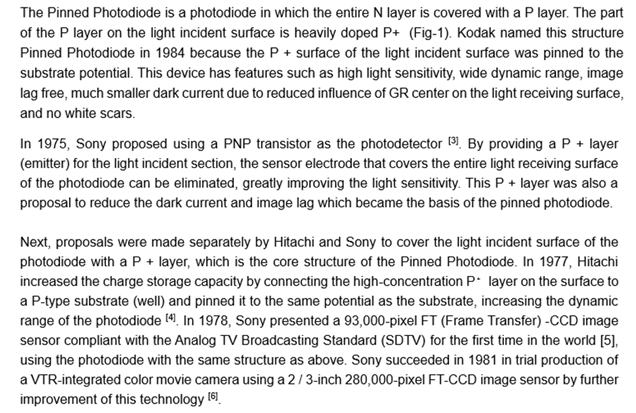
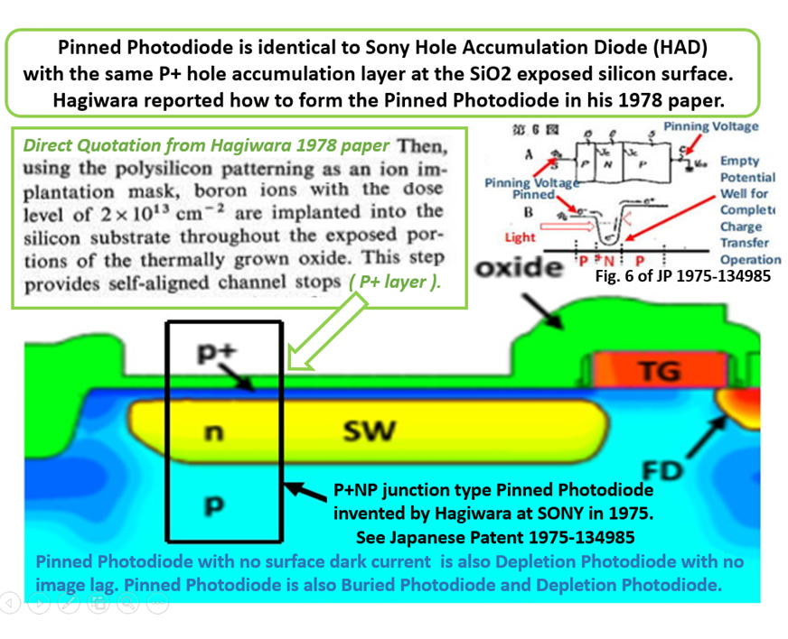
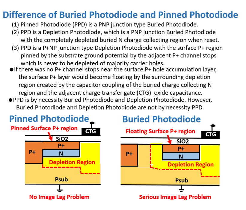
Pinned Photodiode is by definition the PNP junction type photodiode
with the pinned surface P region, which has three important features.
They are (1) Excellent Blue Light Sensitivity (2) Low Surface Dark
Current and (3) No image lag problem with the complete charge
transfer mode with the empty potential well at the reset time.
Sony Hole Accumulation is by definition the PNPN junction type
photodiode which is actually the PNP junction type Pinned Photodiode
with the built-in vertical overflow drain (VOD) function in each pixel.
*************************
No Image Lag Feature
*************************
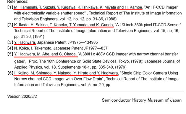
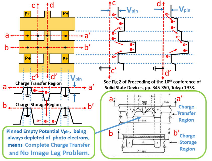
No Image Lag Feature was explained in Hagiwara 1975 Patents.

Hagiwara at SONY reported in his SSDM 1978 paper the P+NP juntion type
Pinned Phtoodiode (PPD) where the P+ and P layers have the same potential.
SONY used this PPD in Frame Trandfer CCD image sensor in SSDM1978 paper.
The pinned surface potential also defines the pinned empty potential well
of the buried N diffuison region, which can stay empty always in case of
the frame transfer CCD image sensor cases.
SONY reported the P+NP juntion type Pinned Phtoodiode (PPD)
where the surface P+ is pinned to the adjacent channel stops.
SONY used this highly blue light sensitive Pinned Phtoodiode (PPD)
in Frame Trandfer CCD image sensor in SSDM1978 paper.
*************************
Blue Light Sensitivity
*************************
The most important feature of the Pinned Photodiode
is the excellent short wave blue light sensitivity.
******************************
Low Surface Dark Current
******************************
Another important feature of the Pinned Photodiode
is the very low surface dark current feature.
The Pinned Photodiode was hinted by the original Sony SiO2 exposed Photo
Sensor.
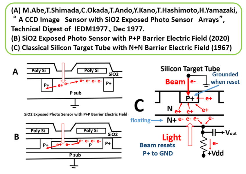
Sony developed the P+NPwellNsub structure and used it in interline transfer
CCD
and named this PPD + VOD structure the SONY Hole Accumulation Diode (HAD).
PPD has the pinned surface potentail as well as the pinned empty potential well
of the complete charge transfer operation resulting the no image lag picture quality
for fast action pictures. Hagiwara invented Buried Photodiode, Pinned Photodiode
and SONY Hole Accumulation Diode (HAD).
The evidence are give in Japanese 1975-127647 and 1975-134985 patents and
Hagiwara SSDM1978 paper on the P+NP junction type Pinned Photodidoe (PPD)
used in Frame Trandfer CCD image sensor.
Hagiwara recently published in the IEEE 3DIC2019 conference held in Sendai, Japan,
also a paper on the three dimensional back light illuminated Pinned Phtotodiode.

The 1975 Pinned Photodiode invention was hinted by Sony Original Bipolar
Technology.
SONY Image Sensors were developped by the experienced Bipolar Process Engineers,
educated and guided by Kawana-san and Kato-san, who are the pioneering
SONY
Bipolar Process engineers in 1950s and 1960s. Later, Iwama-san ( SONY President
)
appointed Kawana-san and Kato-san as the top management leaders of SONY
CCD
Image Sesnor Process Developments. Hagiwara later in 1975 joined SONY as the chief
design engineer of the CCD image sensors, and worked for Kawana-san and
Kato-san.
![]()
SONY HAD was hinted by the SONY Bipolar Process Technology developed
by Kawana san and Kato-san. The PNP junction transistors were known to
be built on the N substrate to form the PNPNsub junction thyristor structure.
However, the thyristor punch thru operation mode was a headache for reliabilty
process and device engineers. Hagiwara in 1975 made use of this punch thru
effect as the vertical overflow drain (VOD) in Japanese 1975-134985 patent.
*********************************************************
Hagiwara Publication List
*********************************************************
hagiwara-yoshiaki@aiplab.com ( http://www.aiplab.com/ )
hagiwara@ssis.or.jp ( http://www.ssis.or.jp/en/index.html )
*********************************************************
Return to Top Page
*********************************************************