*********************************************************
hagiwara-yoshiaki@aiplab.com ( http://www.aiplab.com/ )
hagiwara@ssis.or.jp ( http://www.ssis.or.jp/en/index.html )
*********************************************************
return to the TOP Page
*********************************************************
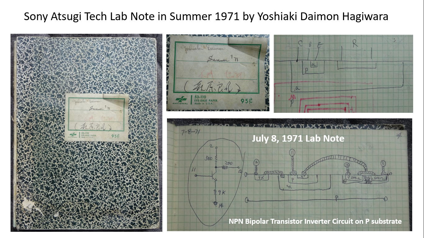
One invention was perfected by the ideas and efforts of
many diligent engineers and scientists. I worked for
image sensors in Sony only from 1975 till 1980. Then
I focused my attention to develop the digital camera
system LSI chips which was my life work in Sony.
I had a very wonderful time in Sony with many friends
working together with me, and still enjoying working for
future vision system chips for AI IoT Robotics world.
*********************************************************
https://electronics.stackexchange.com/questions/83018/difference-between-buried-photodiode-and-pinned-photodiode
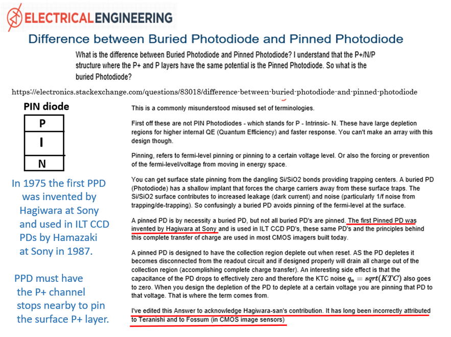
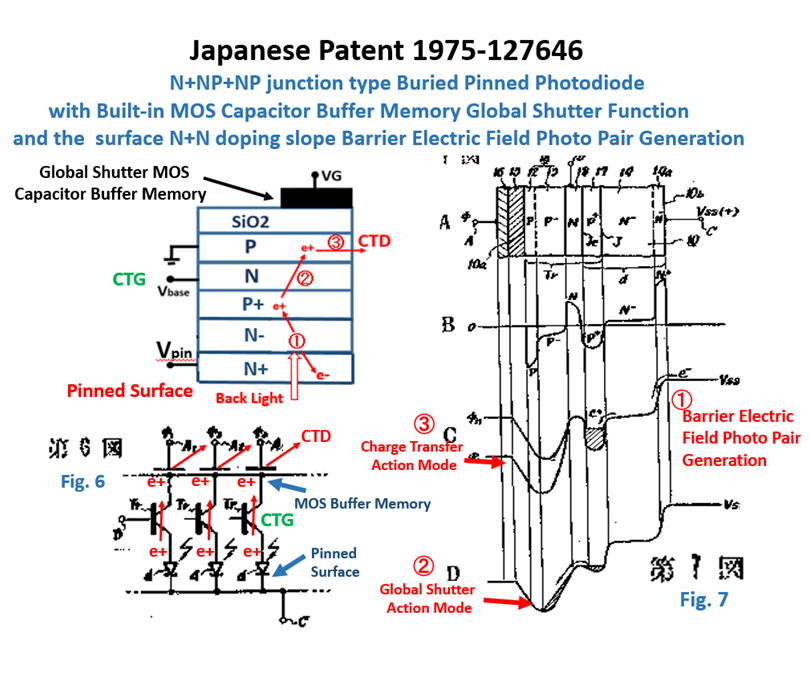
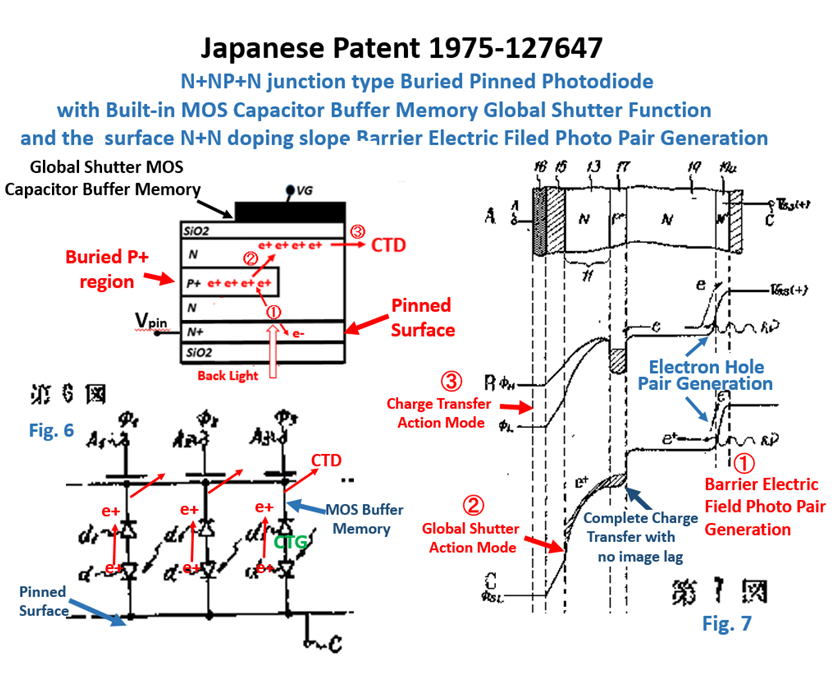
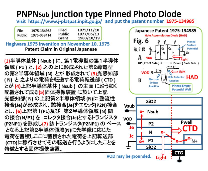
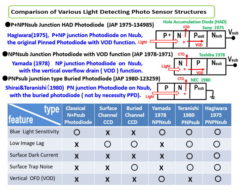
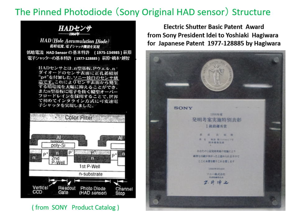
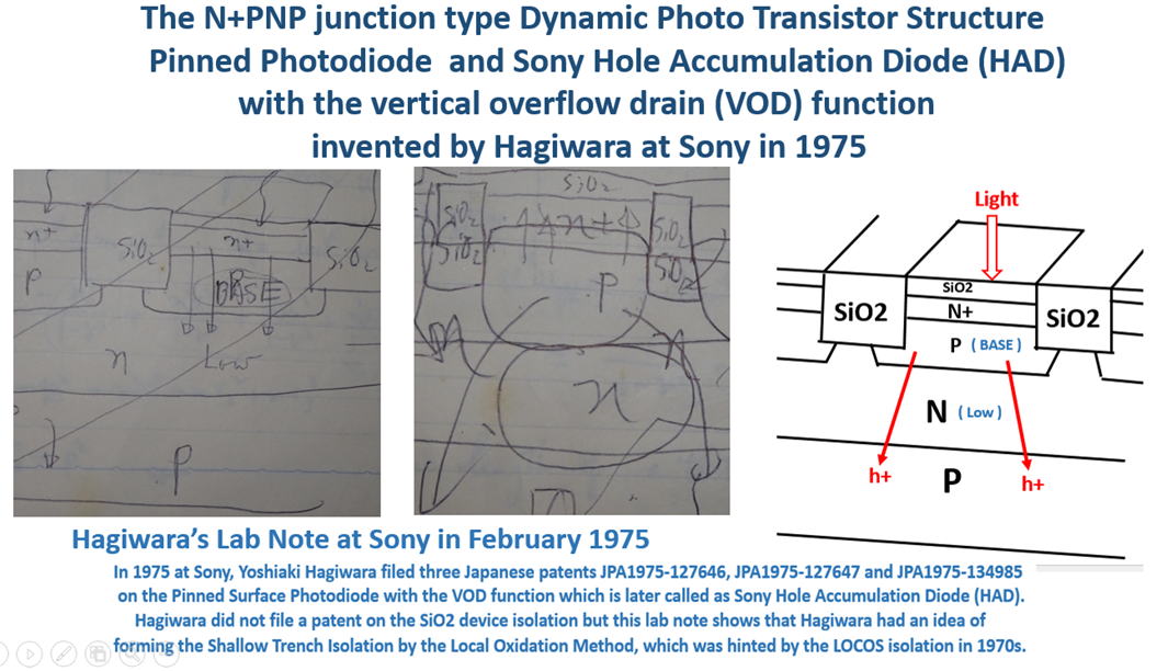
I have the basic patent 1975-128885 on the electrical shutter function
on the dynamic PNPN junction type photodiode which, as you know, later
became the basis of the PNP jucntion NEC and Kodak Pinned Photodiode
and the NPNP jucntion Sony Hole Accumulation Diode (HAD).
http://www.aiplab.com/Sony_patent_Award_on_Electric_Shutter_HAD.jpg
I was awarded internally in Sony by Idei san, Sony President and CEO,
for the invention of the Sony Hole Accumulation Diode with the vertical
overflow drain (VOD) function scheme for the 1977-128885 Japanese Patent.
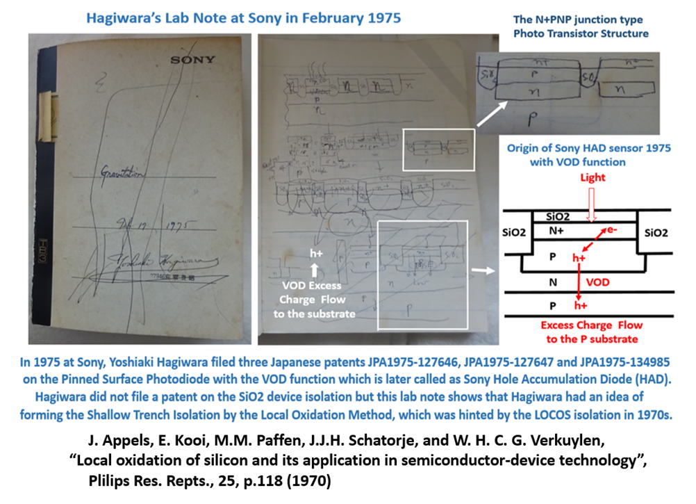
These old patents of mine ( JP1975-124676, JP1975-127647, JP1975-134985
and JP1977-128885 ) were all written in Japanese and were never disclosed
to the international world in details and causing many misunderstandings.
At that time in 1970s, we never thought the importance of patent files.
We were very busy to build a good image sensor for our customer market.
It was all my fault that I never explained these important ideas of mine
in details in the international English Journal and publications.
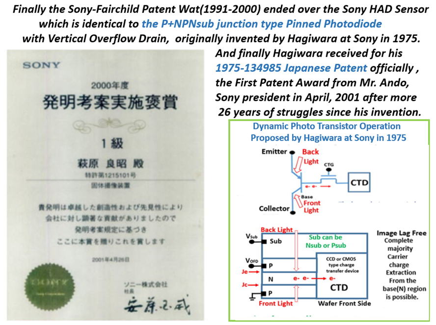
But I strongly believe that I invented the dynamic photo transistor
with the excellent light sensitivity, the extremely low surface dark current,
the extreme low image lag, the in pixel overflow drain(VOD), and the in pixel
MOS buffer memory for the Global shutter operation which is essential
for modern CMOS image sensors. In 1975, I also had the idea of the back
light illumination scheme for the dynamic photo transistor which is very
promising for building the three dimensional (3D) multi stacked integration
for a high performance real time robot vision system.
http://www.aiplab.com/P2019_3DIC2019Paper_on_3D_Pinned_Photodiode.pdf
http://www.aiplab.com/P2020_EDTM2020_PaperID_3C4_by_Hagiwara.pdf
I believe my inventions served as the initiator to accelerate Sony, Kodak and
other companies to build the digital camera and change the world from the
analog life style of film media to the new digital life style for AI IoT Robotics
for the future.

*********************************************************
The following WEB site explains very well what is Pinned Photodiode.
https://en.wikipedia.org/wiki/Photodiode#Pinned_photodiode
This Pinned Photodiode is based on the PNP dynamic photo transistor structure
that Hagiwara proposed in 1975 in his Japanese Patent 1975-134985, 1975-127646,
and 1975-127647.
This fact is not widely known in the international world.
The PNP dynamic photo transistor structure was published
for the first time in the world in my SSDNM1978 paper.
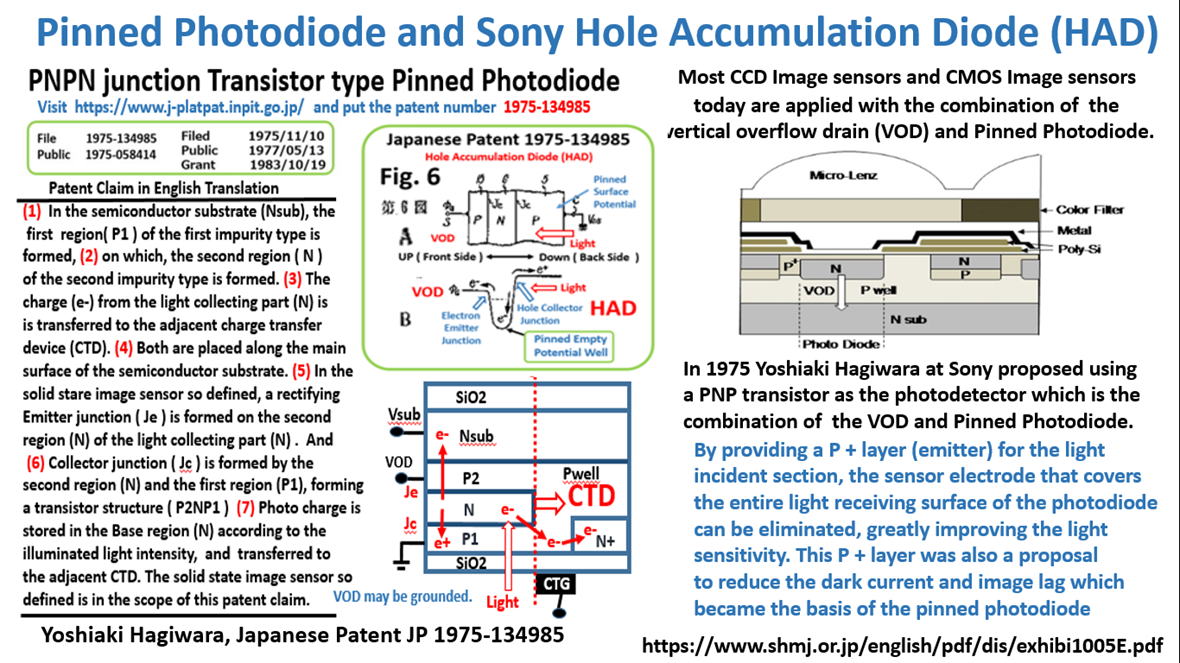
Hole Accumulation Diode is a PNPN junction type Dynamic Photo Transistor
which is Hagiwara 1975 invention of a Pinned Photodiode (PPD) with the
vertical overflow drain (VOD) structure.
Please note that the static photo transistor was invented already in 1950s.
http://www.aiplab.com/image19.jpg
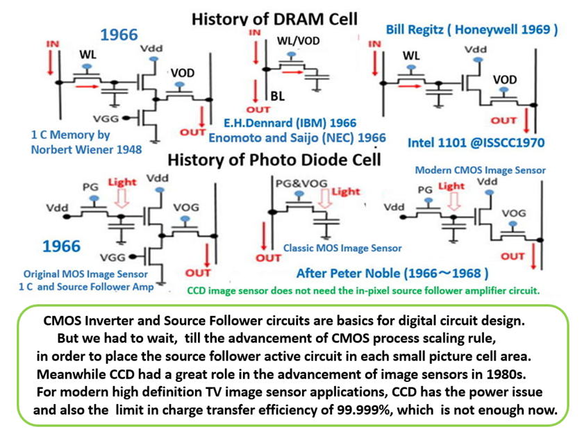
But as you know, the dynamic ITIC DRAM changed the world.
The dynamic photo transistor I proposed in JPA 1975-134985
became now the basic of the NEC 1982 Buried Photodiode,
the Kodak 1984 Pinned Photodiode and the Sony 1987 HAD.
https://www.shmj.or.jp/english/pdf/dis/exhibi1005E.pdf
http://www.aiplab.com/image17.jpg
http://www.aiplab.com/image7.jpg
http://www.aiplab.com/NPNP_junction_Pinned_Photodiode_in_1975_by_Hagiwara.jpg
https://en.wikipedia.org/wiki/Photodiode#Pinned_photodiode
This Pinned Photodiode is based on the PNP dynamic photo transistor structure
that Hagiwara proposed in 1975 in his Japanese Patent 1975-134985, 1975-127646,
and 1975-127647.
This fact is not widely known in the international world.
The PNP dynamic photo transistor structure was published
for the first time in the world in my SSDNM1978 paper.
Hole Accumulation Diode is a PNPN junction type Dynamic Photo Transistor
which is Hagiwara 1975 invention of a Pinned Photodiode (PPD) with the
vertical overflow drain (VOD) structure.
Please note that the static photo transistor was invented already in 1950s.
http://www.aiplab.com/image19.jpg
But as you know, the dynamic ITIC DRAM changed the world.
The dynamic photo transistor I proposed in JPA 1975-134985
became now the basic of the NEC 1982 Buried Photodiode,
the Kodak 1984 Pinned Photodiode and the Sony 1987 HAD.
https://www.shmj.or.jp/english/pdf/dis/exhibi1005E.pdf
http://www.aiplab.com/image17.jpg
http://www.aiplab.com/image7.jpg
http://www.aiplab.com/NPNP_junction_Pinned_Photodiode_in_1975_by_Hagiwara.jpg
![]()

*********************************************************
https://www.shmj.or.jp/english/index.html
https://www.shmj.or.jp/english/pdf/dis/exhibi1005E.pdf
PS3_Cell_Proceesor_Sony_Team_Award
https://ieeexplore.ieee.org/document/4681786
Invited Talk at ESSCIRC2008
ISSCC2003_Executive_Committee_Contribution_Award

++++++++++++++++++++++++++++++++++++++++++++++++
My achievement can be summarize as
the contribution to the AI IoT Robotics world
thru the invention and the development efforts
of all solid state intelligent electric eye and
the technical contribution in the SONY SOI cell
processor development.
++++++++++++++++++++++++++++++++++++++++++++++++
the following documents may explain my life work.
https://www.imagesensors.org/Past%20Workshops/1979%20CCD79/03-1%20Hagiwara.pdf
http://www.aiplab.com/P1989_SONY_4MSRAM_1989.pdf
http://www.aiplab.com/P2001_ESSCIRC2001.pdf
http://www.aiplab.com/P2008_ESSCIRC2008Hagiwara.pdf
http://www.aiplab.com/P2013_ISSCC2013PanelTalk.pdf
http://www.aiplab.com/P2019_3DIC2019Paper_on_3D_Pinned_Photodiode.pdf
http://www.aiplab.com/P2020_EDTM2020_PaperID_3C4_by_Hagiwara.pdf
The followings are images of my life work
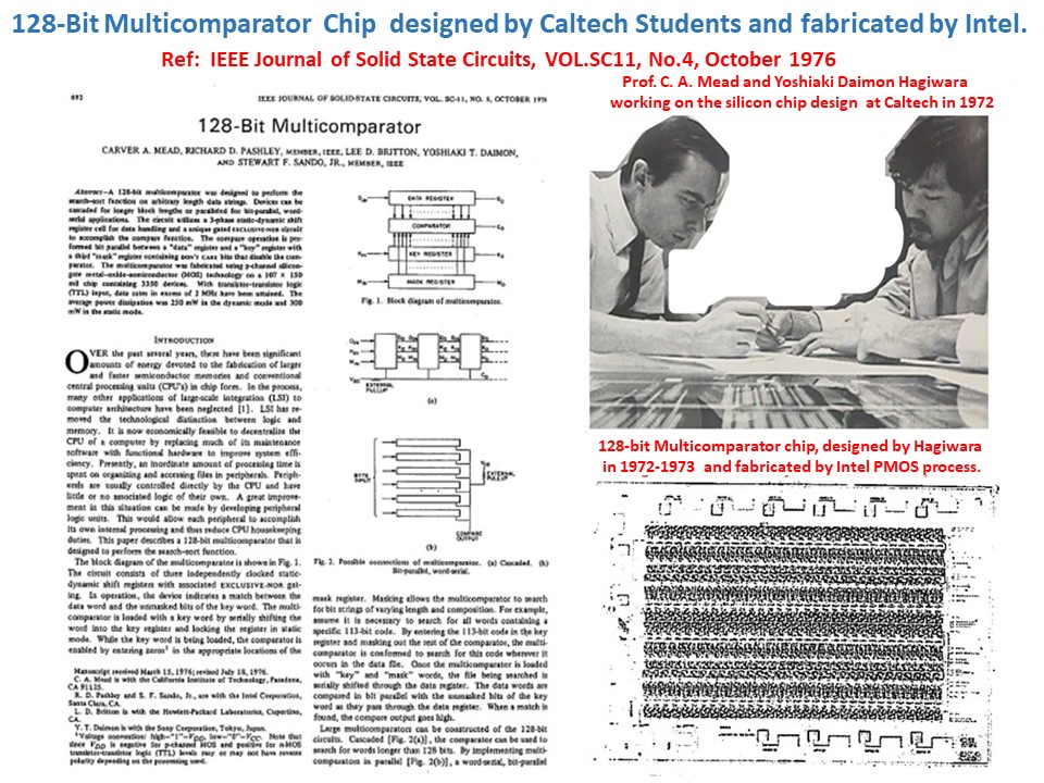
http://www.aiplab.com/P1976_128_bit_Comparator.jpg
http://www.aiplab.com/image25.jpg
http://www.aiplab.com/image14.jpg
http://www.aiplab.com/HanoiTower.jpg
http://www.aiplab.com/CoffeeCup.jpg
http://www.aiplab.com/image.jpg
++++++++++++++++++++++++++++++++++++++++++++++++
My achievement can be summarize as
the contribution to the AI IoT Robotics world
thru the invention and the development efforts
of all solid state intelligent electric eye and
the technical contribution in the SONY SOI cell
processor development.
++++++++++++++++++++++++++++++++++++++++++++++++
******************************
My Work Summary
******************************
I was teaching graduate and undergraduate students at Sojo university
as a full professor of the information science department since 2009
till 2017. During the period I taught the various courses such as
Engineering Mathematics, Numerical Computational Method,
Semiconductor Device Physics, Digital Circuit and System Design
and Artificial Intelligent Robotics.
I wrote a book entitled as “The world of Digital Circuits” for
the Intelligent Partner System (AIPS) applications in 2016 which
summarizes the most of the scopes of my class teaching materials
focused to the physics of semiconductor and LSI chip designs.
My most important contribution to the world is that my inventions
and my development efforts helped and accelerated the world to
change from the analog to the digital world by replacing the film
and the mechanical shutter technologies by the all solid semiconductor
silicon chips in the field of the intelligent image sensor technology.
Specifically, my 1975 invention of three layer device of pnp dynamic
photo transistor structure, when the two layer photodiode of pn structure
was common at that time, was very unique and is a new dimensional
device for future 3DIC multi-chip integration for artificial intelligent
partner systems with a great deal of freedom for improving image
sensor performances, including super light sensitivity, the most
important characteristics of the image sensor device now used all
over the world.
This is the base of today’s photodiode called PPD or Pinned Photodiode,
which is widely used for various applications including smartphones,
robotics, and self-driving cars to name a few. Sony commercialized
image sensor devices based on his invention, with the trade name
of HAD (Hole Accumulation Diode) sensor, and has become a leading
manufacturer of digital cameras which replaced film cameras completely
in the world.
My 1975 inventions of the back light illumination mode pnp dynamic
photo transistor with in-pixel buffer memory MOS buffer memory
in the global shutter operation mode, is now very essential for
the modern CMOS image sensor applications.
Image sensors, now used for taking fast action pictures, are completely
free from mechanical parts because of my 1975 invention of the electrical
shutter operational four layer device of pnpn dynamic photo thyristor
which has a vertical overflow drain (VOD) structure.
I served many years as an operational committee member, the ISSCC Asian
Program committee chair and the international program chair of IEEE Solid
State Circuit Society sponsored ISSCC conferences in series.
I was also invited as a special guest speaker in CCD1979, ESSCIRC2001,
ESSCIRC2008 and ISSCC2013 for his contributions to the solid state circuits
technology needed to change the image sensor world from the analog
to digital one.
I also served many years as an operational committee member and the conference
chair in the IEEE Electron Device Society sponsored ICMTS conferences in series.
I served as a technical committee member for many years in the international
standardization committee (IEC) and served as the IEC TC47 technical committee
chair in 1992 in the field of the digital memory chips standardization activities in IEC.
I am a distinguished alumni of California Institute of Technology and IEEE Life fellow.
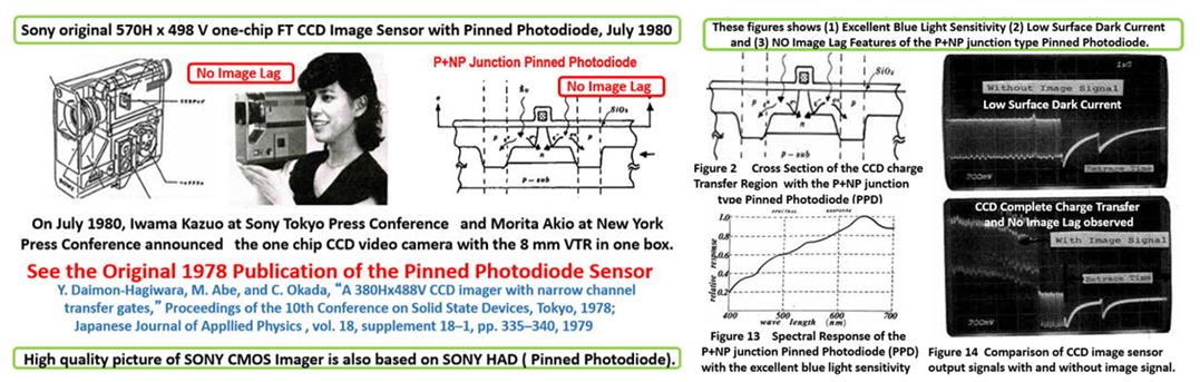
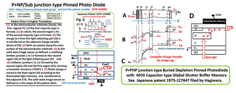
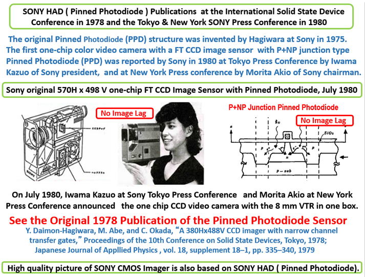
The first Image Lag free FT CCD image sensor
with the PNP junction type Pinned Photodiode was
reported at SSDM1978 by Yoshiaki Hagiwara at Sony.
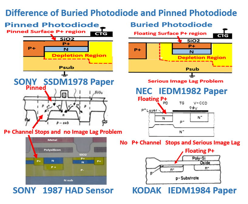
The first Image Lag free ILT CCD image sensor
with the PNPN junction type Pinned Photodiode
and the VOD electrical shutter function was
reported in the Journal of Nikkei Microdevices,
October 1987 Issue by Masao Hamazaki at Sony.
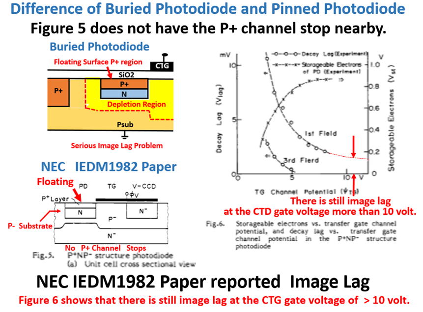
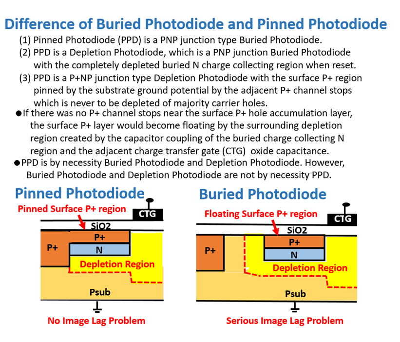
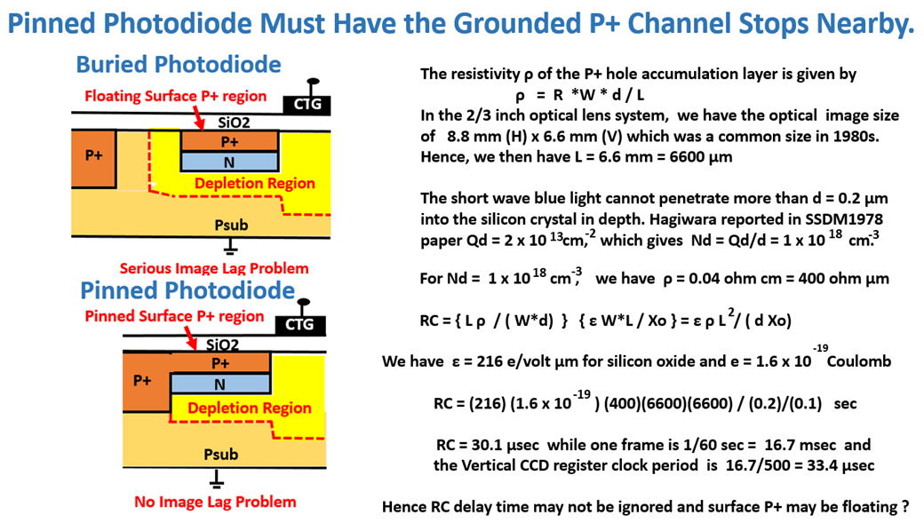
NEC IEDM1982 paper reported the image lag data.
The image lag is due to the RC delay of
the floating surface P+ layer ?
The details are explained below :
http://www.aiplab.com/Pinned_Photodiode_must_have_a_heavy_doped_Channel_Stops.pdf
<<<<<<<<<<<<<<<<<<<<<<<<<<<<<<<<<<<<<<<<<<<<<<<<<<
Summary of Achievements .
<<<<<<<<<<<<<<<<<<<<<<<<<<<<<<<<<<<<<<<<<<<<<<<<<<
Hagiwara proposed three layer device of pnp dynamic photo
transistor structure in 1975, when the two layer photodiode of pn
structure was common. This device is very unique and a new
dimensional device with a great deal of freedom for improving the
performance of image sensors used all over the world, including
the super light sensitivity feature, the most important characteristics
of the image sensor device. This is the base of today’s photodiode
called PPD or Pinned Photodiode, which is widely used for various
applications including smartphones, robotics, and self-driving cars
to name a few. Sony commercialized image sensor devices based
on his invention, with the trade name of HAD Sensor (HAD for Hole
Accumulation Diode), and has become a leading manufacturer of
image sensors in the world.
>>>>>>>>>>>>>>>>>>>>>>>>>>>>>>>>>>>>>>>>>>>>>>>>>>>
Please evaluate and judge my early works at SONY.
Related documents are uploaded from the following sites.
https://www.shmj.or.jp/english/pdf/dis/exhibi1005E.pdf
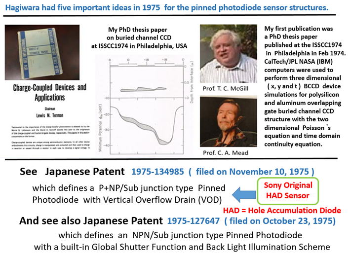
(1) My basic 1975 Japanese Patents of Pinned Photodiode
Japanese Patent 1975-127646 on N+NP+NP junction Pinned Photodiode
http://www.aiplab.com/JP1975-127646_A.jpg
http://www.aiplab.com/JP1975-127646.pdf
Japanese Patent 1975-127647 on N+NP+N junction Pinned Photodiode
http://www.aiplab.com/JP1975-127647_A.jpg
http://www.aiplab.com/JP1975-127647.pdf
Japanese Patent 1975-124985 on P+NPNsub junction Pinned Photodiode
http://www.aiplab.com/image7.jpg
http://www.aiplab.com/JP1975-134985.pdf
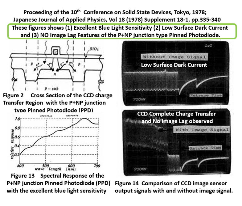
(2) My SSDM1978 paper on PNP junction Pinned Photodiode
http://www.aiplab.com/SSDM1978_A_Pinned_Photodiode.jpg
"A 380H x 488V CCD Imager with Narrow Channel Transfer Gates"
Proceeding of the 10th Conference on Solid State Devices, Tokyo 1978;
Japanese Journal of Applied Physics, Vol 18 (1979) Supplement 18-1,pp.335-340
Japanese Patent 1975-127647 on N+NP+N junction Pinned Photodiode
http://www.aiplab.com/P1978_Pinned_Photodiode_1978_Paper_by_Hagiwara.pdf
(3) My 3DIC2019 conference paper on 3D integration of Back Light illuminated Pinned Photodiode.
http://www.aiplab.com/image14.jpg
"Multichip CMOS Image Sensor Structure for Flash Image Acquisition"
IEEE International 3D Systems Integration Conference 2019 (3DIC2019)
Digest of Technical Papers, Sendai, Japan, Paper4017, October 2019
http://www.aiplab.com/P2019_3DIC2019Paper_on_3D_Pinned_Photodiode.pdf
(4) My EDTM2020 conference paper on P+PNP junction type Pined Photodiode.
"Simulation and Device Characterization of the P+PN+P Junction Type
Pinned Photodiode and Schottky Barrier Photodiode"
http://www.aiplab.com/P2020_EDTM2020_PaperID_3C4_by_Hagiwara.pdf
I really need your helps with the very good semiconductor device physics background
to evaluate my early works with the competent and fair judgment eyes.
I also spoke in the following conferences.
http://www.aiplab.com/P1979_CCD79_in_Edinbourgh_1979.pdf
http://www.aiplab.com/P2001_ESSCIRC2001.pdf
http://www.aiplab.com/P2008_ESSCIRC2008Hagiwara.pdf
http://www.aiplab.com/P2013_ISSCC2013PanelTalk.pdf
******************************
Hagiwara Important Publication & Patent Works
Japanese Patent 1975-127646 on N+NP+NP junction Pinned Photodiode
Japanese Patent 1975-127647 on N+NP+N junction Pinned Phtotodiode
Japanese Patent 1975-124985 on P+NPNsub junction Pinned Photodiode
(1) 1973 Paper
"The Influence of Interface States on Incomplete Charge Transfer
in Overlapping Gate Charge Coupled Devices",
IEEE Journal of Solid State Circuits, Vol. SC 8, No.2, April 1973
(2) 1974 Paper ( Hagiwara PhD student Paper )
"Charge Transfer of Buried Channel Charge Coupled Devices"
Proceeding of International Solid State Circuit Conference (ISSCC),
San Francisco, Februrary 1974.
(3) 1974 Paper
"Final Stage of the Charge Transfer Process in Charge Coupled Devices"
IEEE Transactions on Electrron Devices, VOl. ED-21, No.4, April 1974
(4) 1976 Paper
128-bit Comparator Chip
(5) 1977 Paper
"Two Phase CCD with Narrow Channel Transfer Regions"
Proceeding of the 9th Conference on Solid State Devices, Tokyo 1977;
Japanese Journal of Applied Physics, Vol 17 (1978) Supplement 17-1,pp.255-261
(6) 1978 Paper
"A 380H x 488V CCD Imager with Narrow Channel Transfer Gates"
Proceeding of the 10th Conference on Solid State Devices, Tokyo 1978;
Japanese Journal of Applied Physics, Vol 18 (1979) Supplement 18-1,pp.335-340
(7) 1979
Paper Invited Talk at CCD'79 at Edinburgh, Scotland UK
(8) 1989 Paper
Paper on the Fast Cache 4 Mega bit Cache SRAM at ISSCC1989
(9) 2001 Paper
Invited Talk at ESSCIRC2001
(10) 2008 Paper
Invited Talk at ESSCIRC2008
(11) 2013 Talk
ISSCC2013 Plenary Panel Talk
(12) 2019 Paper
3DIC2019 Conference at Sendai, Japan 2019
(13) EDTM2020 PaperID3C-4
"Simulation and Device Characterization of the P+PN+P Junction Type
Pinned Photodiode and Schottky Barrier Photodiode"
*******
Awards
*******
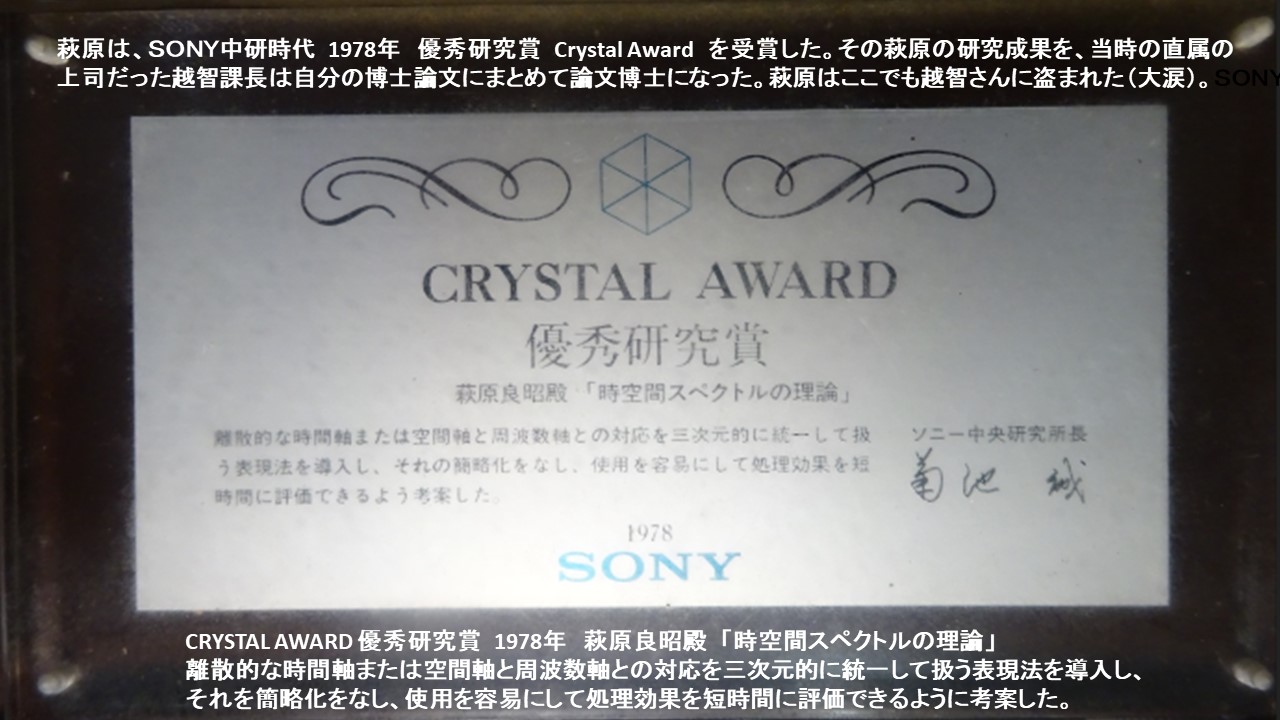
1978年 ソニー中央研究所 Crystal Award 優秀研究賞(個人)
1988年 ソニーCEO アワード (グループ受賞 )
( デジカメ用の高速 4M Cache SRAMの開発 )
1996年 ソニー発明考案実施特別表彰一級最優秀賞(個人受賞)
( 電子シャッター&ガンマ特性機能 )
2000年 ソニーSCプレジデントアワード(個人受賞 )
( SONY 対 Fairchild社の特許戦争への貢献 )
2000年 ソニー発明考案実施褒賞一級(個人受賞)
( SONY HAD = Pinned Photodiode + VOD )
2001年 IEEE Fellow
2002年 米国 カリフォルニア工科大学 Distinguished Alumni Award
2008年 IEEE ICMTS運営委員会 Service Award (功労表彰)
2013年 IEEE ISSCC運営委員会 Service Award (功労表彰)
2018年 IEEE Life Fellow
***********
Publications
***********


(27) EDTM2020_PaperID3C-4
"Simulation and Device Characterization of the P+PN+P Junction Type
Pinned Photodiode and Schottky Barrier Photodiode"
*********************************************************
*********************************************************
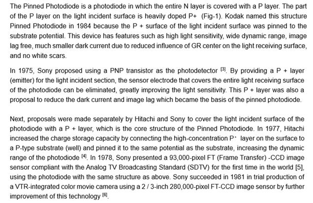
What is Pinned Photodiode ?
Study Special Relativity Theory
What is Abura Wake Zan ?
Study Korean for Your Enjoyment
Enjoy C-programming.
IEEE_EDS_Kansai_Chapter_IMFEDK2006_Hagiwara.pdf
DRAM_SRAM_Technology_and_Problems_1998_07_29_Hagiwara
Pinned_Photodiode_must_have_a_heavy_doped_Channel_Stops
++++++++++++++++++++++++++++++++++++++++++++++++++++++++++++++++++++
Pinned Photodiode must have the heavily doped channel stops nearby
and also completely buried signal charge collection and storage N region.
++++++++++++++++++++++++++++++++++++++++++++++++++++++++++++++++++++
In 1975, Sony proposed the Pinned surface PNP and PNPN junction type
dynamic phototransistor with the in pixel vertical overflow drain (VOD)
function for light detecting devices.
In 1978, Sony introduced one chip FT CCD image sensor with the Pinned
surface PNP junction type dynamic phototransistor which then became
the primary photodetector for CCD image sensors.
In 1984 Kodak called the Sony original Pinned surface PNP junction type
dynamic phototransistor simply as Pinnned Photodiode.
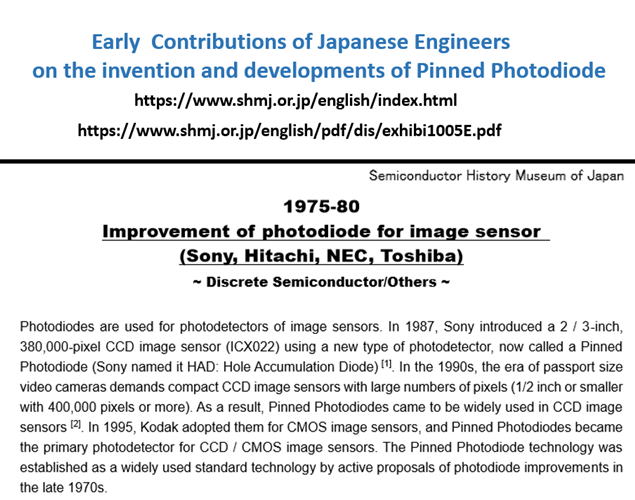
In 1987, Sony introduced a 2/3 inch, 380,000-pixel CCD image sensor
(ICX022) with the Pinned surface NPNP junction type dynamic Photo
Thryristor with VOD function which Sony then called simply as Hole
Accumulation Diode (HAD).
In the 1990s, the era of passport size video cameras demands compact
CCD image sensors with large numbers of pixels (1/2 inch or smaller
with 400,000 pixels or more).
In 1995, Kodak adopted Pinned Photodiode for CMOS image sensors.
Pinned Photodiodes, since invention by Sony in 1975, are still
the primary photodetector for CCD and CMOS image sensors now.
+++++++++++++++++++++++++++++++++++++++++++++++++++++++++
![]()
Slide2020_05_31
Slide2020_06_10
Slide2020_06_10a
Slide2020_06_11
Slide2020_06_19
Slide2020_06_24
*********************************************************
hagiwara-yoshiaki@aiplab.com ( http://www.aiplab.com/ )
hagiwara@ssis.or.jp ( http://www.ssis.or.jp/en/index.html )
*********************************************************
return to the TOP Page
*********************************************************