


***********************************************
******
豆知識 <-- 萩原良昭が知らなかった言葉です(苦笑)。
******
岳樺(ダケカンバ)
木犀(もくせい)
曼珠沙華(マンジュシャゲ)
欅(ケヤキ)
凭れる(もたれる)
繁(しげ)
諍(いさか)う
言争(いいあらがう)
ひぐらし
ユキノシタ(雪の下)の花言葉とは?
切岸(きりぎし)とは?
莪 とは ?
蓼莪之詩 (りくがのし) とは ?
梢(こずえ) とは?
*************************************
********************************************
AIPS Library
*******************************************
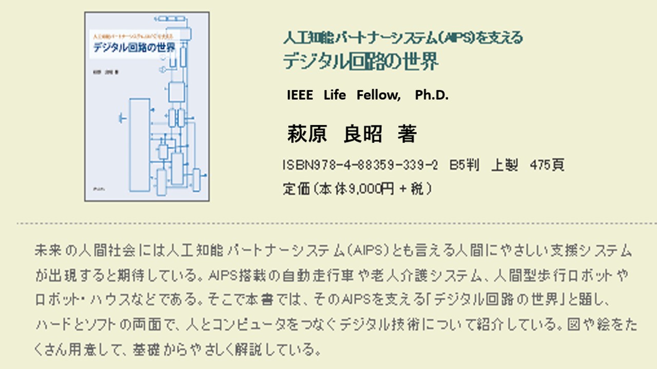
Yoshiaki Hagiwara wrote a book on
"the World of Artificial Intelligent Digital Circuits",
which is important and needed to built
the intelligent image sensor systems.
ISBM978-4-88359-339-2
Hard Cover, 460 page,
\ 9000 Japanese Yen + tax
If you are interestied in the book, Please visit
https://www.seizansha.co.jp/ISBN/ISBN978-4-88359-339-2.html
https://www.seizansha.co.jp/
*****************************
理解度アップの基本復習問題
*****************************
●Q01_受光素子とは何か?
●Q02_電荷転送装置とは?
●Q03_感度とは?
●Q04_CCD Image Sensor とは?
●Q05_CMOS Image Sensor とは?
●Q06_Correlated Double Sampling (CDS) とは?
●Q07_IN PIXEL 信号増幅回路 とは?
●Q08_Single接合型 Photodiode とは?
●Q09_Double 接合型 Photodiode とは?
●Q10_Buried Photodiode (BPD)とは?
●Q11_Pinned Photodiode (PPD)とは?
●Q12_Triple 接合型 Photodiode とは?
●Q13_Image Sensorに不可欠な重要特性とは?
●Q14_光感度とは?
●Q15_暗電流雑音とは?
●Q16_残像特性とは?
●Q17_強い入射光による光信号の調整機能とは?
●Q18_電子 shutter 機能とは?
●Q19_Rotary shutter 機能とは?
●Q20_Global shutter 機能とは?
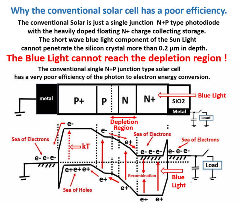
●Q21_太陽電池の動作原理とは?
●Q22_太陽電池の光電変換効率とは?
●Q23_Single 接合型太陽電池とは?
●Q24_Double 接合型太陽電池とは?
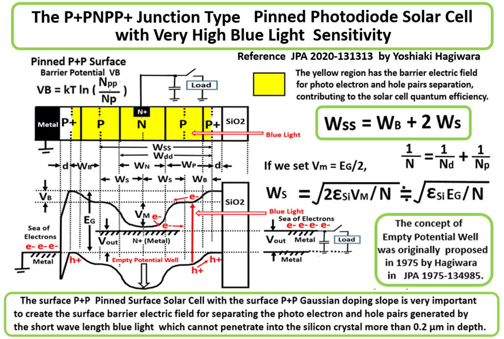
●Q25_Pinned Photodioce (PPD)型 太陽電池とは?
*****************************
++++++++++++++++++++++++++++++++++++++++++++++++++++++++++++++++++++++++++


++++++++++++++++++++++++++++++++++++++++++++++++++++++++++++++++
Gate Way to AIPS Library
++++++++++++++++++++++++++++++++++++++++++++++++++++++++++++++++
index_001_Enjoy_the_World_of_Hagiwara_Tomie_E_Tegami_Gallery.html
index_002_Enjoy_the_World_of_Hagiwara_Yoshiaki_Talks_and_Photo_Desk.html
index_003_Enjoy_the_World_of_Japanese_Short_Poem.html
index_004_Enjoy_the_World_of_Korean_Conversation.html
index_005_Enjoy_the_World_of_English_Conversation.html
index_006_Enjoy_the_World_of_Mathematics_Physics_and_Relativiry_Theory.html
index_007_Enjoy_the_World_of_Quantum_Mechanics_and_Semiconductor_Device_Physics.html
index_008_Enjoy_the_World_of_Artificial_Intelligent_Partner_System_AIPS_Digital_Circuits.html
index_009_Enjoy_the_World_of_Solid_State_Image_Sensors_and_PPD_Solar_Cells.html
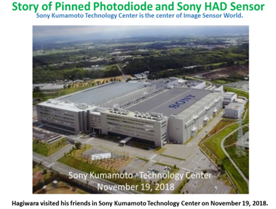
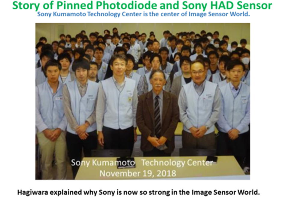
index_010_Hagiwara_is_the_true_inventor_of_Pinned_Photodiode_PPD_and_Sony_HAD.html
++++++++++++++++++++++++++++++++++++++++++++++++++++++++++++++++
+++++++++++++++++++++++++++++++++++++++++++++++++++++++++++++++++++++++++++++
Hagiwara_invented_PPD_and_Sony_HAD_in_1975.pdf
+++++++++++++++++++++++++++++++++++++++++++++++++++++++++++++++++++++++++++++
001_Hagiwara_invented_PPD_and_Sony_HAD_in_1975.pdf
002_Image_Sensor_Story_by_Hagiwara.pdf
003_Future_of_Image_Sensors_and_Solar_Cells.pdf
004_The_First_Pinned_Photodiode_was_invented_in_1975_by_Yoshiaki_Hagiwar_at_Sony.pdf
+++++++++++++++++++++++++++++++++++++++++++++++++++++++++++++++++++++++++++++
++++++++++++++++++++++++++++++++++++++++++++++++++++++++++++++++++++++++++
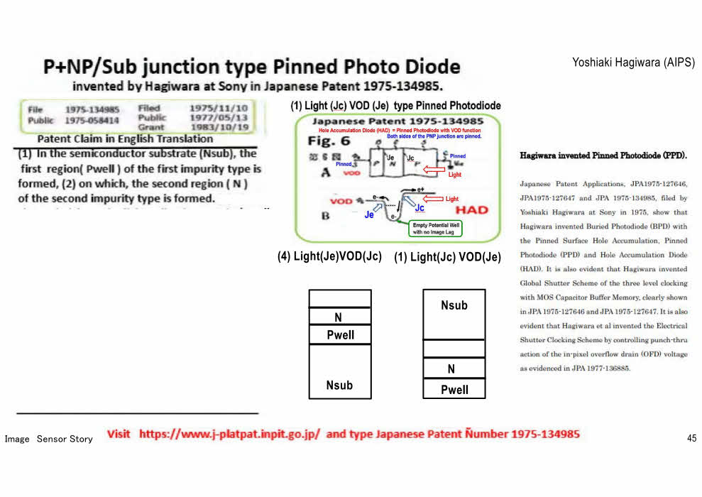
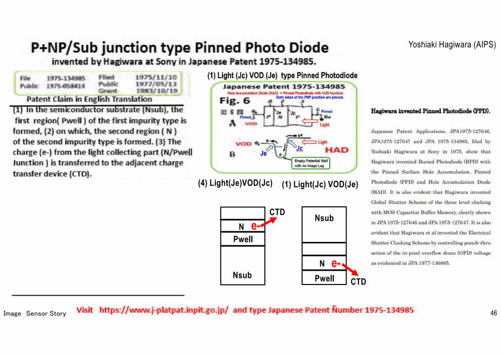
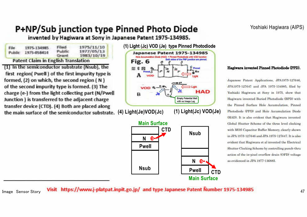
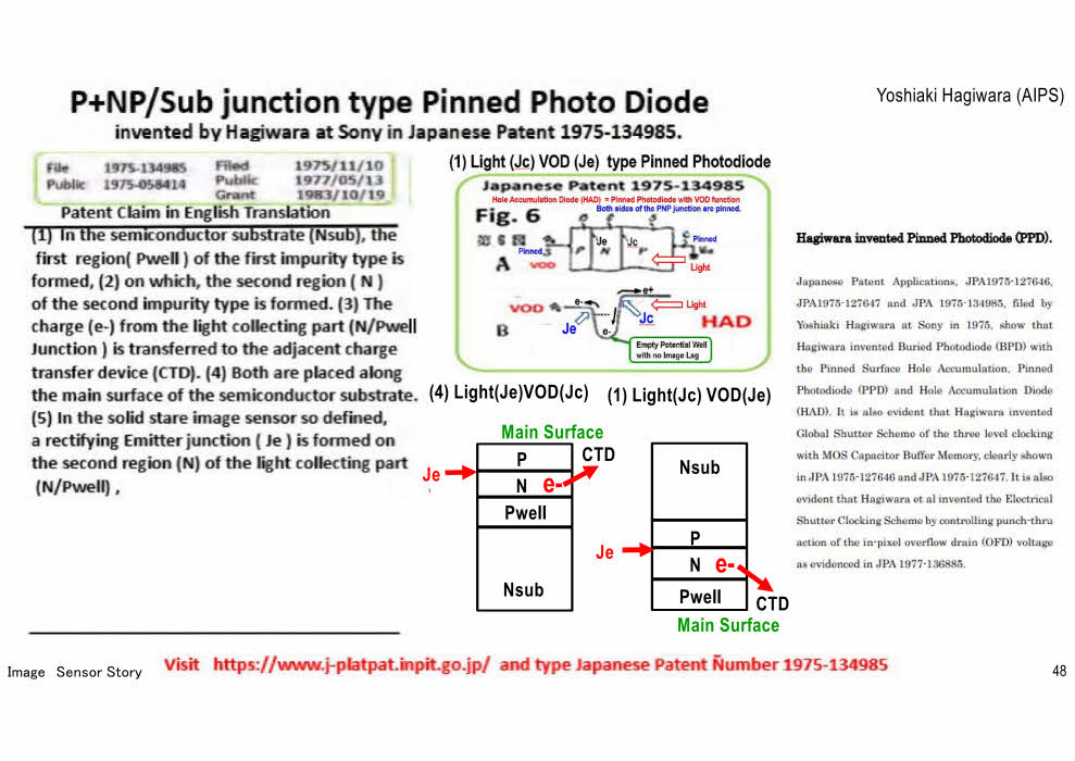
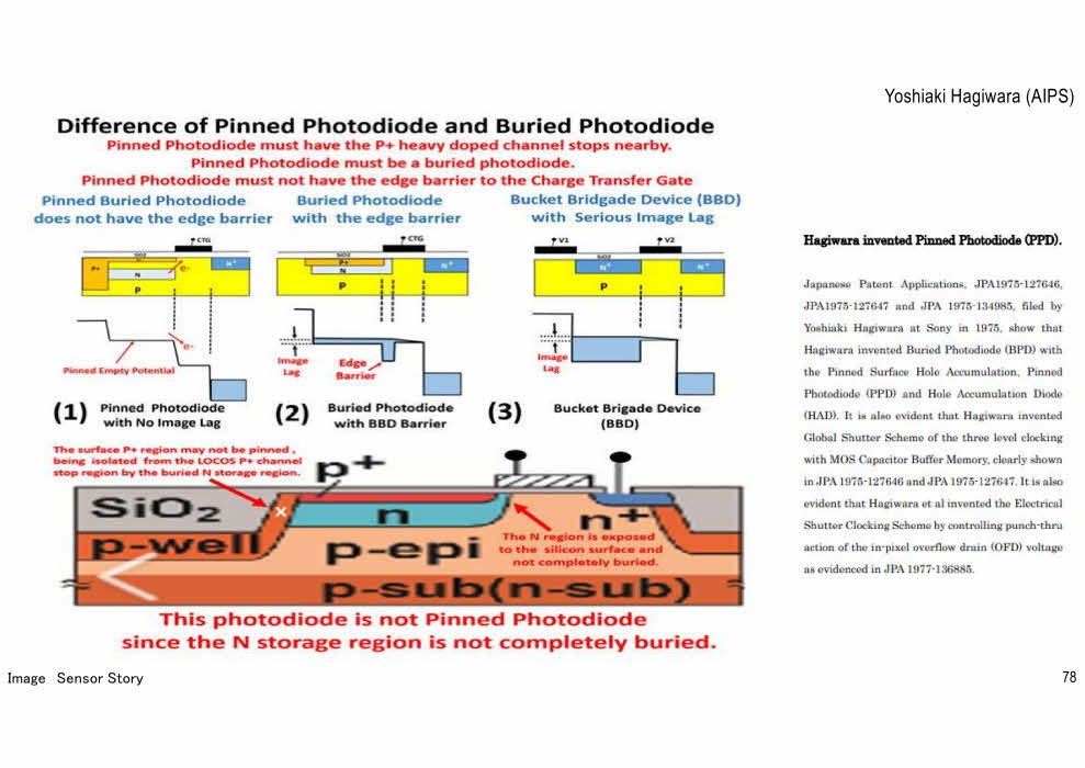
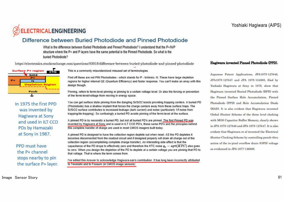
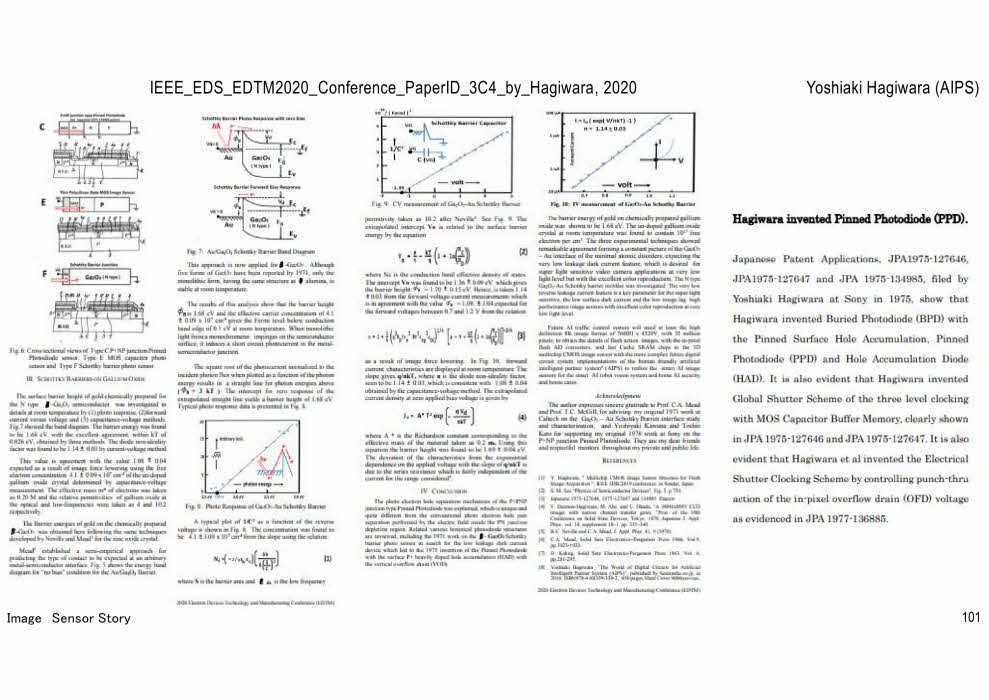
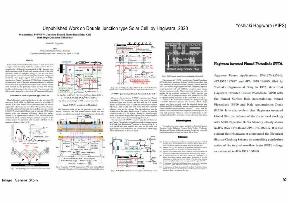
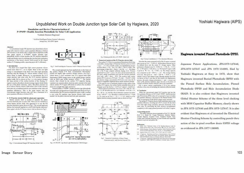
What is the difference of Pinned Photodiode(PPD) and Buried Photodiode(BPD) ?
++++++++++++++++++++++++++++++++++++++++++++++++++++++++++++++++++++++++++
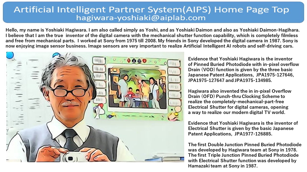
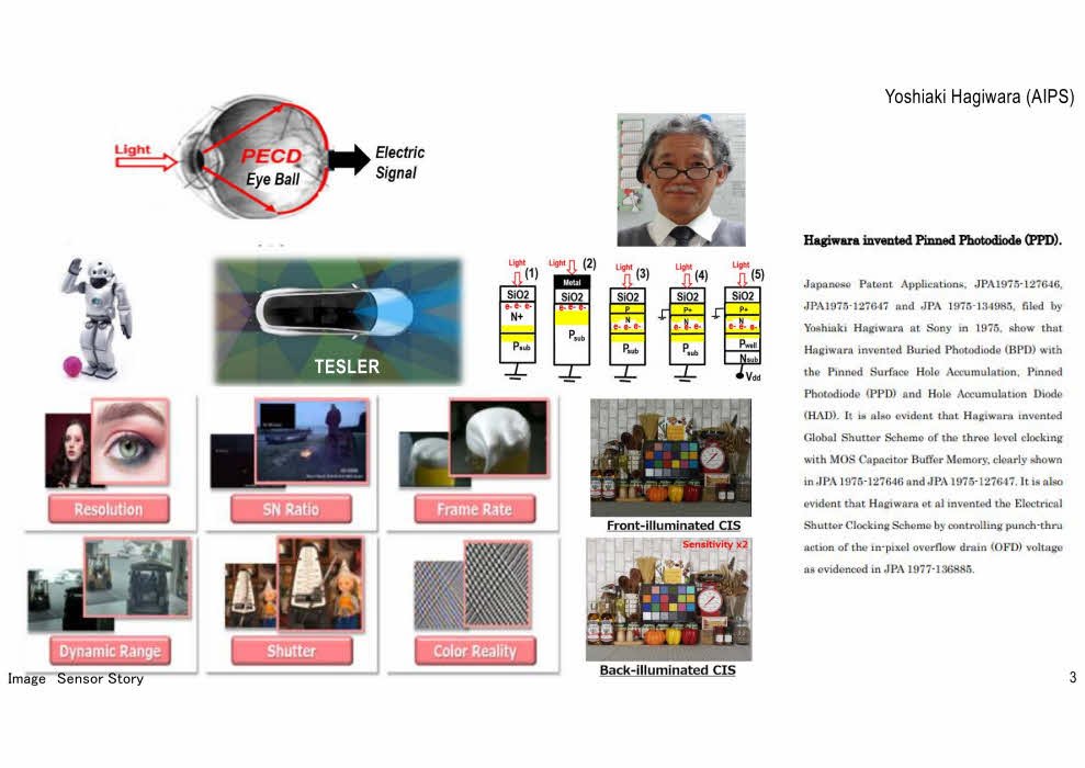
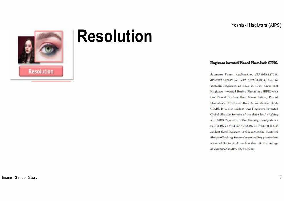
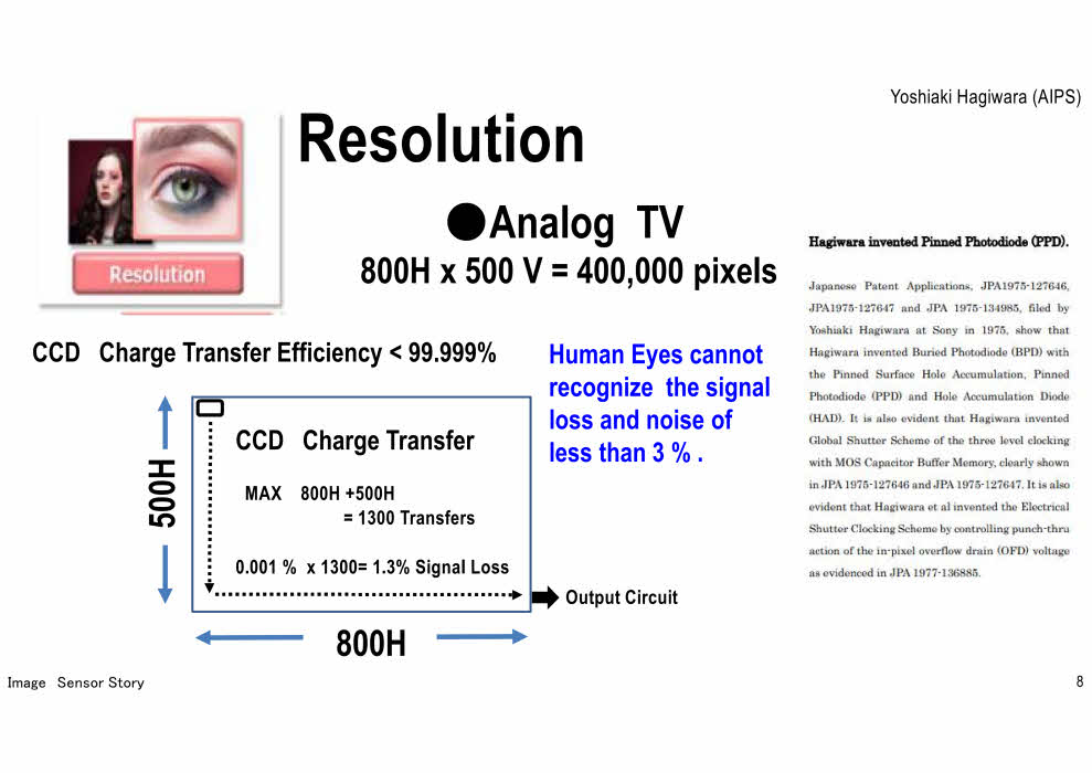
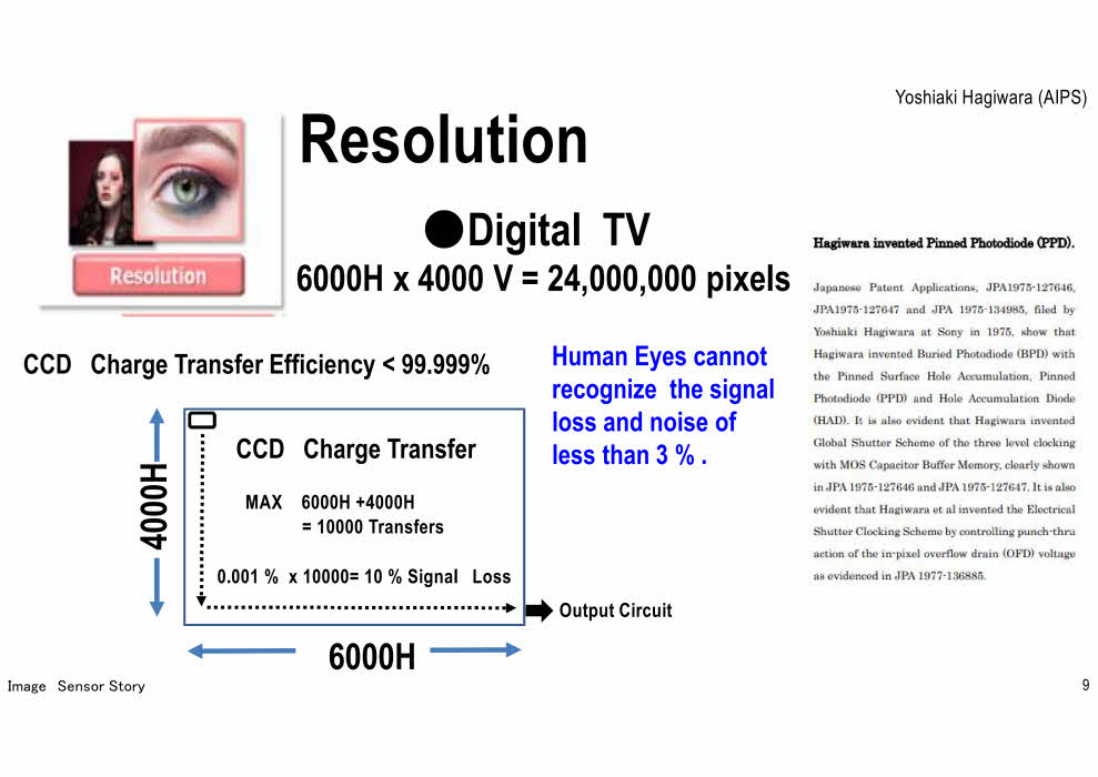
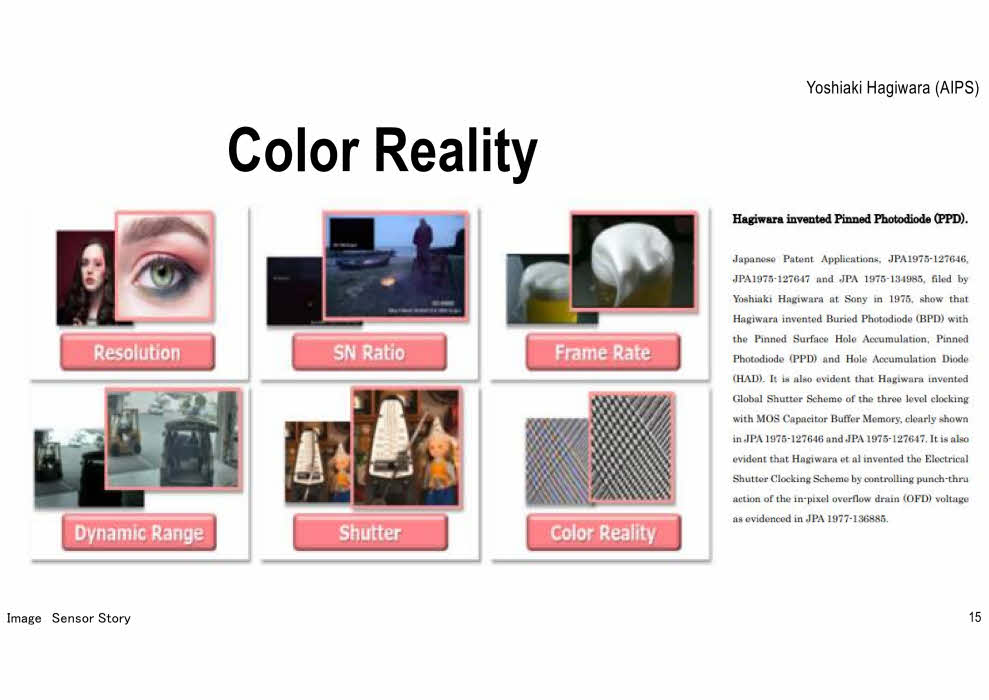
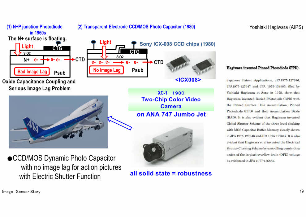
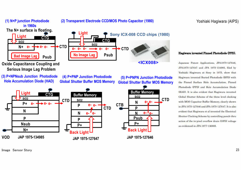
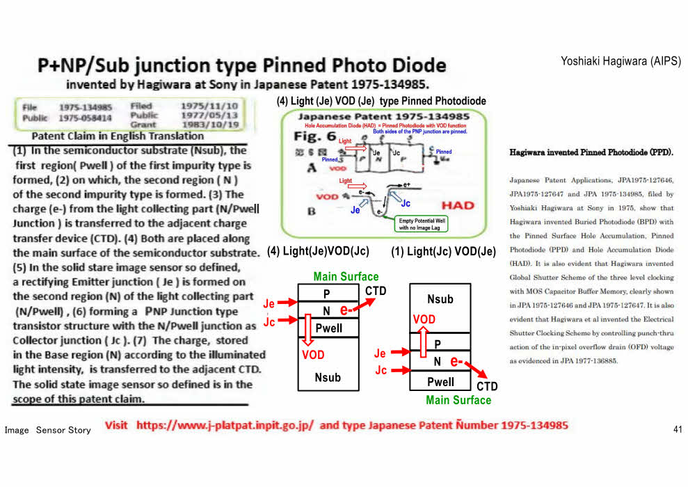
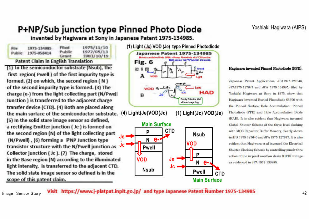
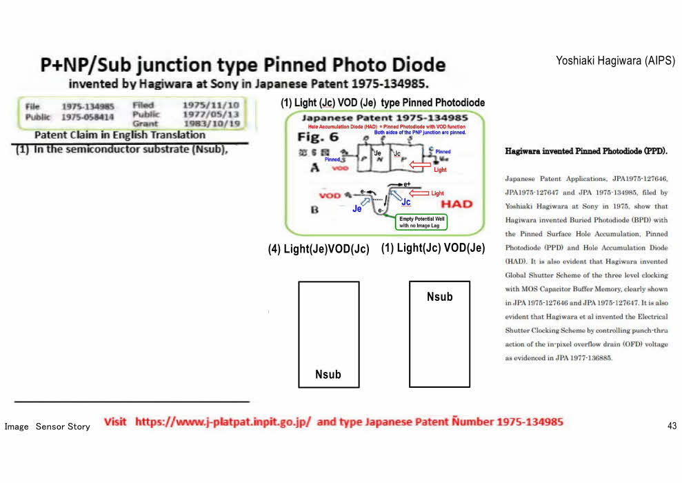
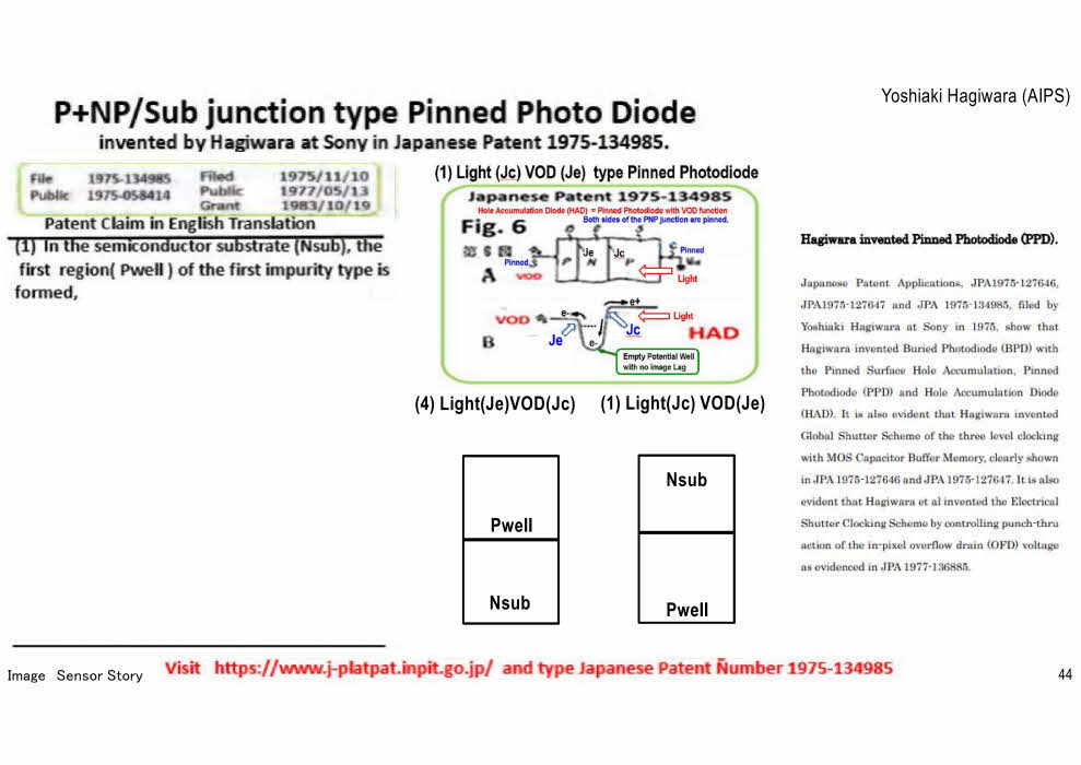
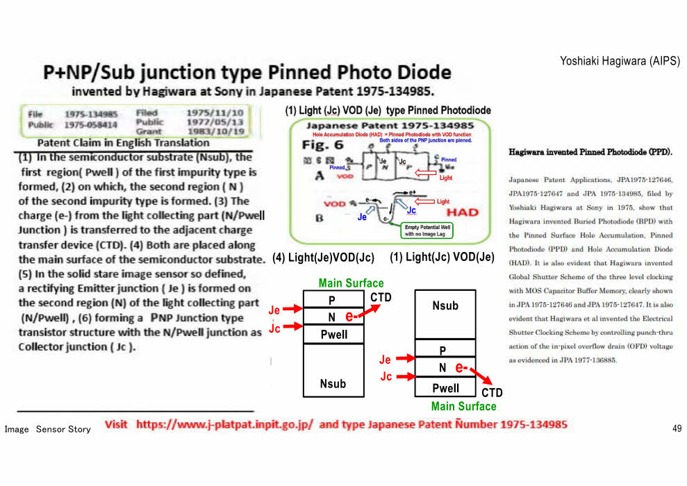
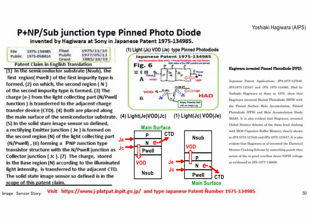
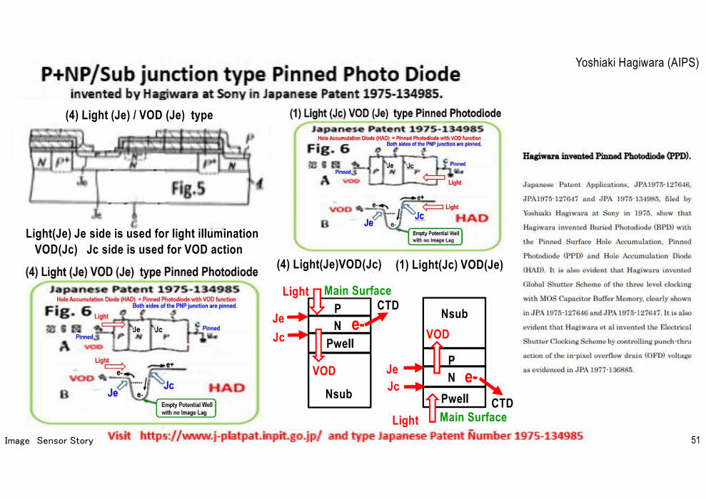
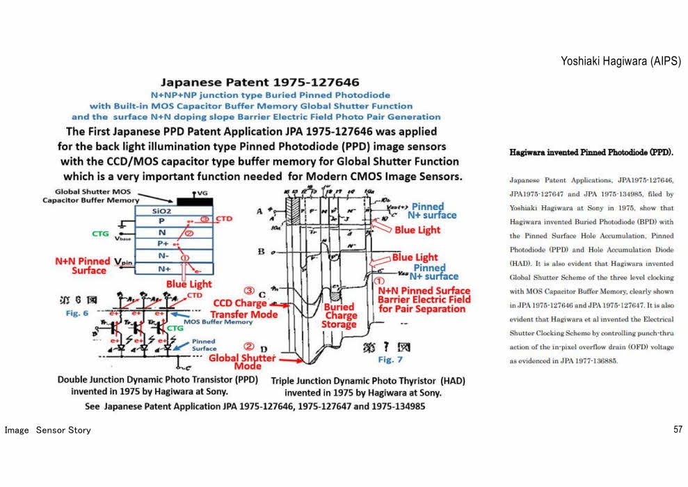
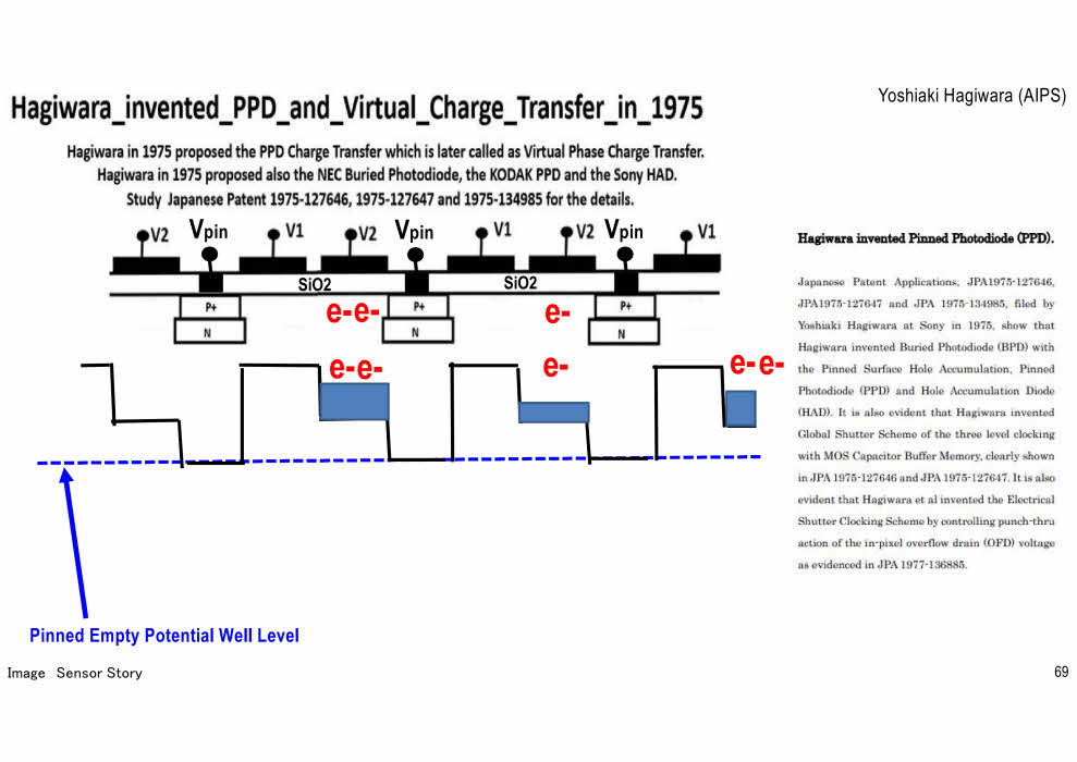
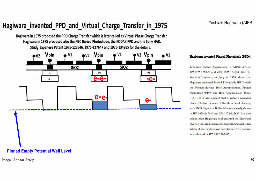
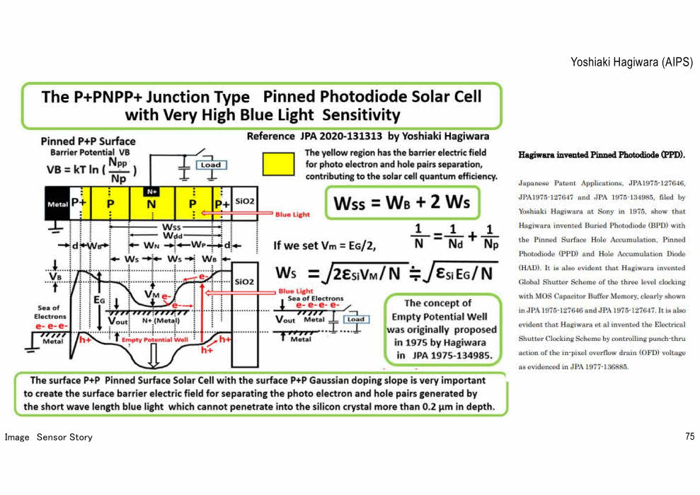
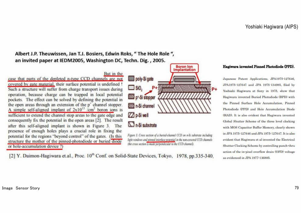
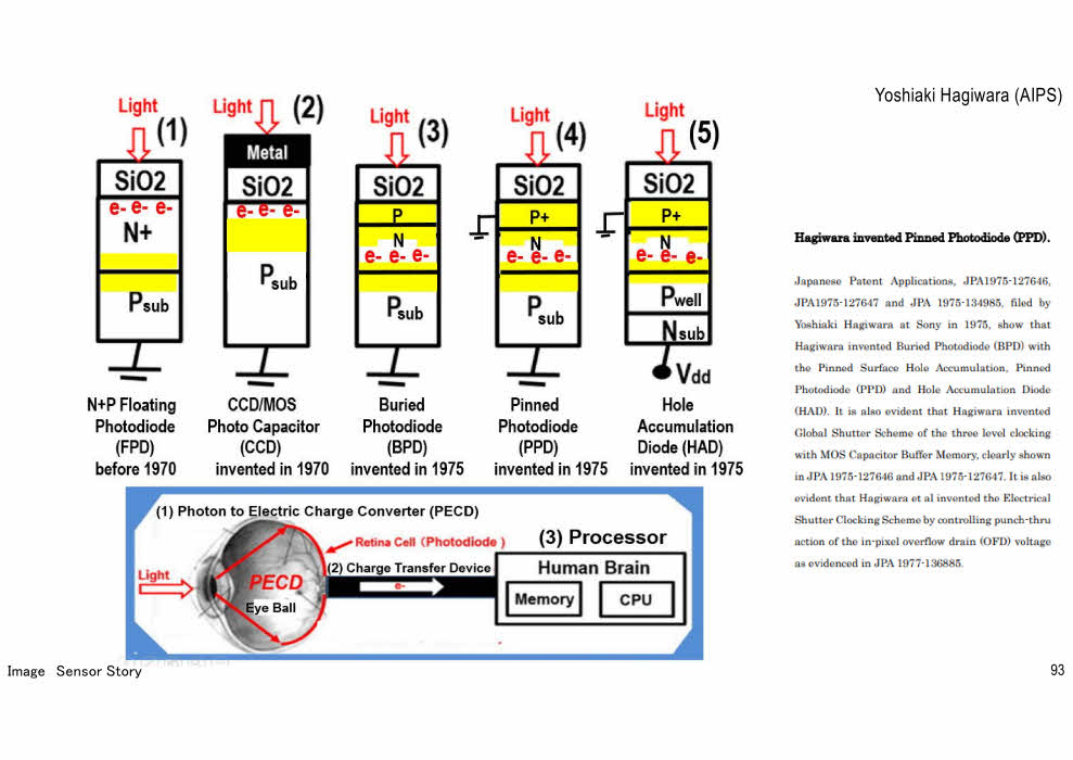
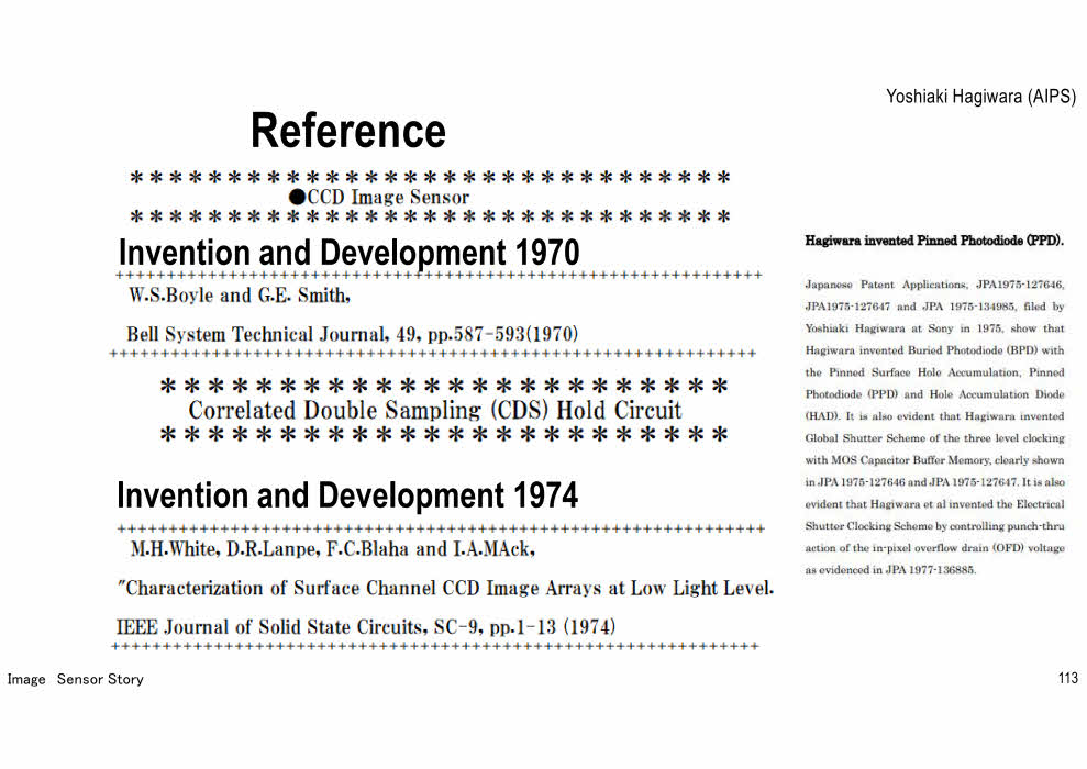
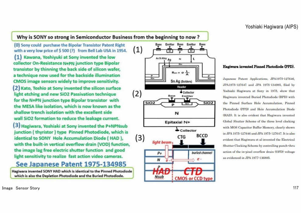
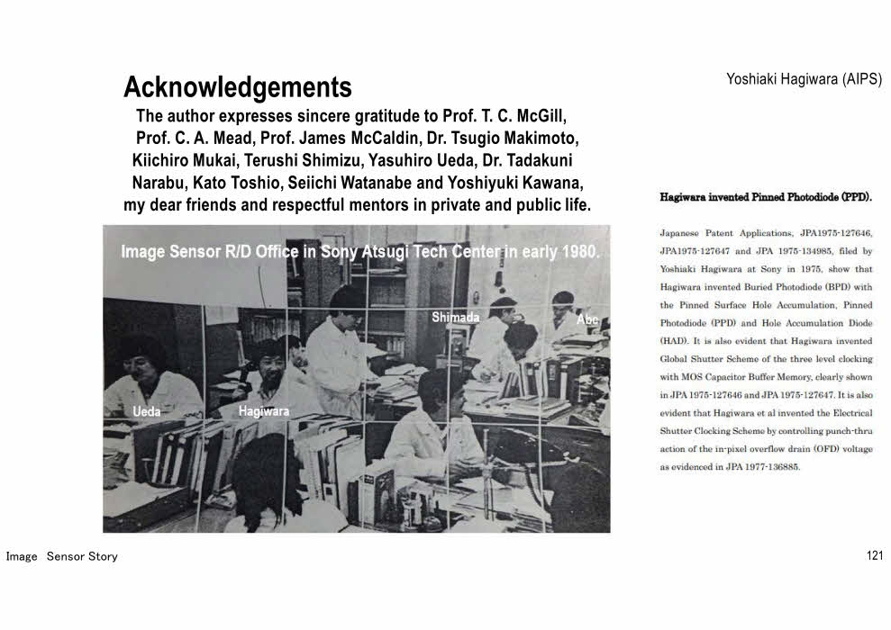
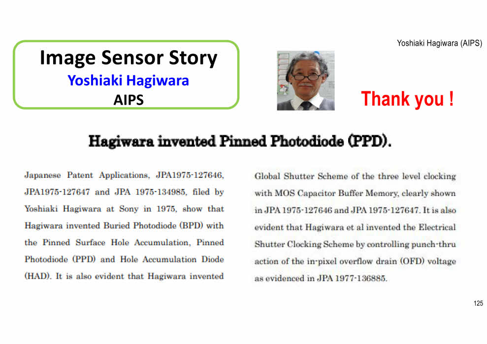
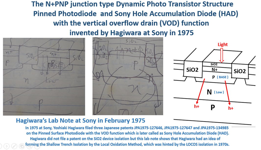
Buried Photodiode (BPD) was invented by Yoshiaki Hagiwara at sony in 1975
as a double junction type PNP photodiode.
JP1975-127646.pdf
JP1975-127647.pdf
JP1975-134985.pdf
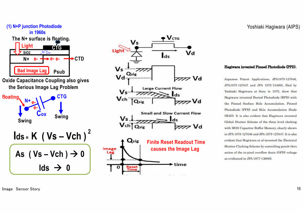
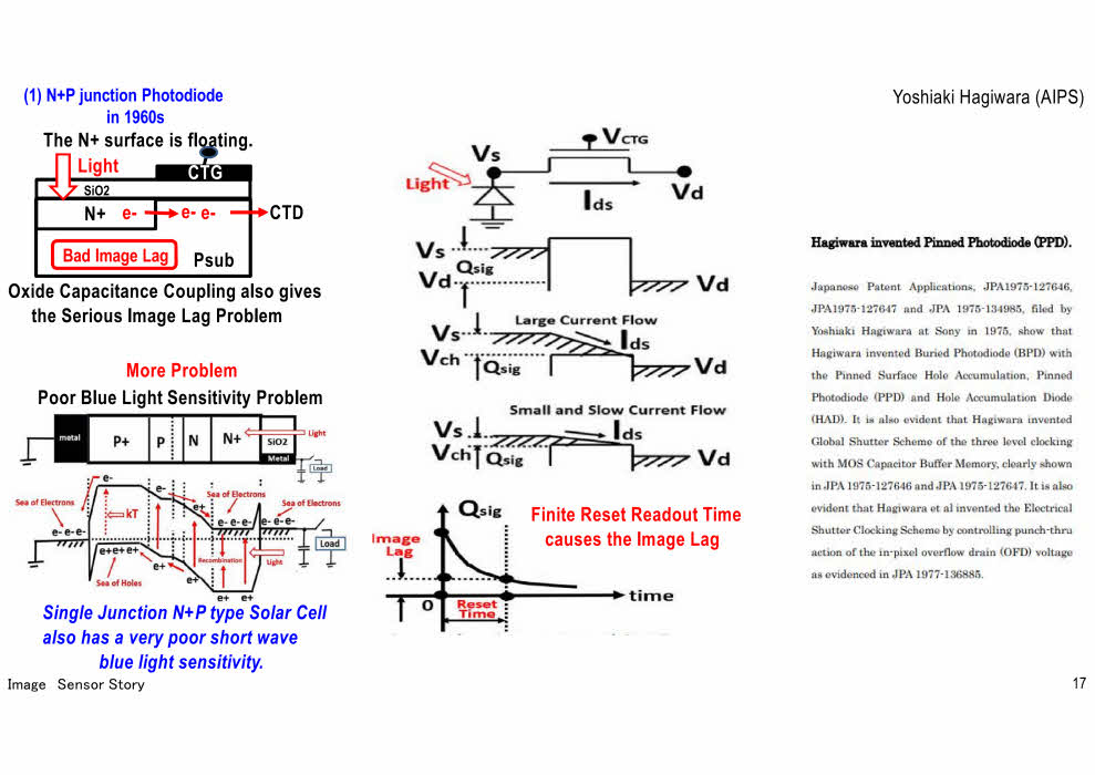
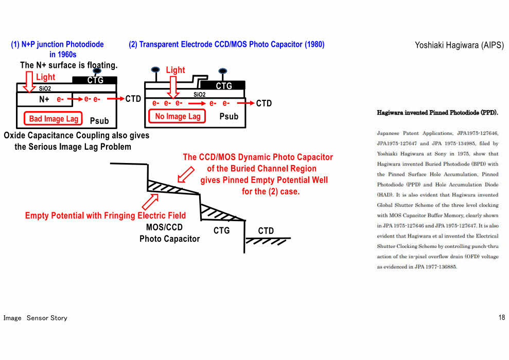
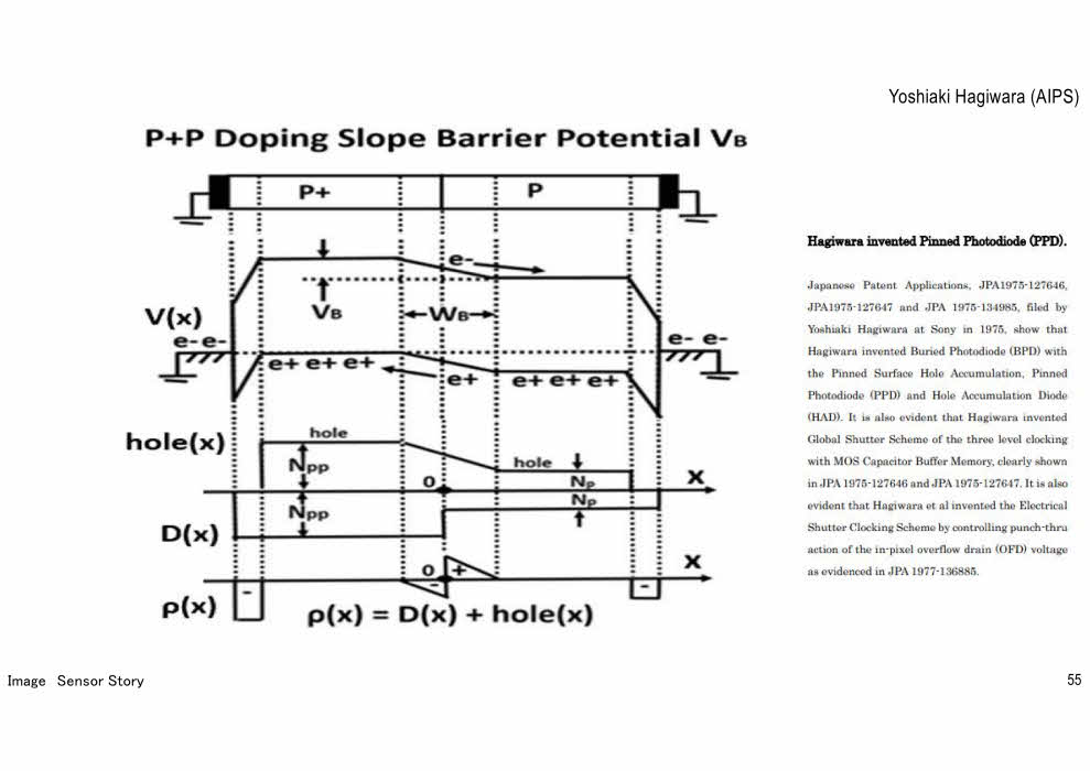
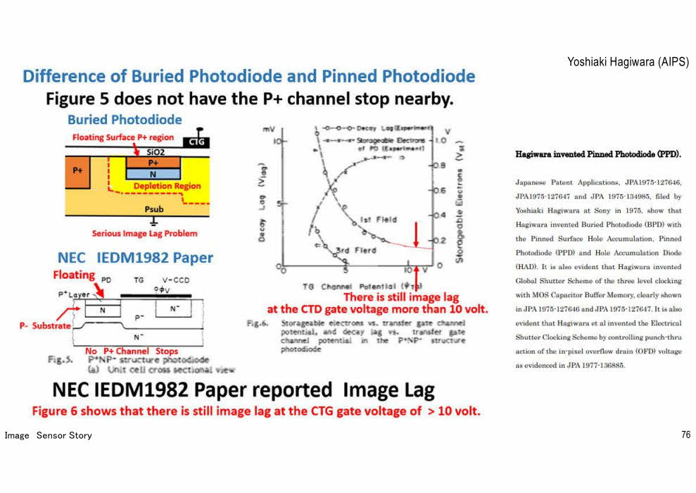
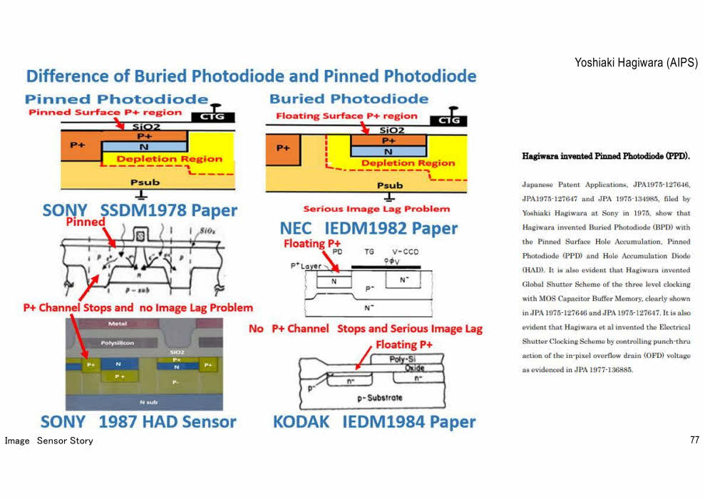
However, Buried Photodiode(BPD) is not always Pinned Photodiode (PPD).
Buried Photodiode(BPD) may not have the Pinned surface p region.
Buried Photodiode(BPD) may have the serious image lag problem.
Buried Photodiode(BPD) may have the serious surface dark curent
when the surface is completely depleted and has the surface strong electric field
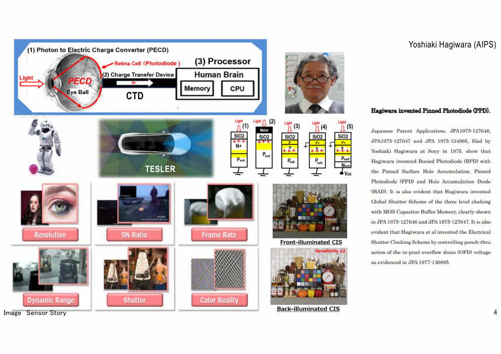
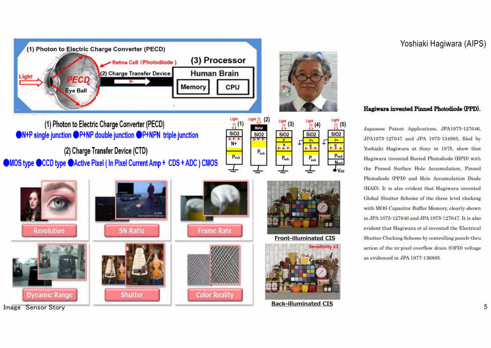
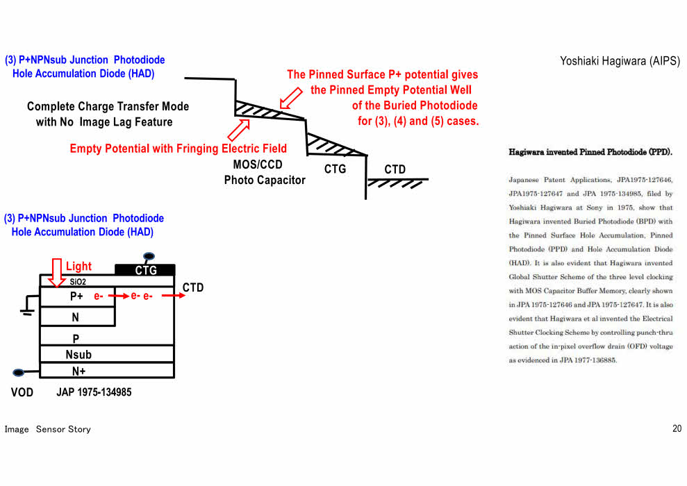
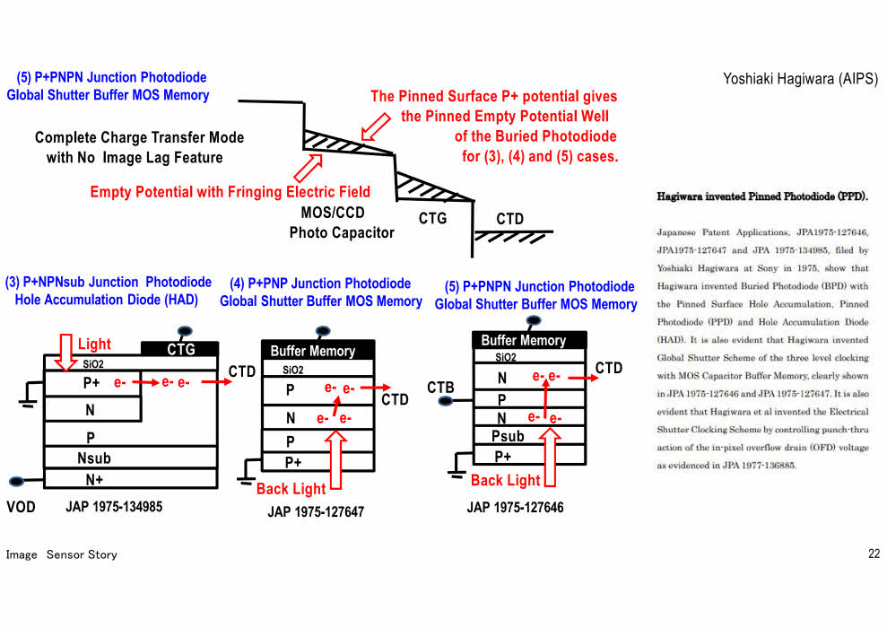
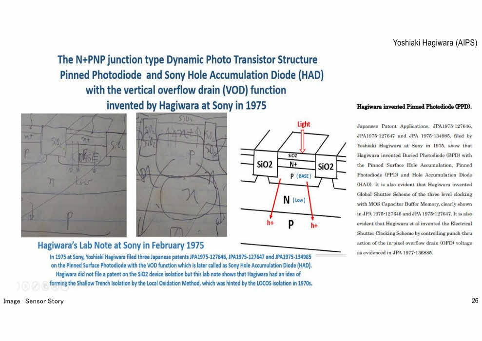
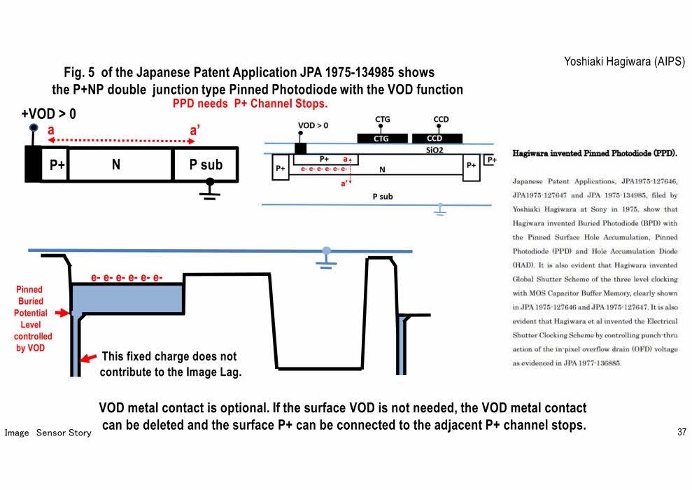
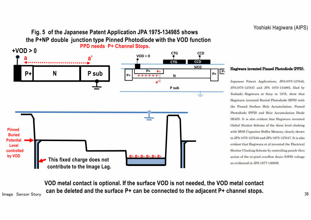
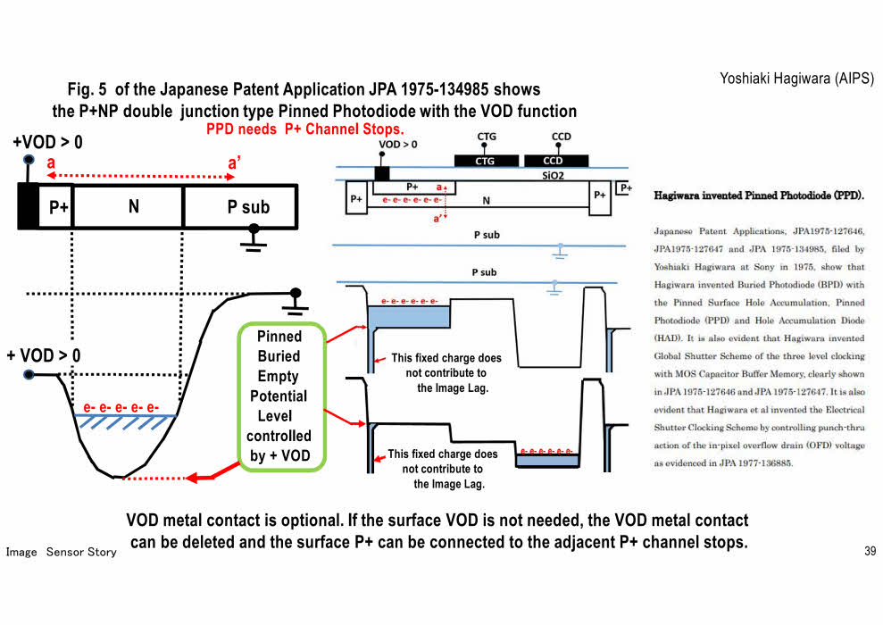
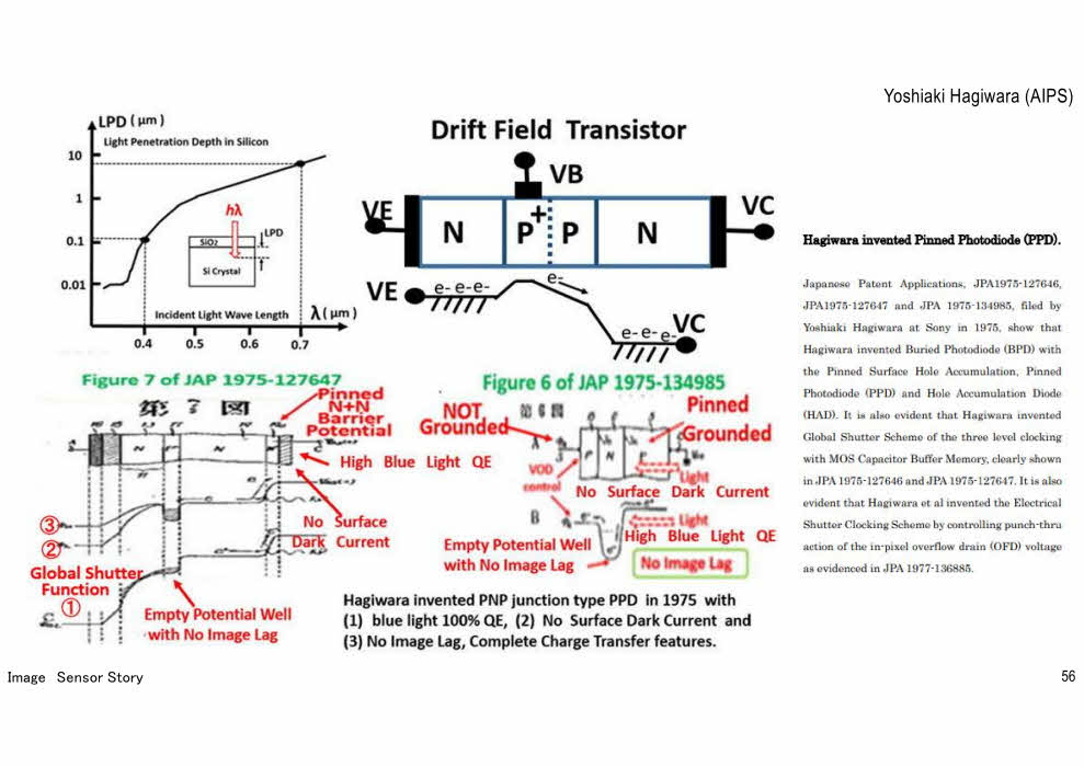
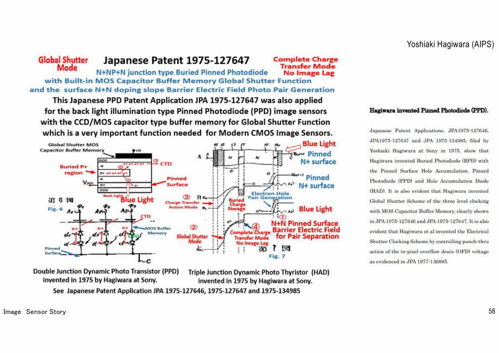
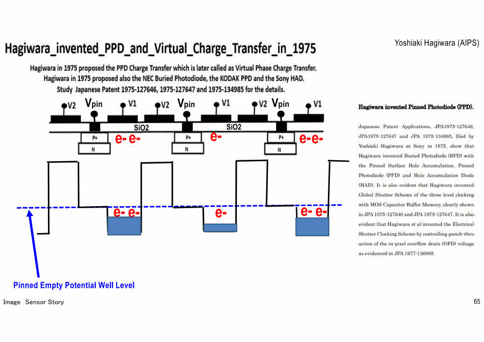
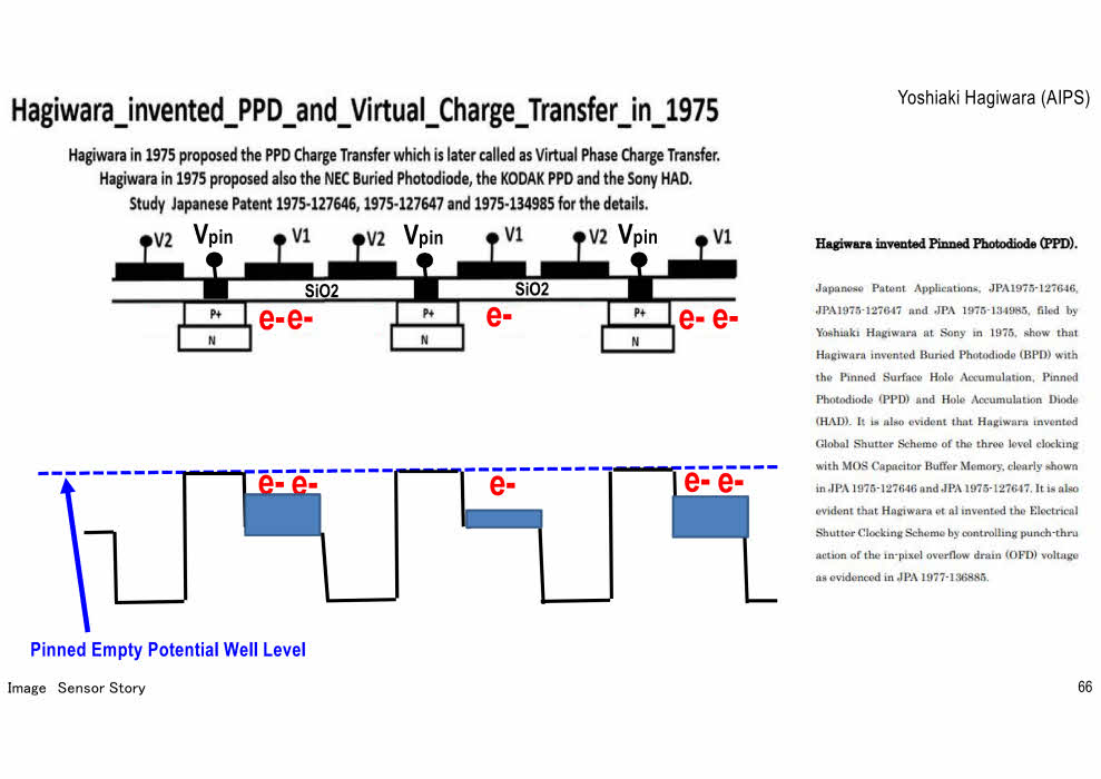
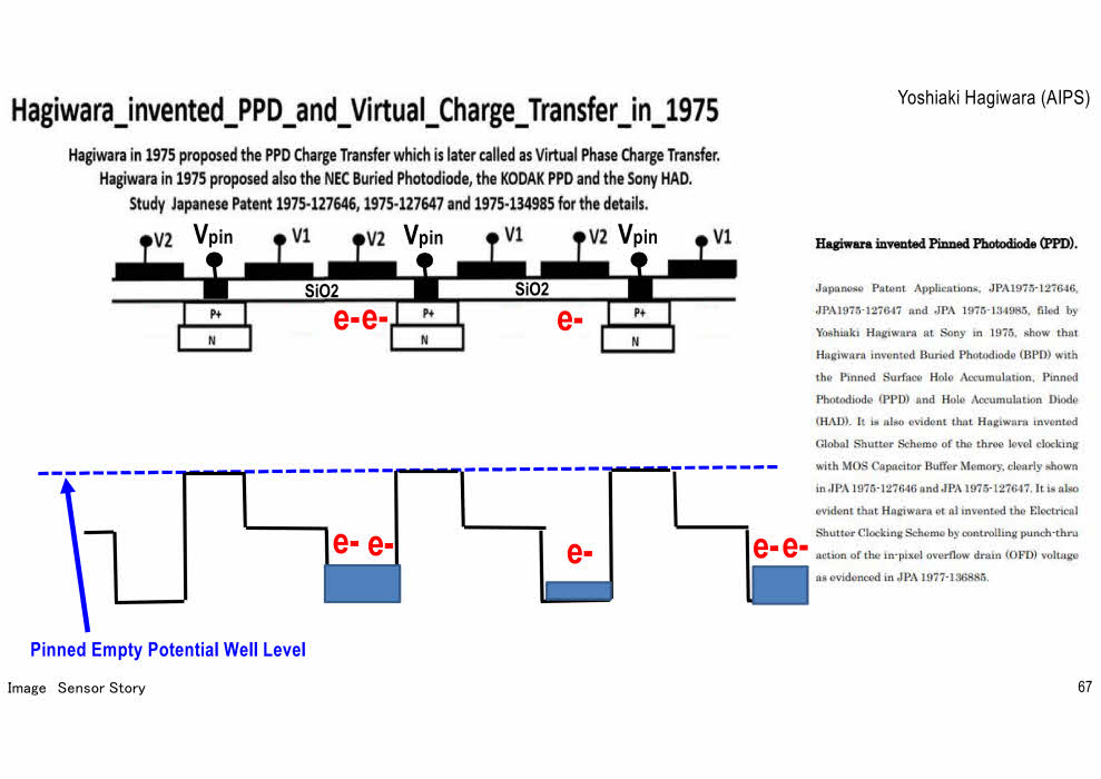
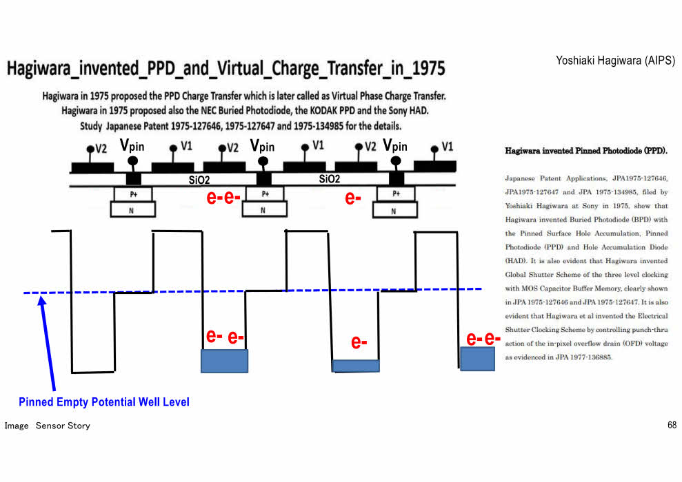
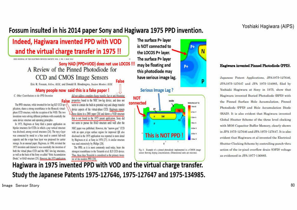
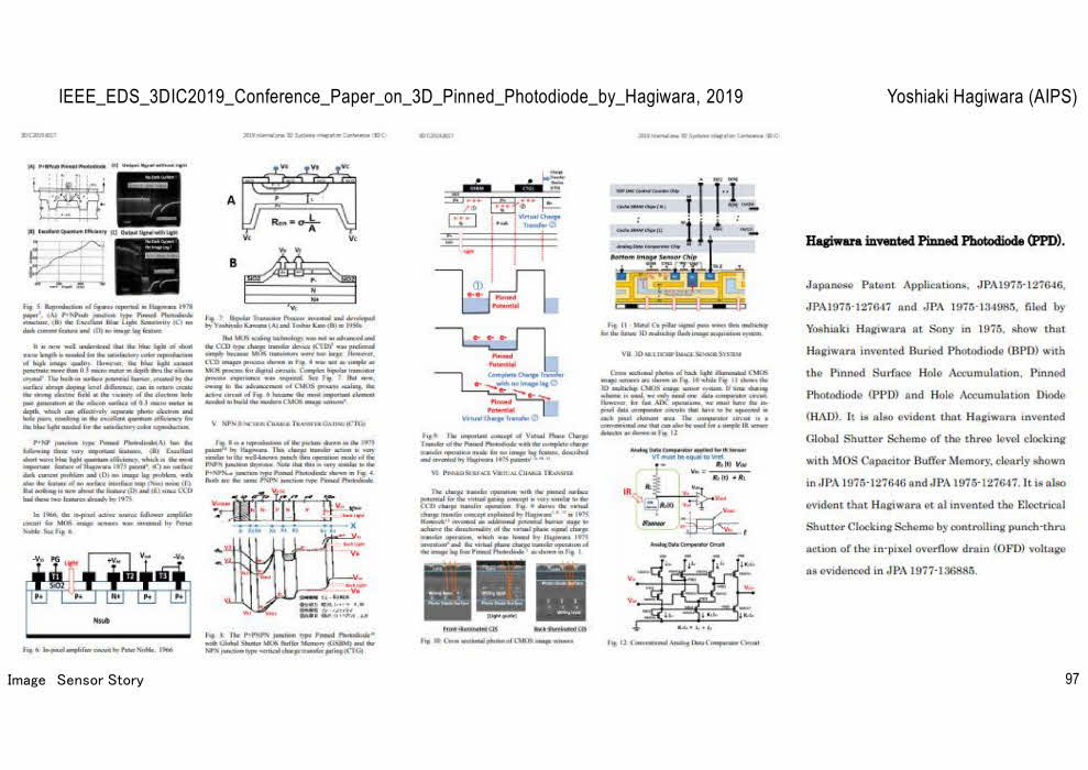
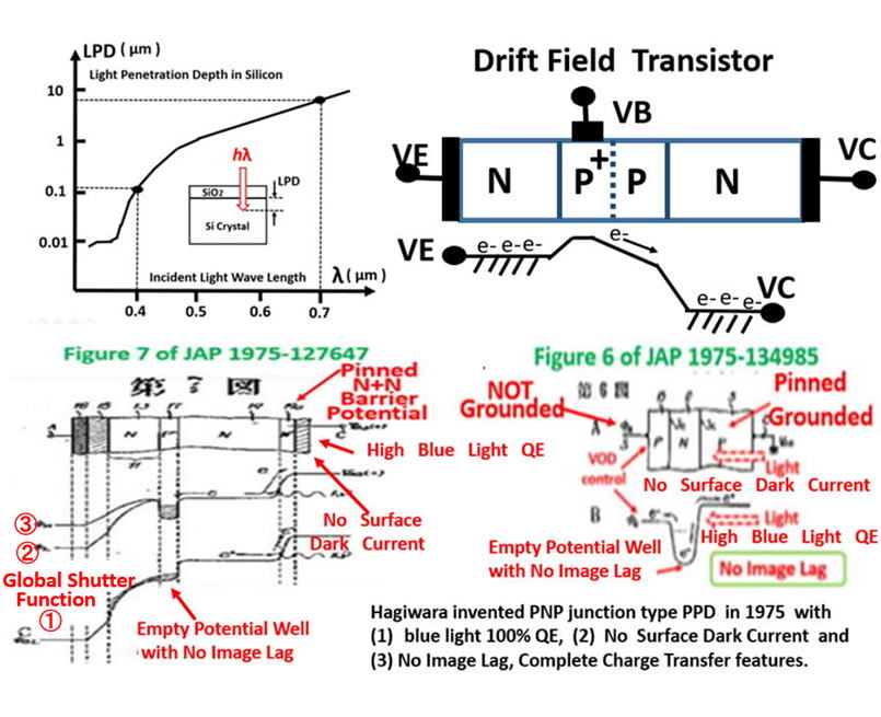
Pinned Photodiode (PPD) was also invented by Yoshiaki Hagiwara at Sony in 1975
in JPA 1975-127646 as a double junction type N+N-P+NP-P Buried Photodiode
and in JPA 1975-127647 as a triple junction type N+N-P+N Buried Photodiode
with the Pinned Surface N+N barrier electric field in the surface electron accumulation region
of the excellent short wave blue light sensitivity,
the very low surface dark current noise, and
the complete charge transfer capability of no image lag feature.
JP1975-127646.pdf
JP1975-127647.pdf
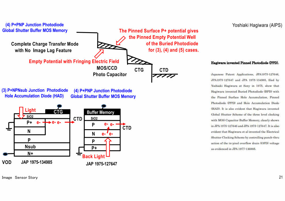
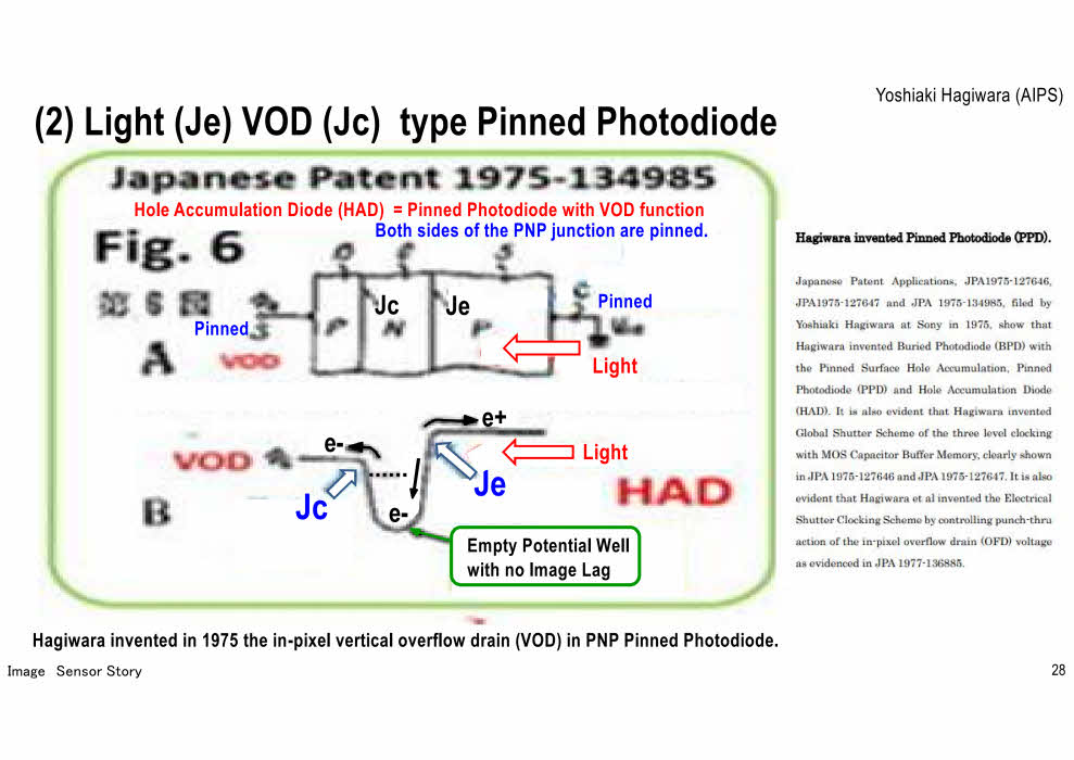
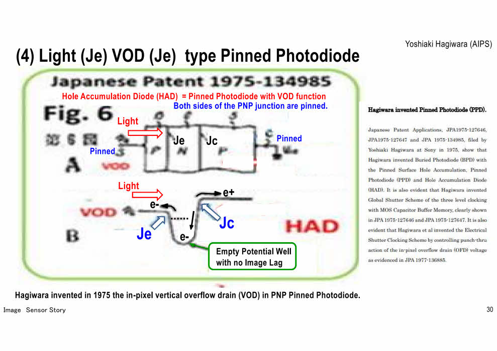
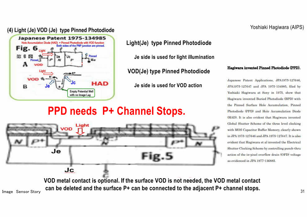
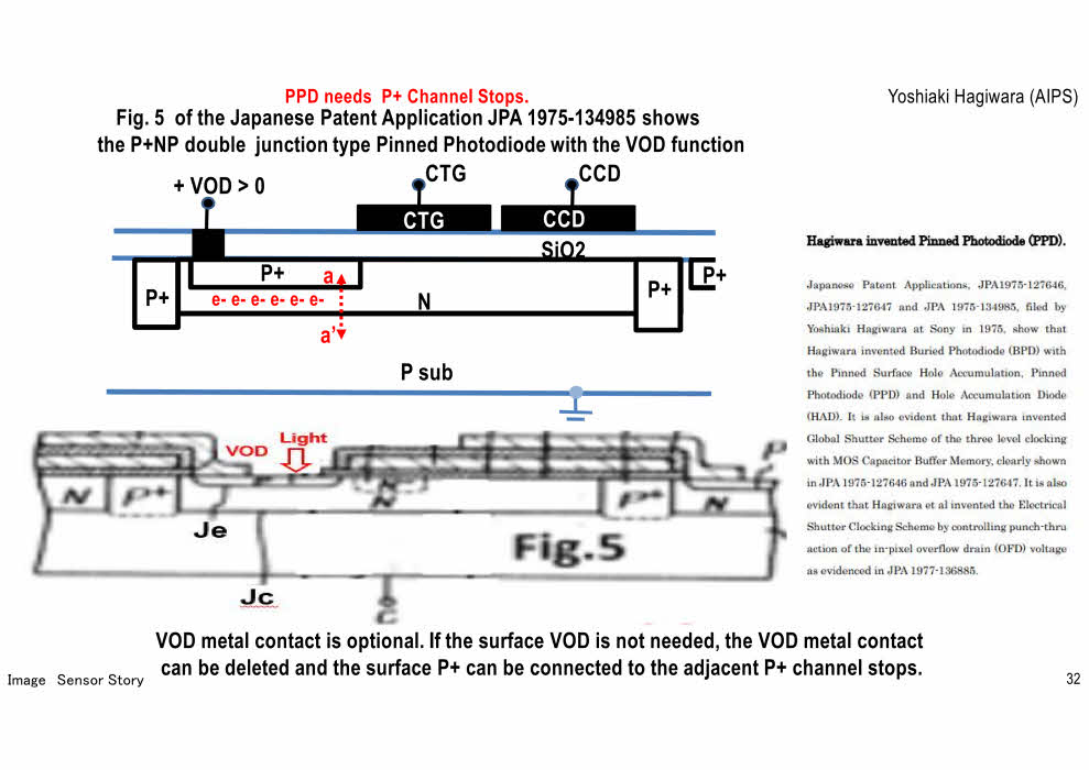
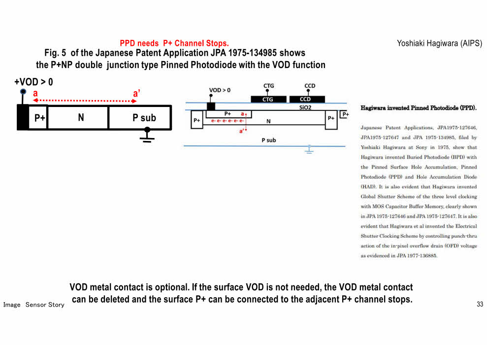
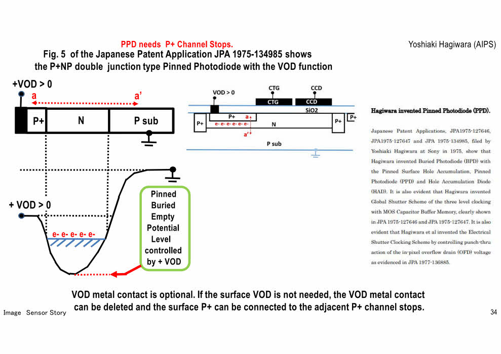
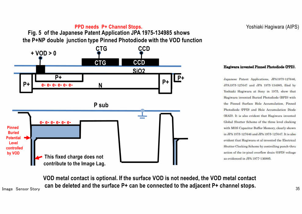
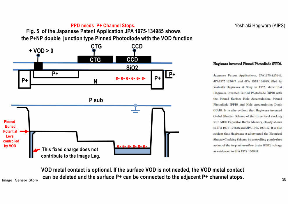
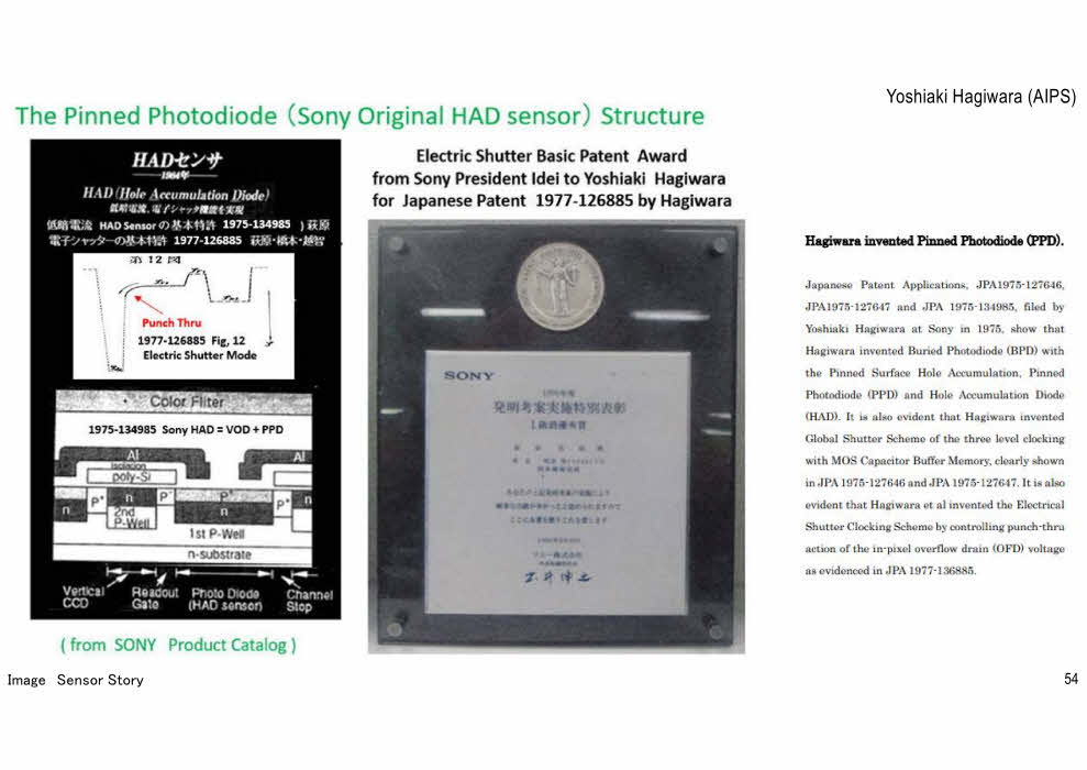
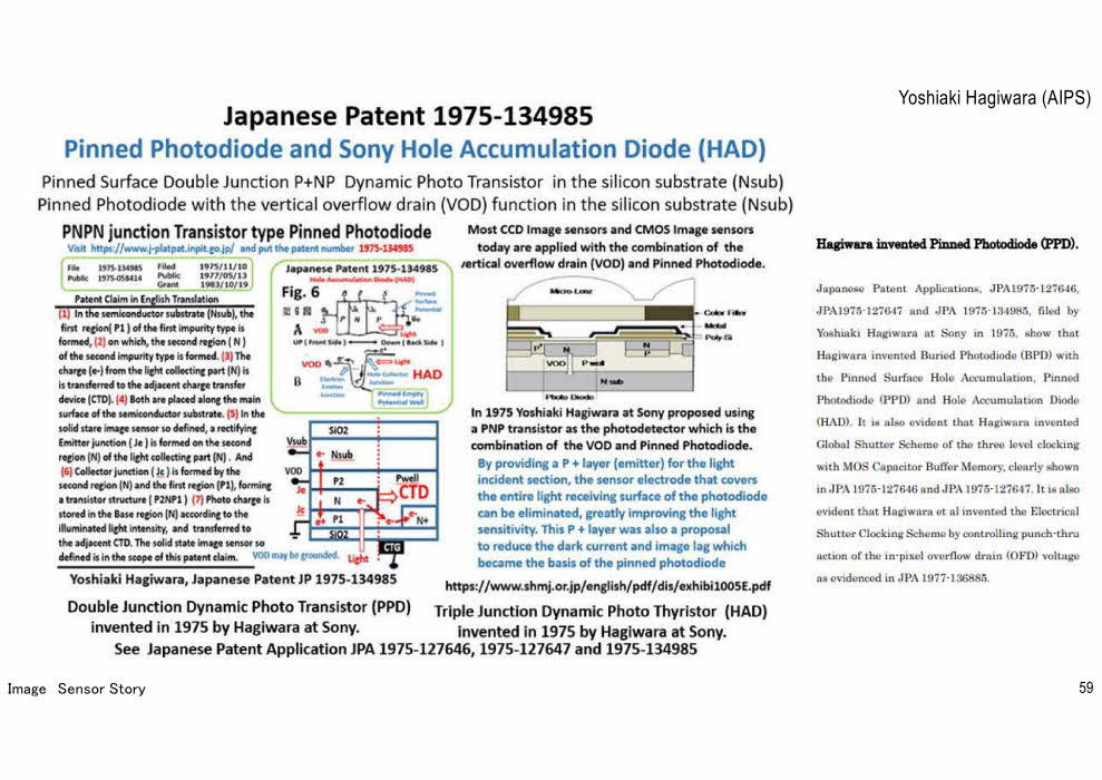
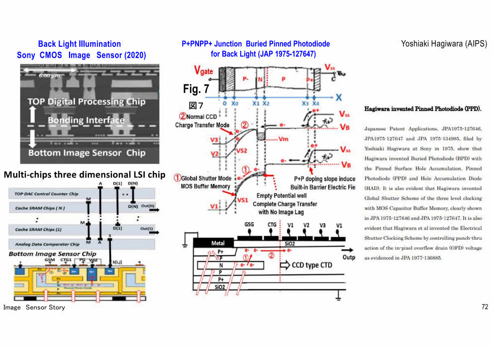
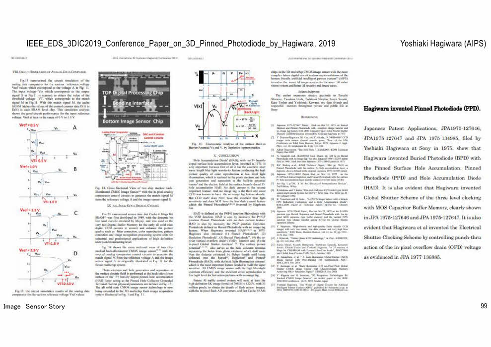
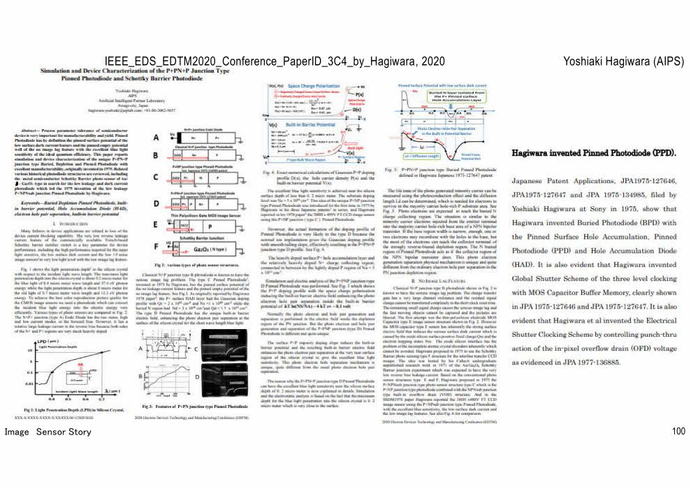
A triple junction type P+NPNsub Pinned Photodiode,
which is a double junction type P+NP Pinned Photodiode in the N type Silicon substrate Nsub,
was also invented in JPA 1975-134985 by Yoshiaki Hagiwara at Sony in 1975
with the built-in vertical overflow drain (VOD) capability.
JP1975-134985.pdf
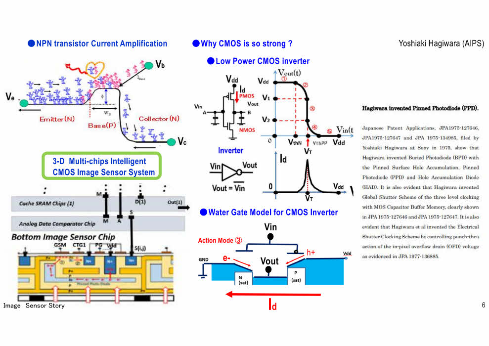
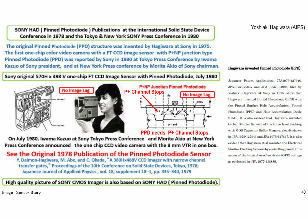
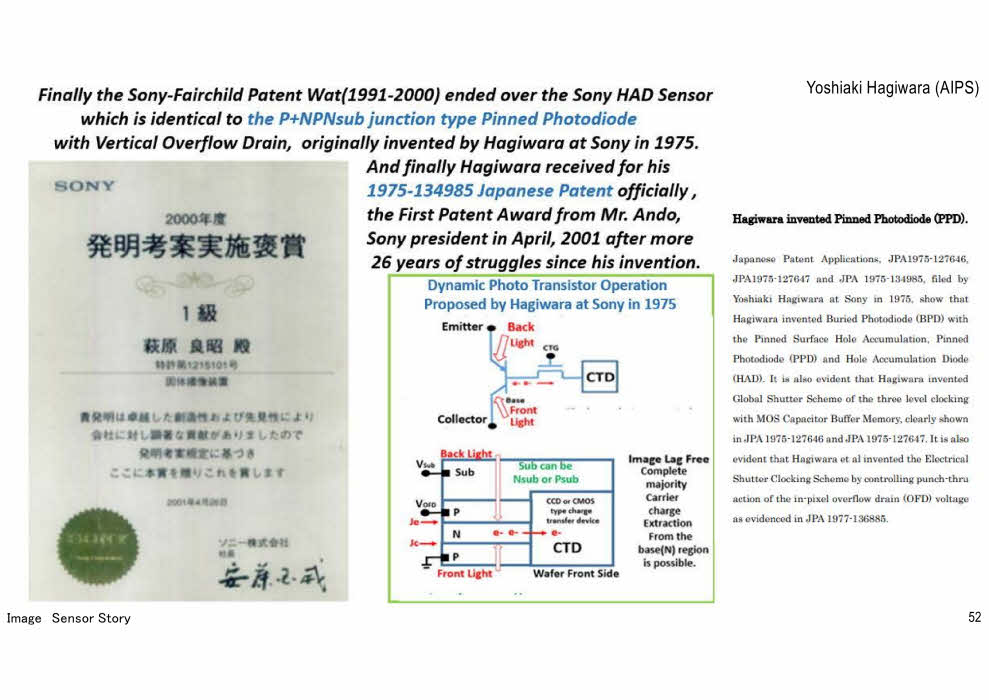
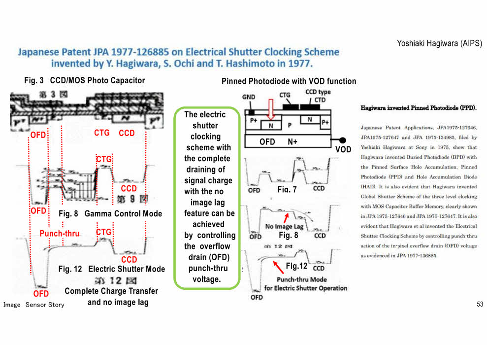
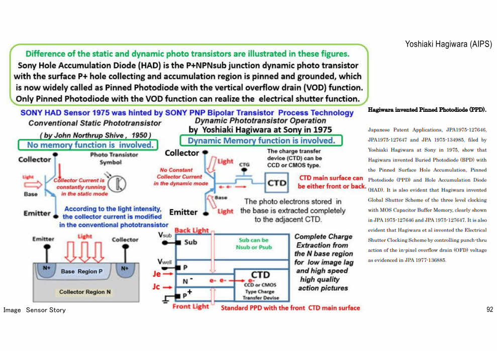
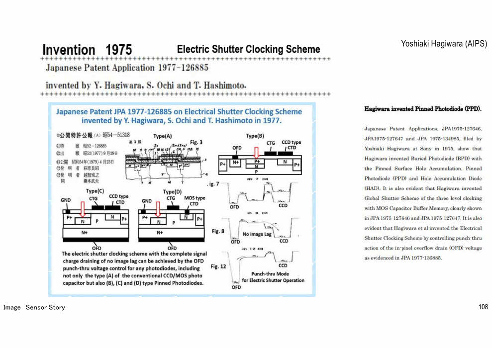
Electrical Shutter Function Clocking Scheme
of controling the punch thru voltage of the built-in verical overflow drain (VOD)
was also invented in JPA 1975-126885 by Yoshiaki Hagiwara at Sony in 1977
and was applied in the triple junction type P+NPNsub Pinned Photodiode
which was named in 1987 as Hole Accumulation Diode(HAD) by Sony Hamazaki Team .
JP1977-126885.pdf
+++++++++++++++++++++++++++++++++++++++++++++++++++++++++++++++++++++++++++++++
+++++++++++++++++++++++++++++++++++++++++++++++++++++++++++++++++++++++++++++++
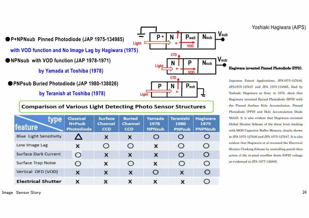
JP1977-837_Hitachi_Koike.pdf
JP1978-1971_Toshiba_Yamada_VOD_patent.pdf
JP1980-138026_NEC_Teranishi_Patent.pdf
+++++++++++++++++++++++++++++++++++++++++++++++++++++++++++++++++++++++++++++++
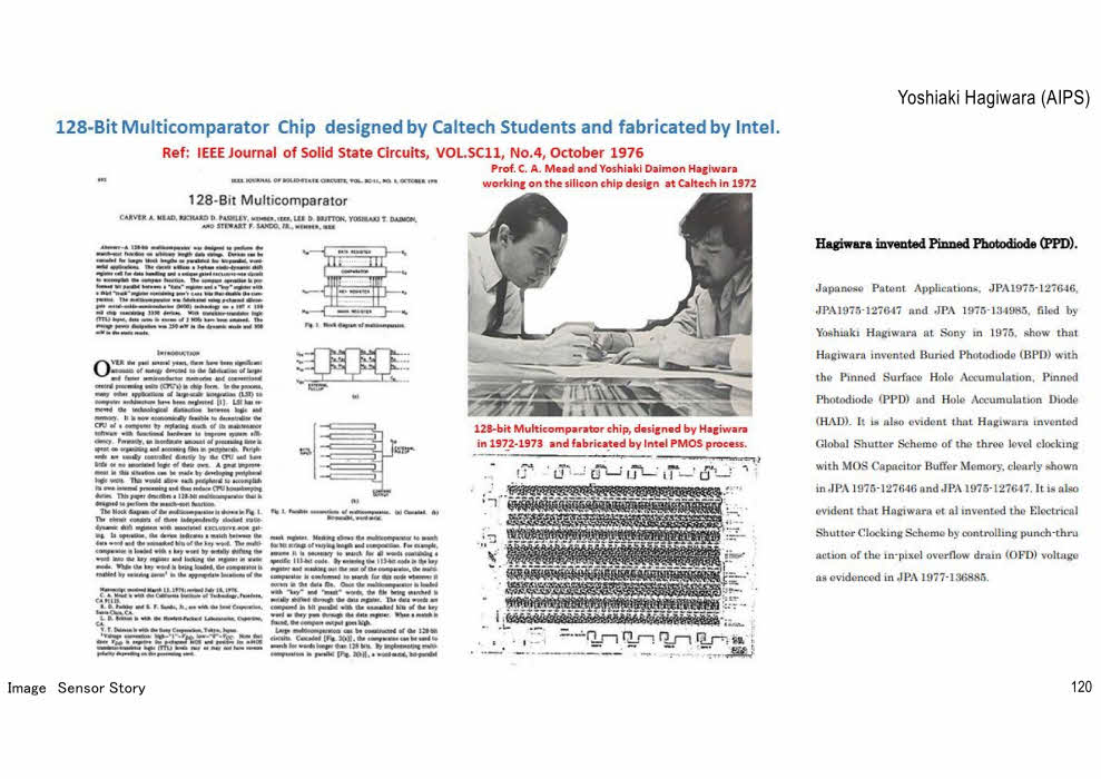
P1976_128_bit_Comparator.pdf
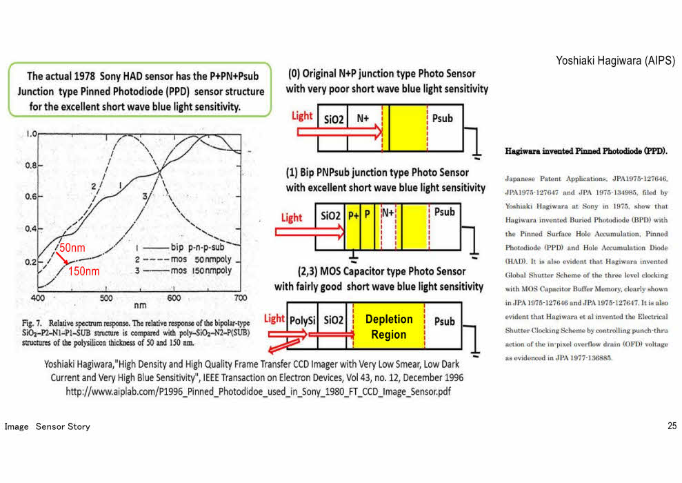
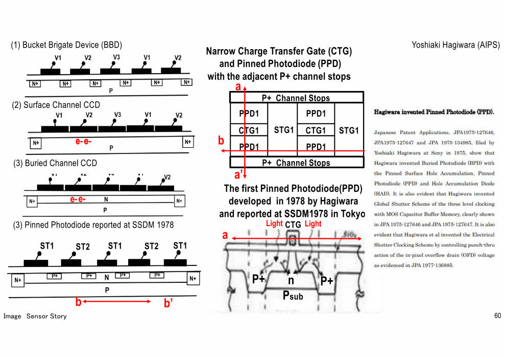
P1978_Pinned_Photodiode_1978_Paper_by_Hagiwara.pdf
P1979_CCD79_in_Edinburgh_1979.pdf
P1989_SONY_4MSRAM_1989.pdf
P1996_Pinned_Photodidoe_used_in_Sony_1980_FT_CCD_Image_Sensor.pdf
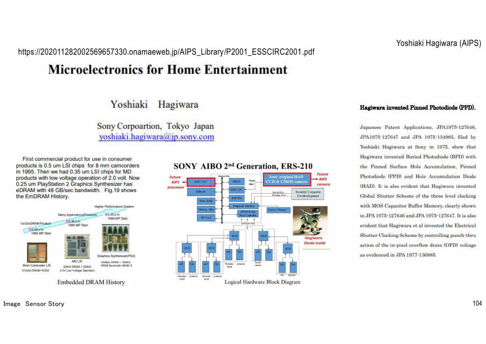
P2001_ESSCIRC2001.pdf
P2008_ESSCIRC2008Hagiwara.pdf
P2013_ISSCC2013PanelTalk.pdf
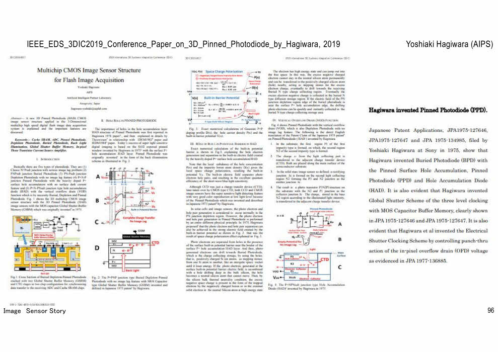
P2019_3DIC2019Paper_on_3D_Pinned_Photodiode.pdf
P2020_EDTM2020_PaperID_3C4_by_Hagiwara.pdf
P2020_Pinned_Photodiode_Solar_Cell_1.pdf
P2020_Pinned_Photodiode_Solar_Cell_2.pdf
+++++++++++++++++++++++++++++++++++++++++++++++++++++++++++++++++++++++++++++++
Buried_Photodiode_is_not_always_PPD_Hagiwara_Nov_2020.pdf
Difference_of_Pinned_Photodiode_and_Buiried_Photodiode.pdf
E-mail_Communication_on_Sony_Loral_Patent_War_1996.pdf
E-mail_communication_with_Albert_san_and_Yoshi.pdf
Evidence_that_Hagiwara_is_the_inventor_of_Pinned_Photodiode_2020_10_04a.pdf
Evidence_that_Hagiwara_is_the_inventor_of_Pinned_Photodiode_in_Japanese.pdf
Hagiwara_invented_PPD_and_Sony_HAD_in_1975.pdf
Hagiwara_invented_PPD_and_Sony_HAD_in_1975_2020_08_21.pdf
Hagiwara_invented_PPD_and_Sony_HAD_in_1975_Head.pdff
Image_Sensor_Story_07.pdf
Image_Sensor_Story_14.pdf
Origin_of_1975_Concept_of_Pinned_Photodiode.pdf
The_evidence_that_Hagiwara_is_the_inventor_of_Pinned_Photodiode_2020_10_02 .pdf
+++++++++++++++++++++++++++++++++++++++++++++++++++++++++++++++++++++++++++++++
Hagiwara_invented_PPD_and_Sony_HAD_in_1975.html
+++++++++++++++++++++++++++++++++++++++++++++++++++++++++++++++++++++++++++++++
AIPS Library
+++++++++++++++++++++++++++++++++++++++++++++++++++++++++++++++++++++++++++++++
Past Homepage Backups
2021_01_23
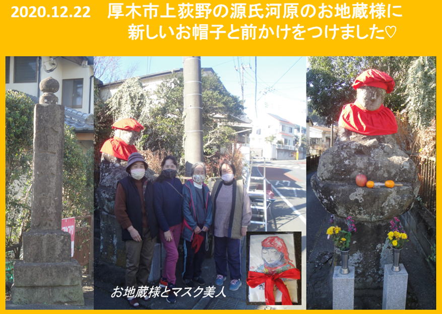
2020_12_22
2020_12_17
2020_12_15
2020_12_09
2020_06_27
2019_09_25
2019_07_12
2018_11_29
*********************************************************************
hagiwara-yoshiaki@aiplab.com for my activity at http://www.aiplab.com/
hagiwara@ssis.or.jp for my activity at http://www.ssis.or.jp/en/index.html
*********************************************************************