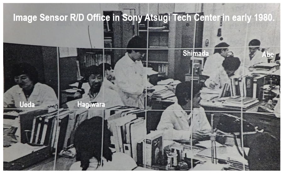
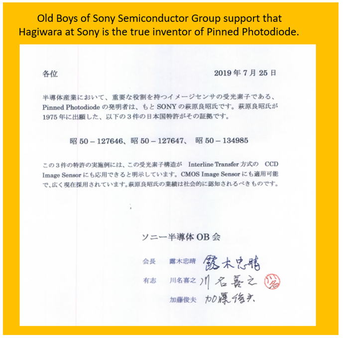
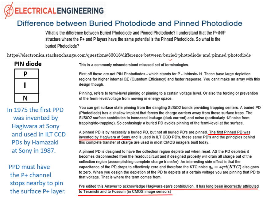
Hagiwara at Sony invented Pinned Photodiode in 1975.
Hagiwara at Sony invented Pinned Photodiode in 1975.
*********************************************************************
Please write me freely anything related to my activities:
*********************************************************************
hagiwara-yoshiaki@aiplab.com for my activity at http://www.aiplab.com/
hagiwara@ssis.or.jp for my activity at http://www.ssis.or.jp/en/index.html
*********************************************************************
SSIS_Educaion_Activity ( Members Only )
*********************************************************************
老人の独り言です
音声でのSlide001 の解説です
音声でのSlide002 の解説です
音声でのSlide003 の解説です
音声でのSlide004 の解説です
音声でのSlide005 の解説です
音声でのJP1975-127646_Aの解説です
JPA 1975-127646.pdf
音声でのJP1975-127647_Aの解説です
JPA 1975-127647.pdf
音声でのJP1975-134985_Aの解説です
JP1975-134985_Patent_Claims_in_English_Translation.pdf
JPA 1975-134985.pdf
音声での JP1977-126885 の解説です
JPA 1977-126885.pdf
https://www.sony.co.jp/SonyInfo/News/notice/20200626/
Sony says "Hagiwara invented PPD in 1975."
SSIS.or.jp also says "Hagiwara proposed Pinned Photodiode in 1975.
*********************************************************************
ソニーのイメージセンサーの発明の歴史は、古くはCCDの時代までさかのぼる。
中でもPinned Photodiodeは、裏面照射型CMOSセンサーの性能向上にも貢献する
技術であり、その発明と製品開発の歴史を紐解く。
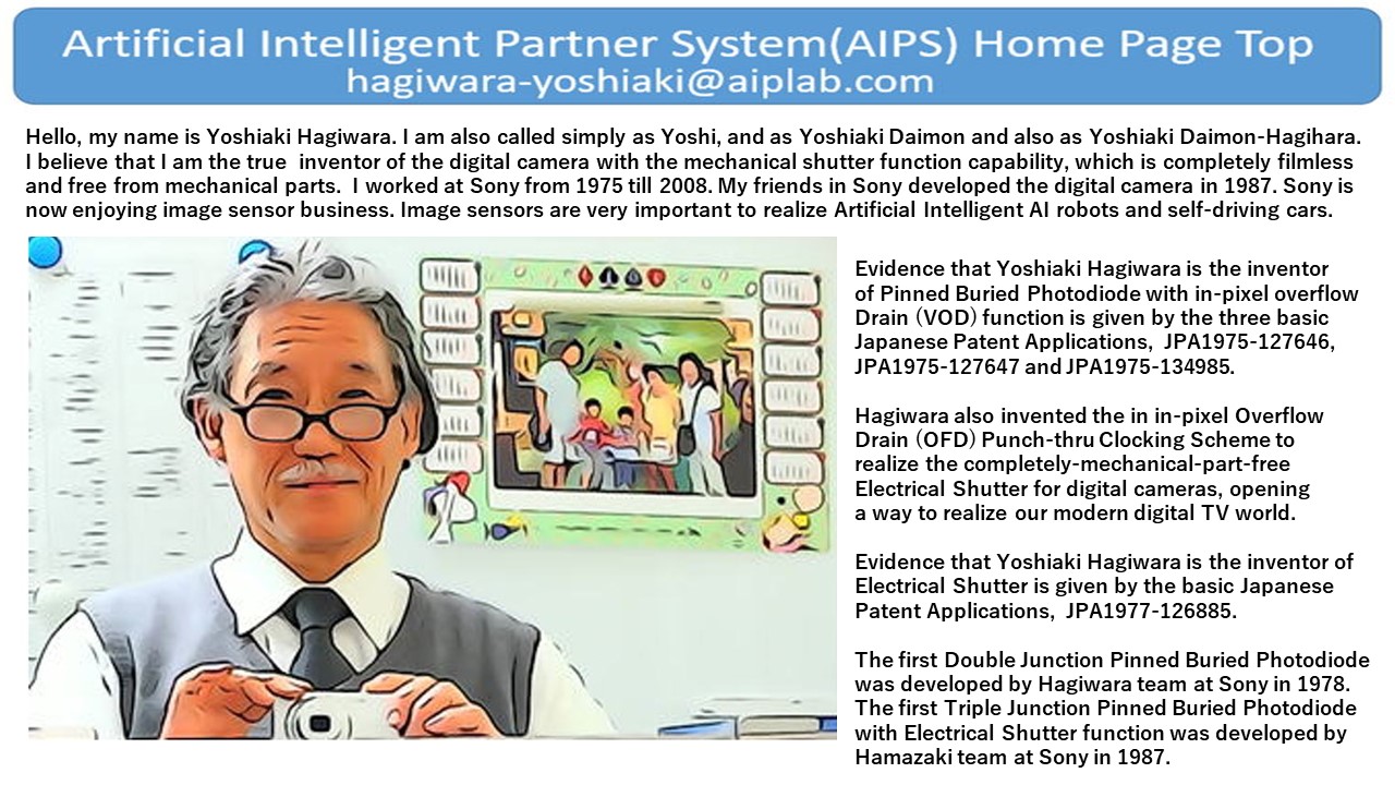
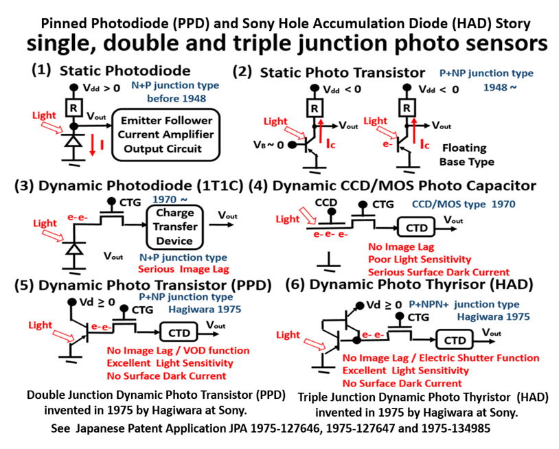
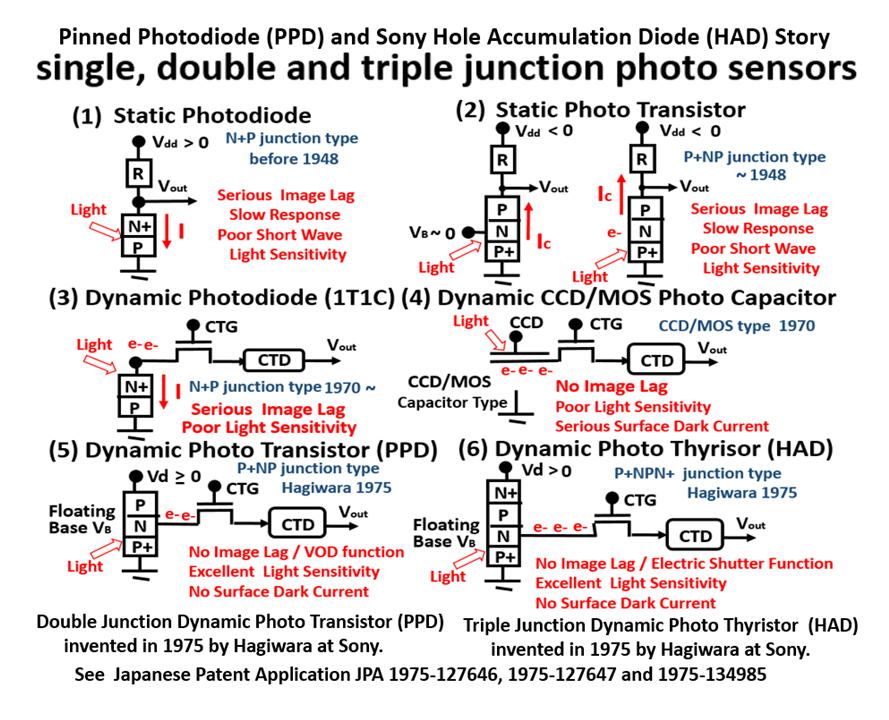
ソニーは1975年、裏面照射型のN+NP+N接合型とN+NP+NP接合型の
Pinned Photodiode(PPD)を採用したCCDイメージセンサーを発明
した(出願特許1975-127646,1975-127647 萩原 良昭)。
同年、その構造をヒントに、VOD(縦型オーバーフロードレイン)機能を持つ、
PNP接合型PPDを発明した(特許第1215101号 萩原 良昭)。
ソニーはその後、イオン打ち込み技術により濃いP+のチャンネルストップ領域を
その受光部近傍に形成したPNP接合型のPPD技術を採用したフレームトランス
ファー型CCDイメージセンサーの原理試作に世界で初めて成功し、1978年の
SSDM1978の学会で論文を発表した(Y. Hagiwara, M. Abe, and C. Okada,
“A 380H x 488V CCD imager with narrow channel transfer gates”, Proc.
The 10th Conference on Solid State Devices, Tokyo, (1978))。
1980年にはソニーはこのPNP接合型PPD を採用したワンチップのフレーム
トランスファーCCDイメージセンサーを使ったカメラ一体型VTRの試作に成功し、
東京では当時社長の岩間が、ニューヨークでは会長の盛田が同日記者会見を
して世界を驚かせた。1987年にはソニーは、VOD(縦型オーバーフロードレイン)
機能を持つ「イオン打ち込み技術により濃いP+のチャンネルストップ領域を
その受光部近傍に形成したPPD」をインターライン転送型CCDイメージセンサー
に世界で初めて採用した8ミリビデオのカムコーダーの開発に成功しビデオ
カメラの市場を開拓した。
このような長い歴史を経て育まれてきたPPDの技術が今も裏面照射型CMOS
イメージセンサーに採用されている。
++++++++++++++++++++++++++++++++++++++++++++++
2020年11月13日(金)の産業タイムズ社の
電子デバイス新聞(電子版)には萩原良昭
の人物紹介の取材記事が掲載されました。
++++++++++++++++++++++++++++++++++++++++++++++
https://www.sangyo-times.jp/article.aspx?ID=5331
Future_of_Image_Sensors_and_Solar_Cells.pdf
Future_of_Image_Sensors_and_Solar_Cells.html
++++++++++++++++++++++++++++++++++++++++++++++
++++++++++++++++++++++++++++++++++++++++++++++
>>>>>>This is a Gate Way to AIPS_Library <<<<<<<<<
++++++++++++++++++++++++++++++++++++++++++++++
+++++++++++++++++++High Light ++++++++++++++++++
Hagiwara visited Sony Atsugi Tech on July 20, 2020
and talked about Sony Semiconductor Technology
Hagiwara 1975 Pinned Photodiode Patent : JPA_1975_134985/index.html
IEEE_EDTM2020_Paper_on_Pinned_Photodiode_by_Yoshiaki_Hagiwara.html
++++++++++++++++++++++++++++++++++++++++++++++
index001_Image_Sensor_1975_1977_and_2014_Patents.html
index002_Facts_on_Invention_of_Pinned_Photodiode.html
index003_Hagiwara_Publication_List.html
index004_My_Wonderful_Memory_Pictures.html
index005_Image_Sensor_Story_by_Hagiwara.html
index006_Invention_of_Pinned_Photodiode_in_1975.html


***********************************************
******
豆知識 <-- 萩原良昭が知らなかった言葉です(苦笑)。
******
岳樺(ダケカンバ)
木犀(もくせい)
曼珠沙華(マンジュシャゲ)
欅(ケヤキ)
凭れる(もたれる)
繁(しげ)
諍(いさか)う
言争(いいあらがう)
ひぐらし
ユキノシタ(雪の下)の花言葉とは?
切岸(きりぎし)とは?
莪 とは ?
蓼莪之詩 (りくがのし) とは ?
梢(こずえ) とは?
*************************************
********************************************
AIPS Library
*******************************************
Yoshiaki Hagiwara wrote a book on
"the World of Artificial Intelligent Digital Circuits",
which is important and needed to built
the intelligent image sensor systems.
ISBM978-4-88359-339-2
Hard Cover, 460 page,
\ 9000 Japanese Yen + tax
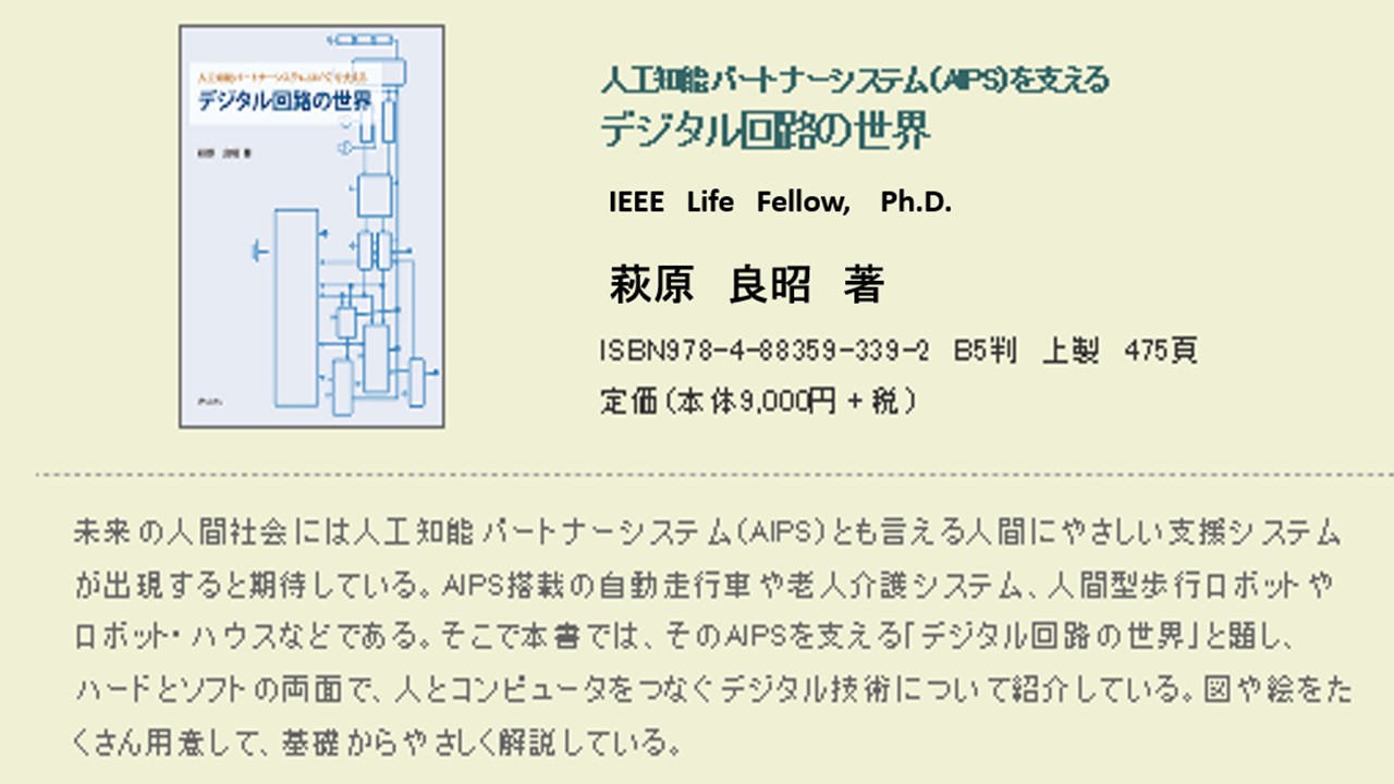
If you are interestied in the book, Please visit
https://www.seizansha.co.jp/ISBN/ISBN978-4-88359-339-2.html
https://www.seizansha.co.jp/
*****************************
理解度アップの基本復習問題
*****************************
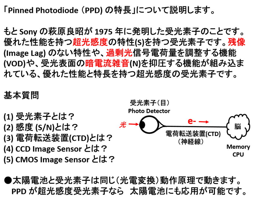
●受光素子とは何か?
●電荷転送装置とは?
●感度とは?
●CCD Image Sensor とは?
●CMOS Image Sensor とは?
*****************************
< Pinned Photodiodeの発明に関係する重要特許出願 >
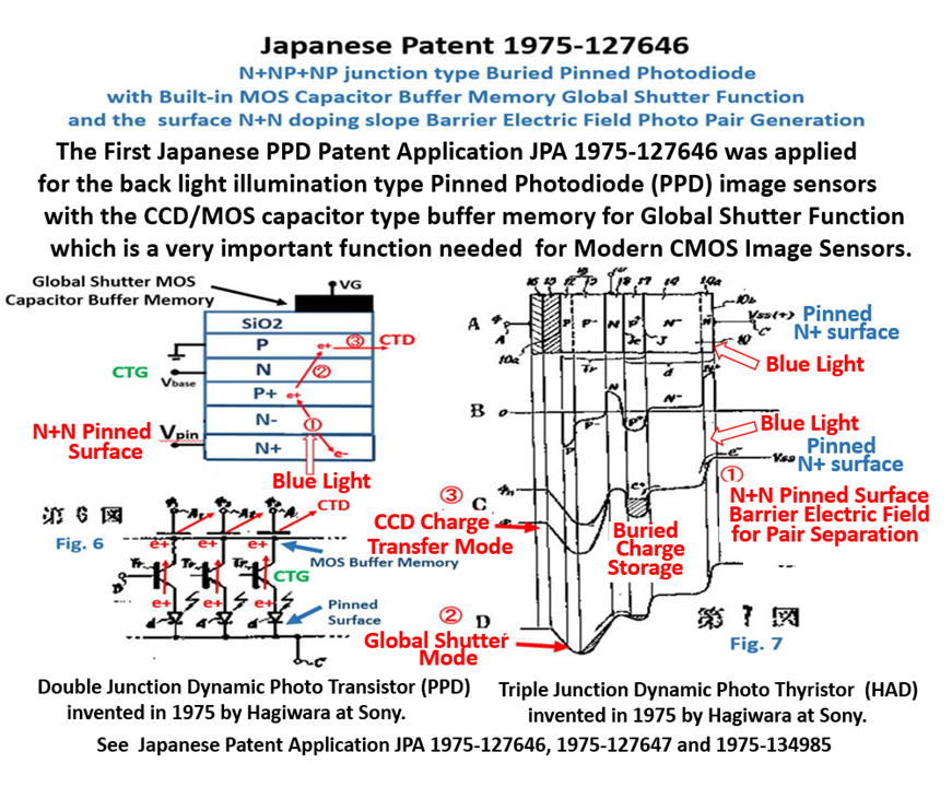
JP1975-127646.pdf
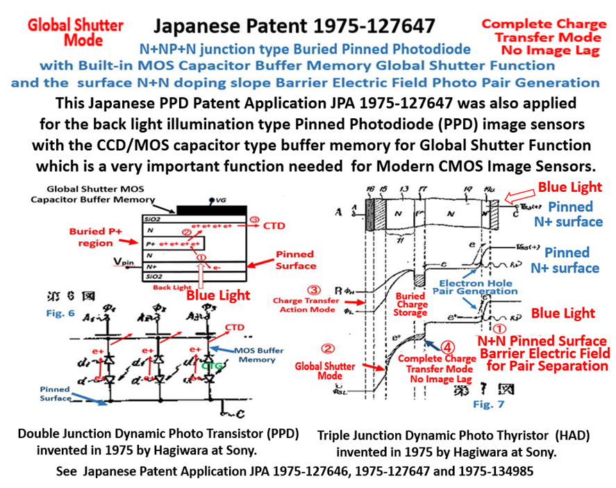
JP1975-127647.pdf
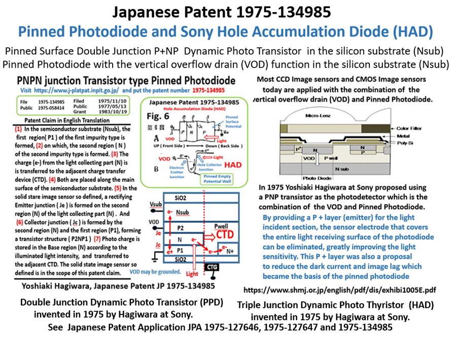
JP1975-134985.pdf
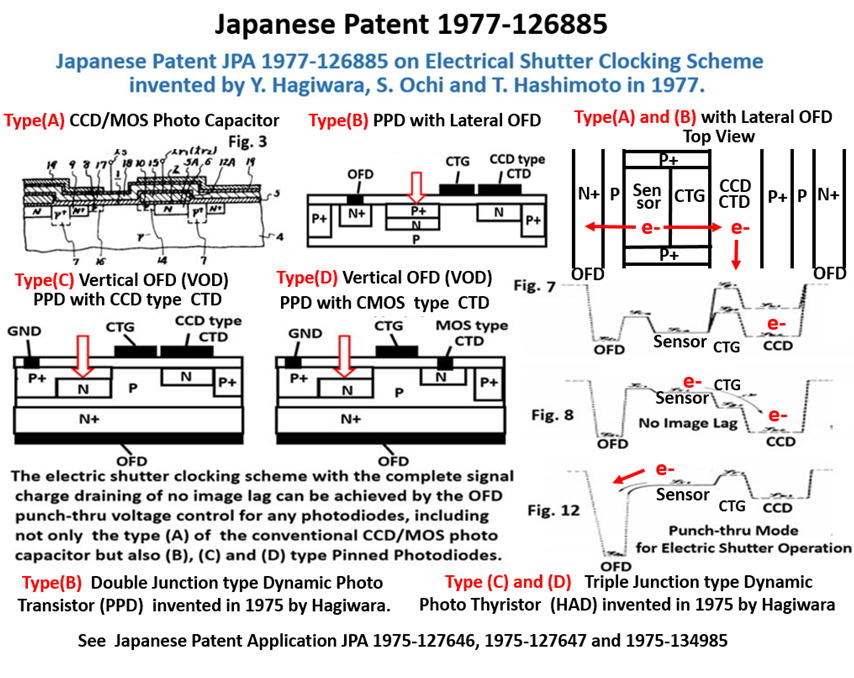
JP1977-126885.pdf
< Pinned Photodiodeの開発に関係する重要学会論文 >
P1978_Pinned_Photodiode_1978_Paper_by_Hagiwara.pdf
P1979_CCD79_in_Edinbourgh_1979.pdf
P1989_SONY_4MSRAM_1989.pdf
P1996_Pinned_Photodidoe_used_in_Sony_1980_FT_CCD_Image_Sensor.pdf
P2001_ESSCIRC2001.pdf
P2008_ESSCIRC2008Hagiwara.pdf
P2013_ISSCC2013PanelTalk.pdf
P2019_3DIC2019Paper_on_3D_Pinned_Photodiode.pdf
P2020_EDTM2020_PaperID_3C4_by_Hagiwara.pdf
P2020_Pinned_Photodiode_Solar_Cell_1.pdf
P2020_Pinned_Photodiode_Solar_Cell_2.pdf
The problem is that very few people understand the difference
between Pinned Photodiode and Buried Photodiode.
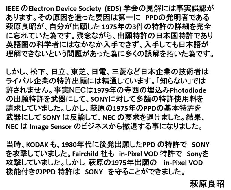
NEC also was attacking SONY HAD (PPD) patent but not successful.
Eventually NEC gave up Image Sensor Business.
Hagwiwara and his friends helped defending Sony against the NEC Patent
Attack.
*******************************************
Image Sensor の発明と開発背景に関する参考文献
*******************************************
*******************************************
●Active in-Pixel MOS Image Sensor
*******************************************
発明(1968)
+++++++++++++++++++++++++++++++++++++++++++++++++++++++++++++++
Peter J. W. Noble,
IEEE Transaction of Electron Devices, 15-4, pp.202-209, (1968)
+++++++++++++++++++++++++++++++++++++++++++++++++++++++++++++++
開発報告(1990)
+++++++++++++++++++++++++++++++++++++++++++++++++++++++++++++++
Fumihiko Andoh, Kazuhisa Taketoshi, Junichi Yamazaki,
Masayuki Sugawara,
Yoshi hiro Fujita, Kohji Mitani, Yukio Matuzawa,
Kenji Miyata, Shuichi Araki,
"A 25 0,000-Pixel Image Sensor with FET Amplification
at Each Pixel for High-Speed Television Cameras",
ISSCC Digest of Technical Papers, pp. 212-213,298, February 1990.
+++++++++++++++++++++++++++++++++++++++++++++++++++++++++++++++
*******************************************
●CCD Image Sensor
*******************************************
発明(1970)と開発報告(1970)
+++++++++++++++++++++++++++++++++++++++++++++++++++++++++++++++
W.S.Boyle and G.E. Smith,
Bell System Technical Journal, 49, pp.587-593(1970)
+++++++++++++++++++++++++++++++++++++++++++++++++++++++++++++++
*******************************************
●低雑音化 CDS 回路
*******************************************
+++++++++++++++++++++++++++++++++++++++++++++++++++++++++++++++
発明(1974)と開発報告(1974)
+++++++++++++++++++++++++++++++++++++++++++++++++++++++++++++++
M.H.White, D.R.Lanpe, F.C.Blaha and I.A.MAck,
"Characterization of Surface Channel CCD Image Arrays at Low Light Level.
IEEE Journal of Solid State Circuits, SC-9, pp.1-13 (1974)
+++++++++++++++++++++++++++++++++++++++++++++++++++++++++++++++
*******************************************
●超光感度・低暗電流雑音・残像のない Pinned Photodiode
*******************************************
発明(1975)
+++++++++++++++++++++++++++++++++++++++++++++++++++++++++++++++
Japanese Patent Applications 1975-127646, 1975-127647,
and 1975-134985 invented by Y.Hagiwara
+++++++++++++++++++++++++++++++++++++++++++++++++++++++++++++++
開発報告(1978)
+++++++++++++++++++++++++++++++++++++++++++++++++++++++++++++++
Y. Hagiwara, M. Abe, and C. Okada,
“A 380H x 488V CCD imager with narrow channel transfer gates",
Proc. The 10th Conference on Solid State Devices, Tokyo, (1978):
Japanese Journal of Applied Physics, vol. 18, Supplements 18-1,
pp. 335-340, (1979)
+++++++++++++++++++++++++++++++++++++++++++++++++++++++++++++++
*******************************************
●アクションカメラ用の電子シャッター機能
*******************************************
発明(1977)
+++++++++++++++++++++++++++++++++++++++++++++++++++++++++++++++
Japanese Patent Application 1977-126885
invented by Y. Hagiwara, S. Ochi and T. Hashimoto.
+++++++++++++++++++++++++++++++++++++++++++++++++++++++++++++++
開発報告(1987)
+++++++++++++++++++++++++++++++++++++++++++++++++++++++++++++++
浜崎正治、鈴木智行、賀川能明、石川貴久枝、宮田克郎、神戸秀夫、
“可変速電子シャタ付IT-CCD撮像素子”、
テレビジョン学会技術報告、vol. 12, no. 12, pp. 31-36, (1988)
+++++++++++++++++++++++++++++++++++++++++++++++++++++++++++++++
*****************************
参考技術書のご紹介
*****************************
「イメージセンサーの本質と基礎」
黒田隆男 著
コロナ社 A5版 199頁
ISBN978-4-339-00845-6
「固体撮像素子の基礎」
安藤隆男・菰淵寛仁 共著
日本理工出版会 A5版 上製 246頁
ISBN4-89019-193-3
「CCD/CMOS イメージ・センサの基礎と応用」
米本和也 著
CQ出版社 A5版 271頁
ISBN4-7898-3626-6
「CCD/CMOS カメラの原理と実践」
安藤幸司 著
オーム社 A5版 214頁
ISBN978-4-274-06851-5
人工知能パートナーシステム(AIPS)を支える
「デジタル回路の世界」
萩原良昭 著
青山社 B5版 上製 475頁
ISBN978-4-88359-339-2
*****************************
Future_of_Image_Sensors_and_Solar_Cells .pdf
Future_of_Image_Sensors_and_Solar_Cells.html
*************************************************************
(1a) Introduction of SSIS Education Committee Program by Chairman 2020/11/25E
(1b) Introduction of SSIS Education Committee Program by Chairman 2020/11/26G
(1c) Introduction of SSIS Education Committee Program by Chairman 2020/11/30B
https://www.ssis.or.jp/en/index.html
SSIS_Education_Activity ( Members Only ) /index.html
*************************************************************
*************************************************************
(2a) P2020_EDTM2020_PaperID_3C4_by_Hagiwara_2020/03/16
on Simulation and Device Characterization of the P+PN+P Junction Type
(2b) Pinned Photodiode and Schottky Barrier Photodiode with Slide Text (PDF)
(2c) EDTM2020_Pinned Photodiode and Schottky Barrier Photodiode with Slide Audio
(html)
*************************************************************
*************************************************************
(3) P2019_3DIC2019_Paper_on_3D_Pinned_Photodiode by Hagiwara 2019
*************************************************************
*******************************************************
(4) Original Japanese Patent Applications on Pinned Photodiode
*******************************************************
JPA1975-127646_on_Triple_Junction_Pinned_Photodiode_with_Global_Shutter_Function.pdf
JPA1975-127647_on_Double_Junction_Pinned_Photodiode_with_Global_Shutter_Function.pdf
JPA_1975_134985/index.html
JP1975-134985_on_Pinned_Photodiode_with_VOD_and_Electric_Shutter_Function.pdf
JPA1977-126885_on_Electric_Shutter_Clocking_Scheme_for _Pinned_Photodiode.pdf
JPA2014-135497_Digital_Transformation_Circuit_for_Image_Sensors.pdf
JPA2020_131313_on_Doubel_Junction_Pinned_Photodiode_Solar_Cell.pdf
History_of_Innovations_in_CMOS_Image_Sensors_edited_by_Hagiwara.pdf
*******************************************************
*******************************************************
(5) Who invented Pinned Photodiode ?.
Hagiwara_Yoshiaki_talks_about_his_1975_inventions_of
Pinned_Phtodiode_in_Japanese_2020_12_06
*******************************************************
*******************************************************
(6) Past Homepages of http://www.aiplab.com