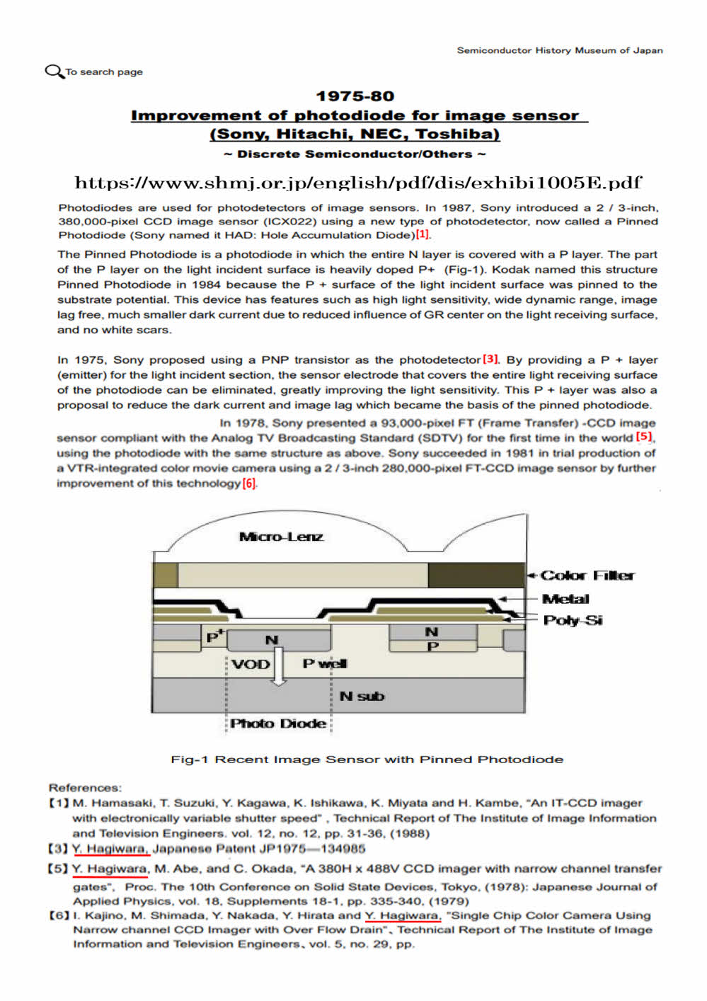
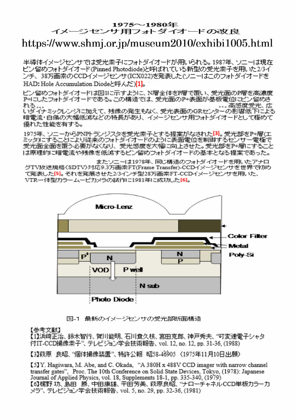
***************************************************
電子Shutter 機能は実は完全に残像のない受光素子でないと
実現不可能です。この事は世間一般には理解されていません。
***************************************************
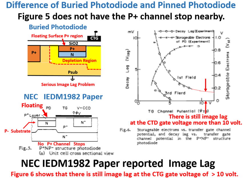
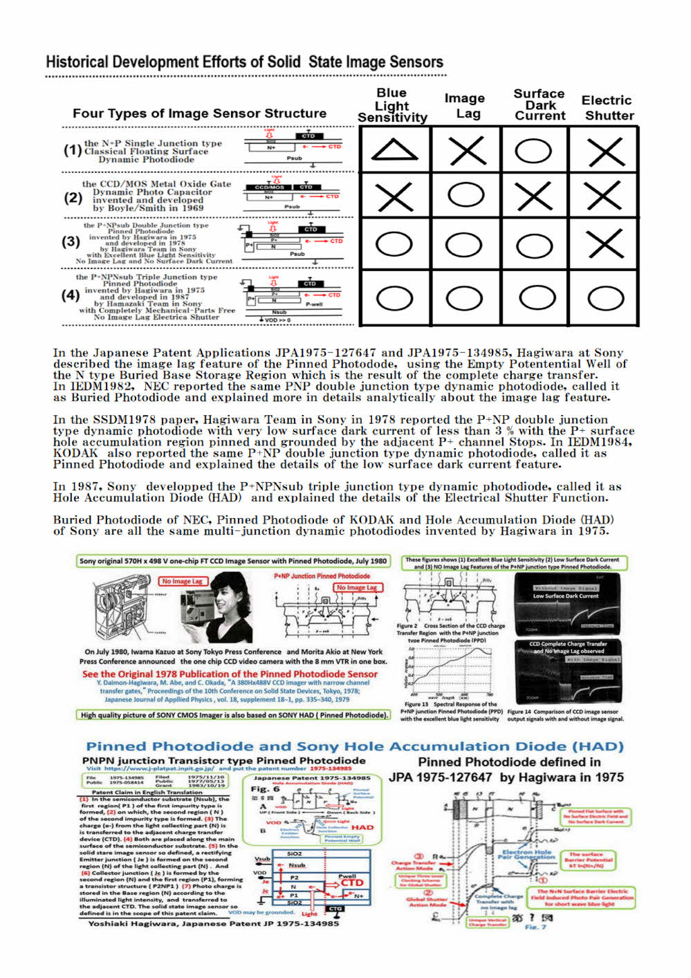
IEDM1982のNECの論文には残像が報告されています。
これはPPDではありませんでした。
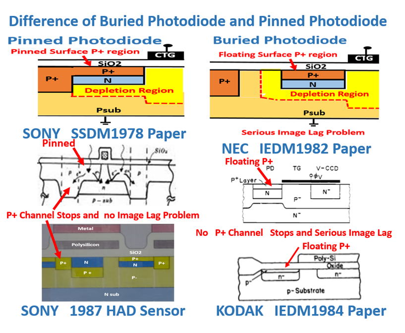
NECの1982年発表の受光素子は、実際は受光面が完全に電圧が
固定、ピン止めできていない、単純にPNP接合型の埋込み型の
Photodiodeに過ぎず、Pinned Photodiodeではありませんでした。
NECやKODAKなど、SONY以外は、おおむね全社、素子間分離に
デジタル MOS プロセス で使う、通常の LOCOS を使っており、
結晶欠陥が多発し、白点や暗電流の問題が多発して、量産性が
乏しいでした。一方、運よく、SONYは CCD独自プロセスを考案し、
他社が通常採用している LOCOS を SONY は採用しませんでした。
KODAK の1984年発表の受光素子も、実際は受光面が完全に電圧が
固定、ピン止めできていない、単純にPNP接合型の埋込み型の
Photodiodeに過ぎず、Pinned Photodiodeではありませんでした。
LOCOSを使うと、埋込みN層が、受光部のP+層と、LOCOSのP+領域
を分断する様子が実際の他社の受光素子断面図から読み取れます。
この事実を NEC も KODAK も一般の技術者も理解していなかった様です??
![]()
また、FOSSUMの 2014年の論文は 不当にも 「萩原の1975年特許には
残像がない事を示す記載がない」と攻撃しました。これは事実無根の攻撃です。
萩原の1975年の3つの特許には、埋込み電荷蓄積層から電荷転送部への、
完全電荷転送を示す、Empty Potential Well の電位図が明示されています。
*******************************************************************
Hagiwara did invent the virtual phase charge tarnsfer mode
for the three phase charge transfer operation with the two CCD MOS gates.
*******************************************************************
![]()
![]()
![]()
![]()
![]()
![]()
![]()
![]()
As shown above, Hagiwara indeed invented the virtual phase charge transfer
operation mode using the completely image lag free Pinned Photodiode,
in the two gate MOS capacitor charge transfer clocking scheme as shown
above.
Fossum 2014 is insulting SONY and Hagiwara
by making incorrect and false statements.
Fossum 2014 paper is incorrect, false and fake.
![]()
*******************************************************************
次のWEB投稿者も、「萩原が Pinned Photodiode の発明者だ」と明言しています。
「もとNECの寺西さんを間違ってPinned Photodiodeの発明者として過大評価した」と明記しています。
https://electronics.stackexchange.com/questions/83018/difference-between-buried-photodiode-and-pinned-photodiode
また、SONYも、「萩原が Pinned Photodiode の発明者だ」と明言しています。
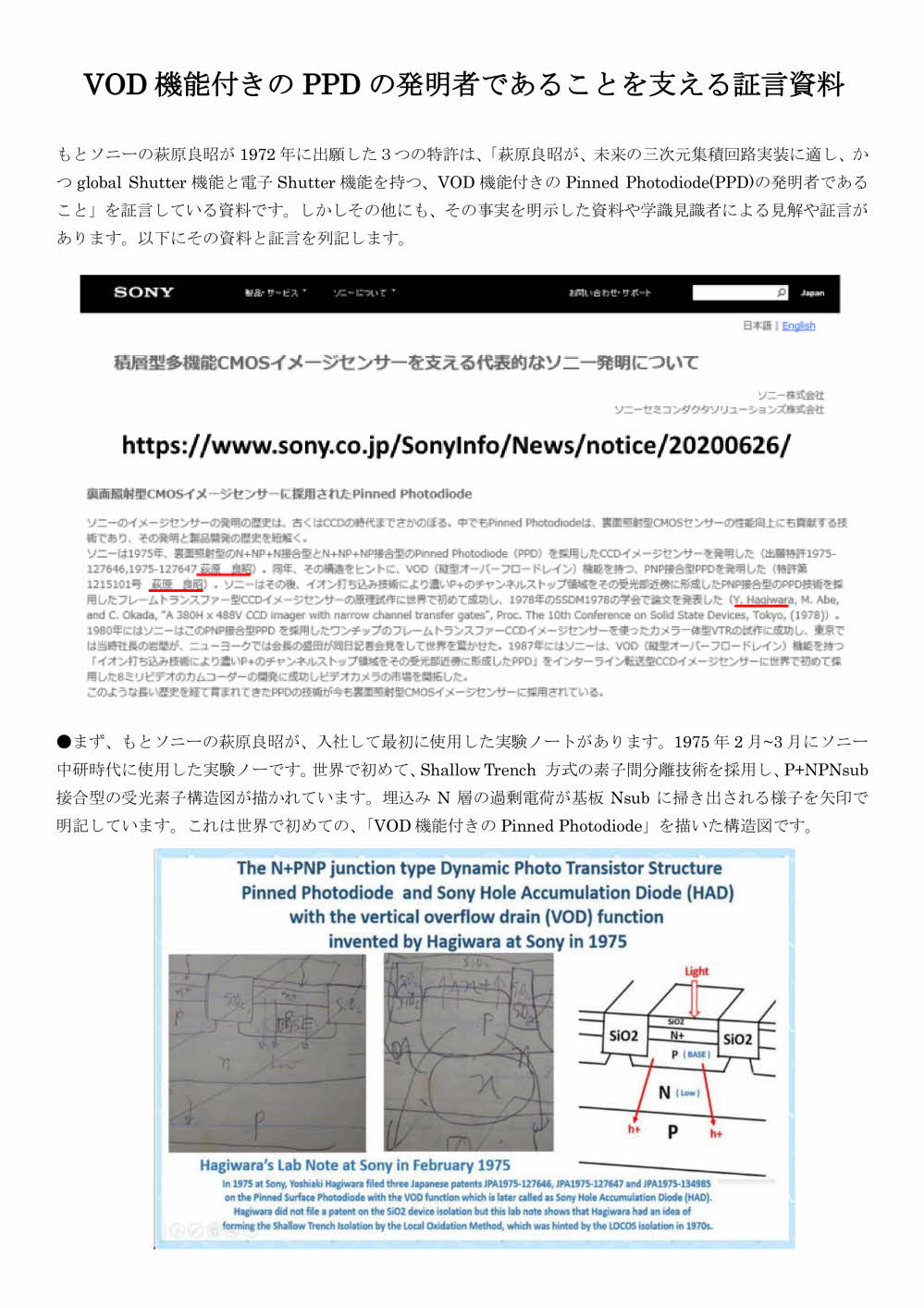
また、半導体産業人協会の日本歴史館の公式WEB掲載でも、
「萩原が Pinned Photodiode の発明者だ」と明言しています。
NECの1980年寺西特許の PNP接合埋め込みPhotodiodeの特許は無効です。
もとSONYの萩原が既に1975年に、埋込み型でかつ、
受光面がピン止めされた、
残像のない特性を持つ、P+NPNsub接合型Pinned Photodiodeを発明しています。
東芝の1978年山田特許の N+PN接合のVOD特許も無効です。
もとSONYの萩原が既に1975年に、VOD付きの残像のない特性
を持つ、P+NPNsub接合型Pinned Photodiodeを発明しています。
残像のない特性を持つ、P+NPNsub接合型Pinned Photodiode だけが、
高速アクション撮影を可能にする、電子 shutter 機能が可能となります。
東芝の1978年山田特許の N+PN接合の表面のN+電荷蓄積部は
Floating 状態ですので、残像があり、これでは、完全に信号電荷を
抜き取れないので、これでは 電子 Shutter 機能は実現不可能です。
*********************************************************************
http://www.aiplab.com/index_Page003_Invention_of_Pinned_Photodiode_in_1975.html
*********************************************************************
Yoshiaki Hagiwara wrote a book on
"the World of Artificial Intelligent Digital Circuits",
which is important and needed to built
the intelligent image sensor systems.
ISBM978-4-88359-339-2
Hard Cover, 460 page,
\ 9000 Japanese Yen + tax
If you are interestied in the book, Please visit
https://www.seizansha.co.jp/ISBN/ISBN978-4-88359-339-2.html
https://www.seizasha.co.jp/
*************************************************************
The following four Japanese Patent Applications explained that
Hagiwara invented Pinned Photodiode with VOD function in 1975.
index001_Image_Sensor_1975_1977_and_2014_Patents.html
*************************************************************
index002_Facts_on_Invention_of_Pinned_Photodiode.html
index003_Hagiwara_Publication_List.html
index004_My_Wonderful_Memory_Pictures.html
index005_Image_Sensor_Story_by_Hagiwara.html
*************************************************************
********************************************************
hagiwara-yoshiaki@aiplab.com http://www.aiplab.com/
hagiwara@ssis.or.jp http://www.ssis.or.jp/en/index.html
********************************************************
******************************
Return to Top Page
http://www.aiplab.com/
*********************************