

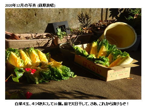
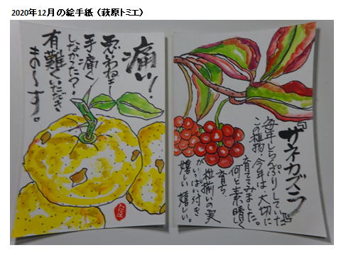

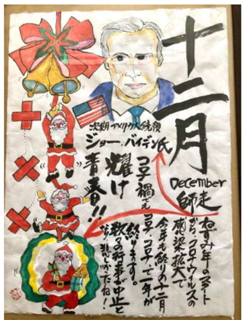

***********************************************
******
豆知識 <-- 萩原良昭が知らなかった言葉です(苦笑)。
******
岳樺(ダケカンバ)
木犀(もくせい)
曼珠沙華(マンジュシャゲ)
欅(ケヤキ)
凭れる(もたれる)
繁(しげ)
諍(いさか)う
言争(いいあらがう)
ひぐらし
ユキノシタ(雪の下)の花言葉とは?
切岸(きりぎし)とは?
莪 とは ?
蓼莪之詩 (りくがのし) とは ?
梢(こずえ) とは?
*************************************
●ハングルの勉強をしています。
*************************************
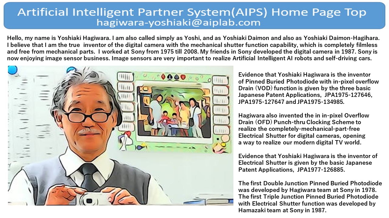
●まず、日本を代表する技術集団の半導体産業人協会は、「世界ではじめて、
Double 接合の P+NP junction型 Dynamic Photo Transistor( 後に学会で
Pinned Photodiodeと呼ばれる、超光感度の光電変換素子)を、もと Sony の
萩原良昭が 1975年に既に提案し、1978年にはその開発に成功していた。」
という事実を半導体産業人協会は日本半導体歴史館の公式WEB掲示公開した。
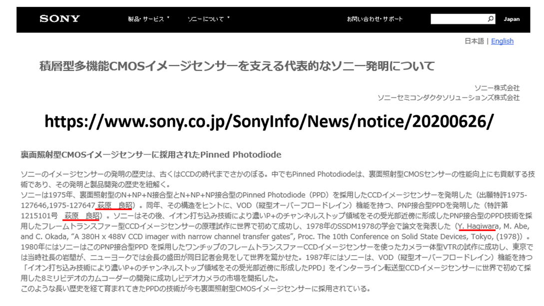
●また、世界を代表する電子電気産業の国際企業である技術のSONYも、
「萩原良昭が、世界で初めて、Double 接合の P+NP junction型である、
Dynamic Photo Transistor構造の Pinned Photodiodeと、VOD 機能
と電子 Shutter 機能を持つ、Triple 接合の P+NPNsub Junction型 の
Dynamic Photo Thyristor 構造である Pinned Photodiode、別名、
Sony の Hole Accumulation Diode (HAD) の発明者である事を Sony
の公式 WEB サイト に 今回初めて 開示、掲示公開した。
その公開が遅れた 理由は、
1990年から2000年まで、長期に渡る Fairchild 社と SONY 間で熾烈な
特許戦争が水面下で生じたためである。その詳細は 公開されること
はなかったが、SONYが最終的に2000年に勝利した。
また、NEC や KODAK とも水面下で長い特許戦争が継続した為である。
NECは、寺西氏の1979年出願特許を武器に SONY に多額の特許使用料
を請求したが、SONY の萩原の 1975年 の Pinned Photodiode の基本特許
を武器にして、SONY は、NECの要求をはねのけた。その結果、NECは
最終的に Image Sensor の市場から撤退することになった。
一方の KODAK は、SONYと技術提携を結び、共存の道を選んだ。
************************************
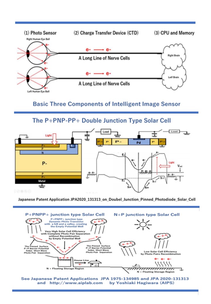
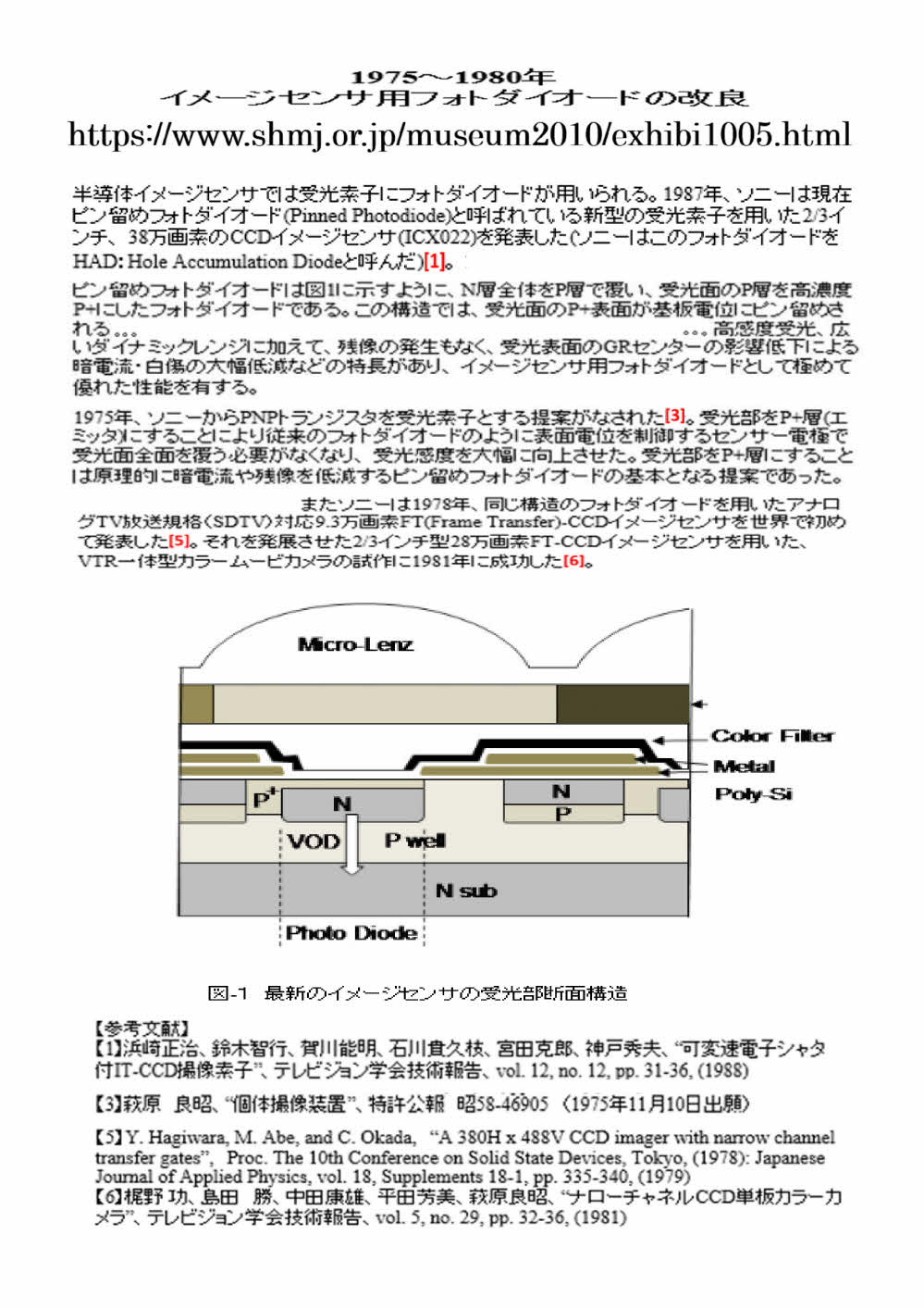
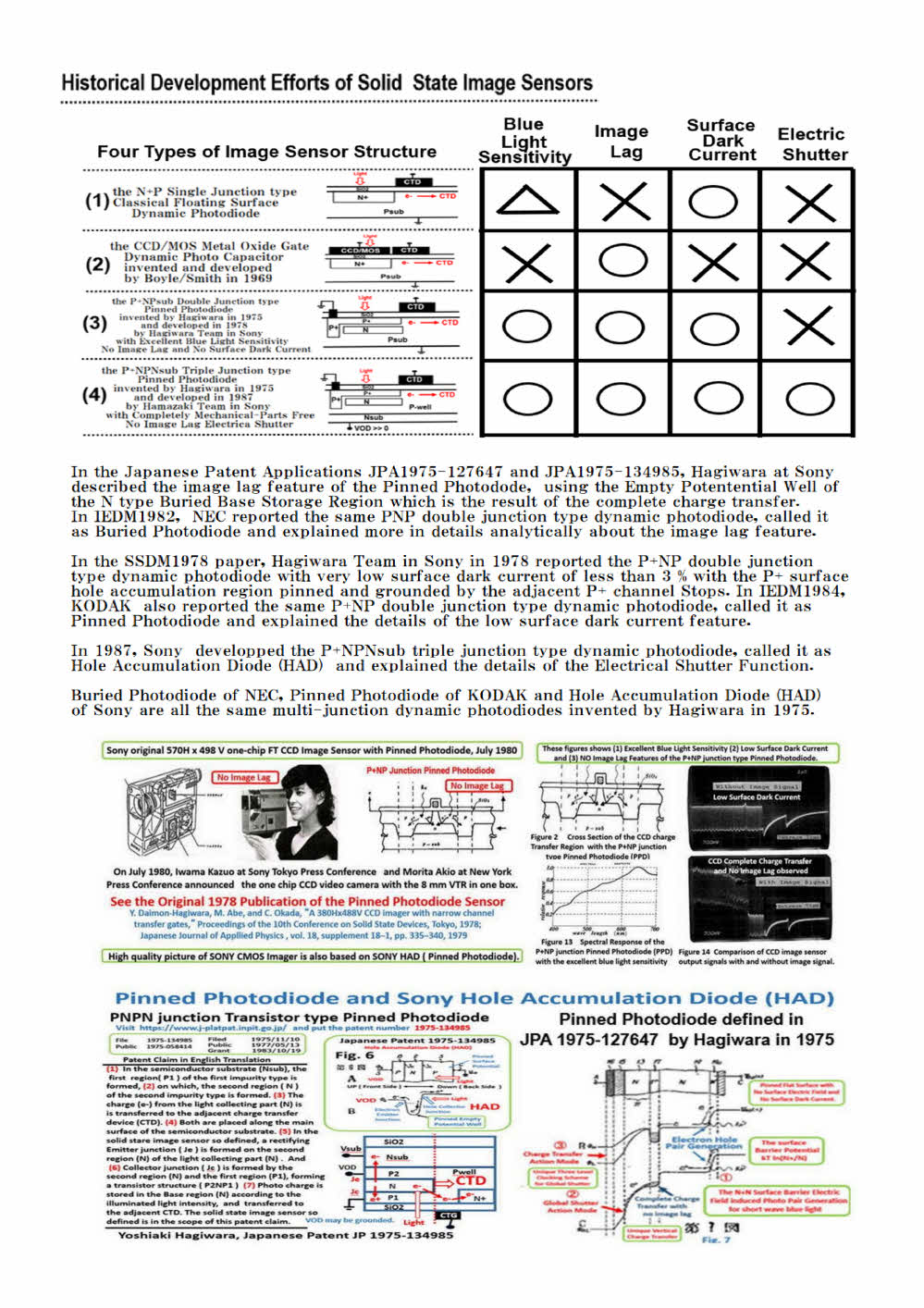
もと Sony の萩原は、1975年に Double 接合型の Dynamic Photo Transistor を発明した。
************************************
(1)短波長青色感度特性に優れ、(2)表面がピン留めされており、表面暗電流少なく、また
(3) 完全電荷転送により残像のない映像を実現した。さらに(4)過剰信号電を垂直基板
方向に調整し流し出す、Vertical Overflow Drain (VOD) 機能を実現した。
************************************
また萩原は
1975年、同時に 垂直 Punch thru Mode での完全電荷転送
を特徴とする、Triple 接合型の Dynamic PhotoThyristor を発明した。
************************************
完全に Filmless で Mechanical 部品不要の電子 shutter 機能を
実現し、Film 映像社会から、電子映像社会の実現に貢献した。
************************************
●だれが見ても上記2つの WEB掲載と下記の発明協会の記載には完全なる
矛盾があることが理解できます。さて、どちらが真実でしょうか?発明協会は
真実を社会に伝える義務があるはずですが、何かここに矛盾を感じます???
************************************
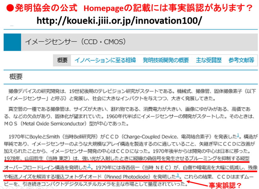
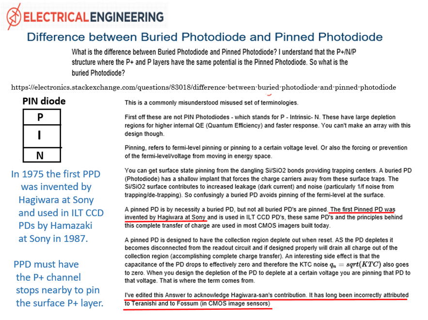
発明協会のWEB掲載には 1979年に寺西信一が 埋込みPhotodiode ( Pinned
Photodiode ) の発明者と断定ているが、これは明らかに事実誤認である。すでに
萩原が3件の1975年特許出願が証拠で、埋込み Photodiode と Pinned Photodiode
を萩原は発明している。また IEDM1982のNECの論文は、先行者の仕事を正当に
引用しない論文であった。その論文の埋込み Photodiode には残像が報告されている。
これは明らかに Pinned Photodiode の基本条件を満足しない。 IEDM1982のNEC
の論文は Pinned Photodiode の論文ではない。その事実関係も理解されていない。
もと SONYの萩原良昭が真のVOD 付き Pinned Photodiode の
発明者である事は、以下の3件の 1975 年出願特許と、1977 年
の電子 shutter の clock 駆動方式の特許と、1978年に 国際学会
SSDM1978 で発表した論文がその証拠である。
http://www.aiplab.com/JP1975-127646.pdf
http://www.aiplab.com/JP1975-127647.pdf
http://www.aiplab.com/JP1975-134985.pdf
http://www.aiplab.com/JP1977-126885.pdf
http://www.aiplab.com/P1978_Pinned_Photodiode_1978_Paper_by_Hagiwara.pdf
また、萩原が Pinned Photodiodeの本当の発明者である事を、
1975年の特許(発明)と1978年の論文(開発)を証拠に明確に
解説した IEEE の国際学会で論文が2件連続投稿受理され、
国際社会の舞台で発表できた事は非常に喜ばしい限りである。
(1) P2019_3DIC2019Paper_on_3D_Pinned_Photodiode.pdf
(2) P2020_EDTM2020_PaperID_3C4_by_Hagiwara.pdf
Slide_Audio...P2020_EDTM2020_PaperID_3C4_Slide_Audio_by_Hagiwara(html)
Slide_Text.... P2020_EDTM2020_PaperID_3C4_Slide_Text_by_Hagiwara(pdf)
2020年11月13日(金)の産業タイムズ社の
電子デバイス新聞(電子版)には萩原良昭
の人物紹介の取材記事が掲載されました。
https://www.sangyo-times.jp/article.aspx?ID=5331
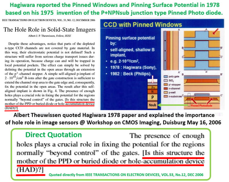
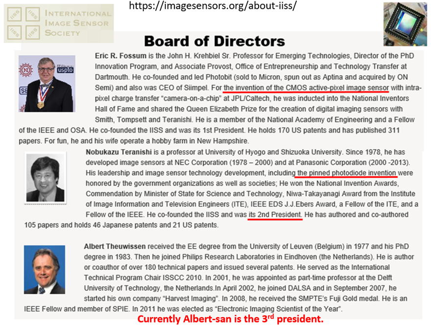
また、今の International Image Sensors Society (IISS)の
会長で世界の Image Sensorの代表的な権威ある科学者
で Delft 大学の Prof. Albert Theuwissen は、2006年の
学会論文の中で、萩原が原理試作に成功し、SSDM1978
の国際学会でその開発成果を報告したのを引用して、
「萩原の1978年開発した P+NP のDouble 接合型の受光
素子が、NECの埋込み Photodiode、KODAK の Pinned
Photodiode、および、SONYの Hole Accumulation Diode
(HAD) の Mother ( 生みの親 = 発明者 )だと賞賛した。
偉大な開発者を「育ての親」と呼び、英語で Father と
表現するのに対して、偉大な発明者を「生みの親」と呼び、
英語で Mother と表現されることを理解していただきたい
です。この論文は、萩原が Pinned Photodiodeの発明者
である事を明らかにした、数少ないが重要な論文です。
また、下記 技術教育のWEB投稿サイトでも匿名ですが、
ここでも 「萩原が Pinned Photodiodeの発明者である」
とコメントする内容を投稿した方がおられます。
寺西さんと Fossum は間違って過大評価されていると
きびしく指摘した投稿サイトの内容です。この人は、真実
をWEB投稿の中で指摘しています。現在、孤軍奮闘する
萩原にとっては大変数少ない貴重な励みになるものです。

![]()
A Fake Review of the Pinned Photodide by Eric Fossum
Many people said, "This is a misleading, doubtful and fake paper.",
which did not quote properly many important reference papers such
as the acive pixel amp circuit by Peter Noble 1968 invention, and
the patent applications such as JPA 1975-127646, 1975-127647
and 1975-134985 filed in 1975 by Yoshiaki Hagiwara at Sony.
In these basic Japanese 1975 Patent Applicaitons, Hagiwara drew
for the first time in the Pinned Photodiode structure, the Empty
Potential Well of the important image lag free feature. The Double
Junction type Dynamic Photo Transistor Hagiwara invented in 1975
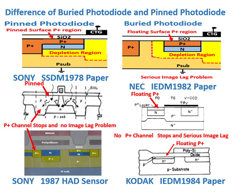
was later called as Pinned Photodiode by KODAK in 1984.
Kodak, not NEC, successfully developped the PPD used in ILT CCD
image sensors in 1984 for the first time in the world.
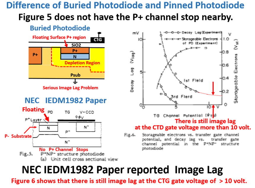
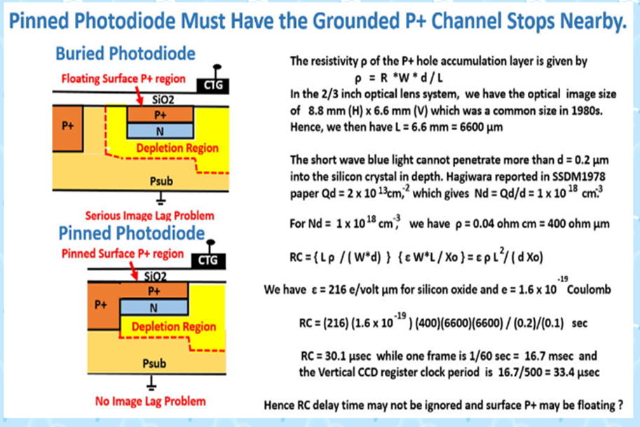
The Buried Photodiode used in the ILT CCD imagers, reproted in
IEDM1982 by NEC Teranishi team, had the image lag property, which
is the evidence that the 1982 NEC Teranishi Photodiode is not a PPD.
Hagiwara also invented in 1975 patent applications theTriple Junction
type Dynamic Photo Thyristor with the Punch-thru Vetical Overflow
Drain (VOD) function, which was later also called by Sony as Hole
Accumulation Diode (HAD) with the Electrical Shutter function.
Albert-san undersood very well that the original PPD invented in 1975
reported in SSDM1978 by Hagiwara was intended for the excellent short
wave blue sensitivity as the top priority feature.
Hagiwara also descibed in 1975 about other important features of
Pinned Photodiode such as the Empty Potential Well of complete
charge transfer operation for the low image lag feature and the
pinned surface P+ hole accumulation with no surface electric
field and with no surface dark current noise.
Albert-san mentioned also that the photodiode Hagiwara reported
in SSDM1978 was indeed a Pinned Photodiode (PPD), which was
originally invented in 1975 and developped also by Hagiwara-team
in 1978 before the Teranshi 1979 patent application of the Buried
Photodiode, which is by neccesity not always a Pinned Photodiode.
The following e-mail communication confirms these facts.
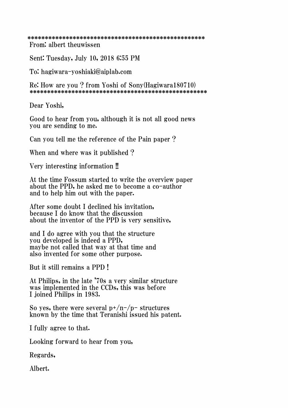
This was just a private e-mail communication between Albert-san
and Hagiwara, but Hagiwara was very happy to hear Albert-san's
very honest words, telling the very truth about the PPD invention.
Albert-san is now the president of
Internationa Image Sensors Society.
https://imagesensors.org/
I see a big contradiction between Albert-san's 2018 commnet
shown above and the IISS official home page description shown
below about Teranish-san's carrier on Pinned Photodiode..
Hagiwara invented PPD in 1975 for the excellent blue sensitivity.
But Hagiwara also explained in the patent applications that PPD
has the low image lag and the pinned P+ hole accumulation layer
with the low surface dark current. Indeed Hagiwara invented PPD.
**********************************
SONY 半導体OB会は、
もとSONYの萩原良昭が
Pinned Photodiodeの
真の発明者である
と断定しています。
**********************************
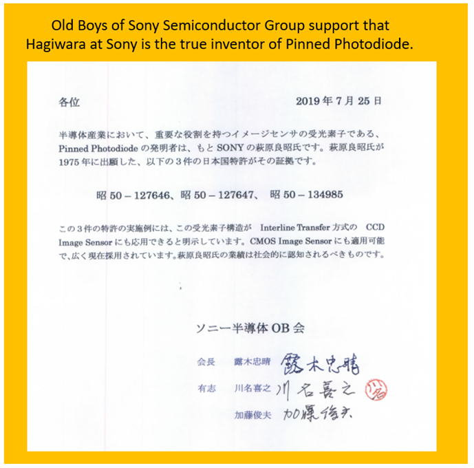
川名喜之さんは、ソニー半導事業本部CCDプロセス開発部を
歴任され、ソニー中央研究所のもと副所長でした。
加藤俊夫さんは、ソニー半導事業本部CCDプロセス開発部門の
もと統括部門長でした。
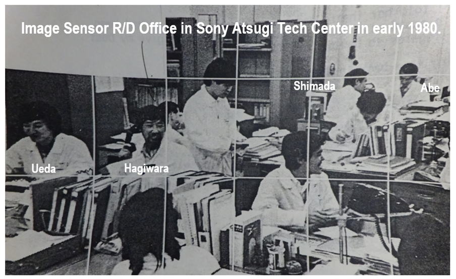
1980年代の当時、露木忠晴先輩や、 加藤俊夫開発部長、
川名喜之開発部門長に守られ、萩原は Image Sensor の
開発部隊の一員として楽しく仕事に励むことができました。
結論として
http://www.aiplab.com/Evidence_that_Hagiwara_is_the_inventor_of_Pinned_Photodiode_in_Japanese.pdf
******************************************
Please visit for the details..... AIPS Library
******************************************
******************************
Return to Top Page
http://www.aiplab.com/
*********************************
**************************************************************
This is AIPS ( aiplab.com ) Homepage
**************************************************************
Jump to Part 001 002 003 004 005 006 007 008 009 010 011 012 013
**************************************************************
*********************************************************************
Please write me freely anything related to my activities: *********************************************************************
hagiwara-yoshiaki@aiplab.com for my activity at http://www.aiplab.com/
hagiwara@ssis.or.jp for my activity at http://www.ssis.or.jp/en/index.html
*********************************************************************