**************************************************************
This is index_2020_12_07_007.html
**************************************************************
Jump to Part 001 002 003 004 005 006 007 008 009 010 011 012 013
**************************************************************
![]()
*****************************************************************
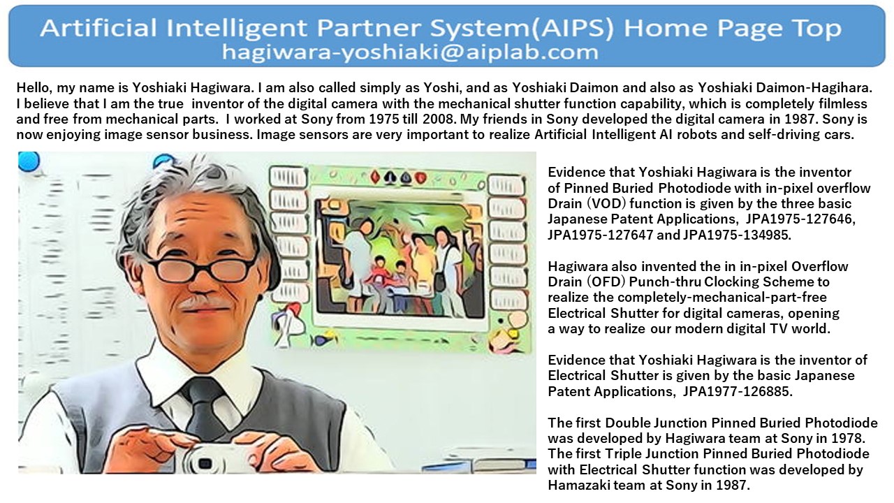
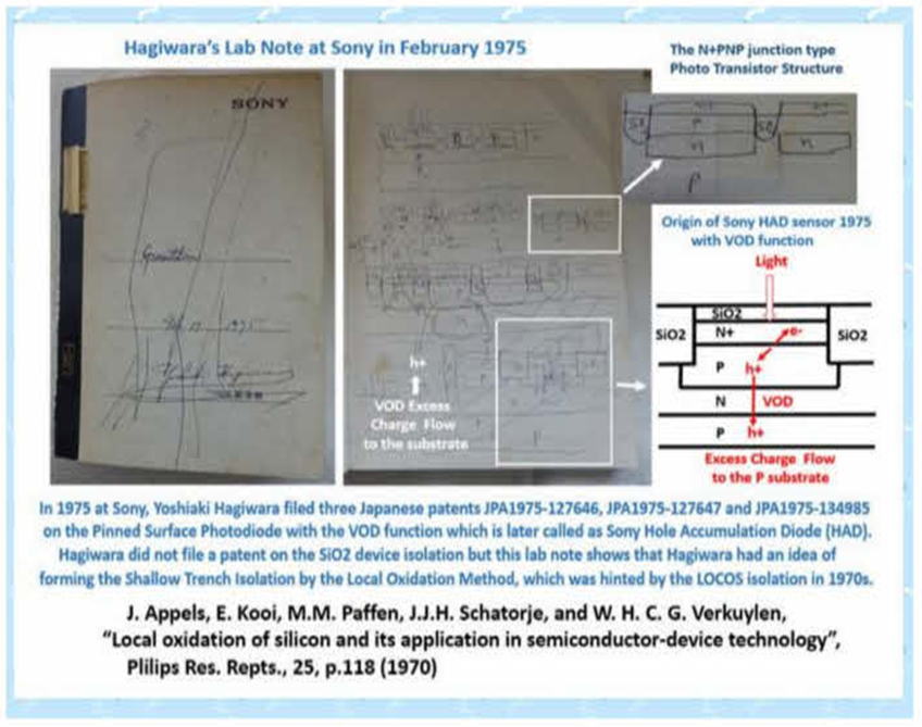
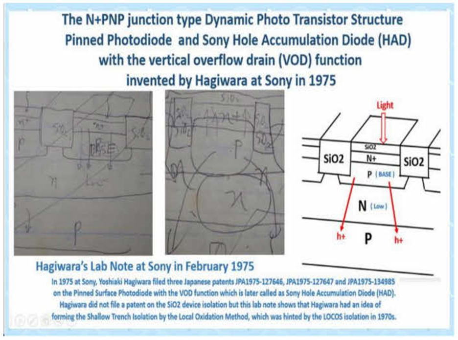
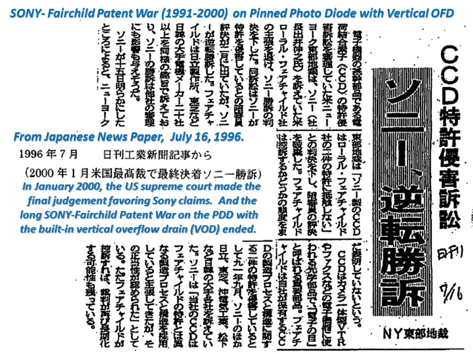
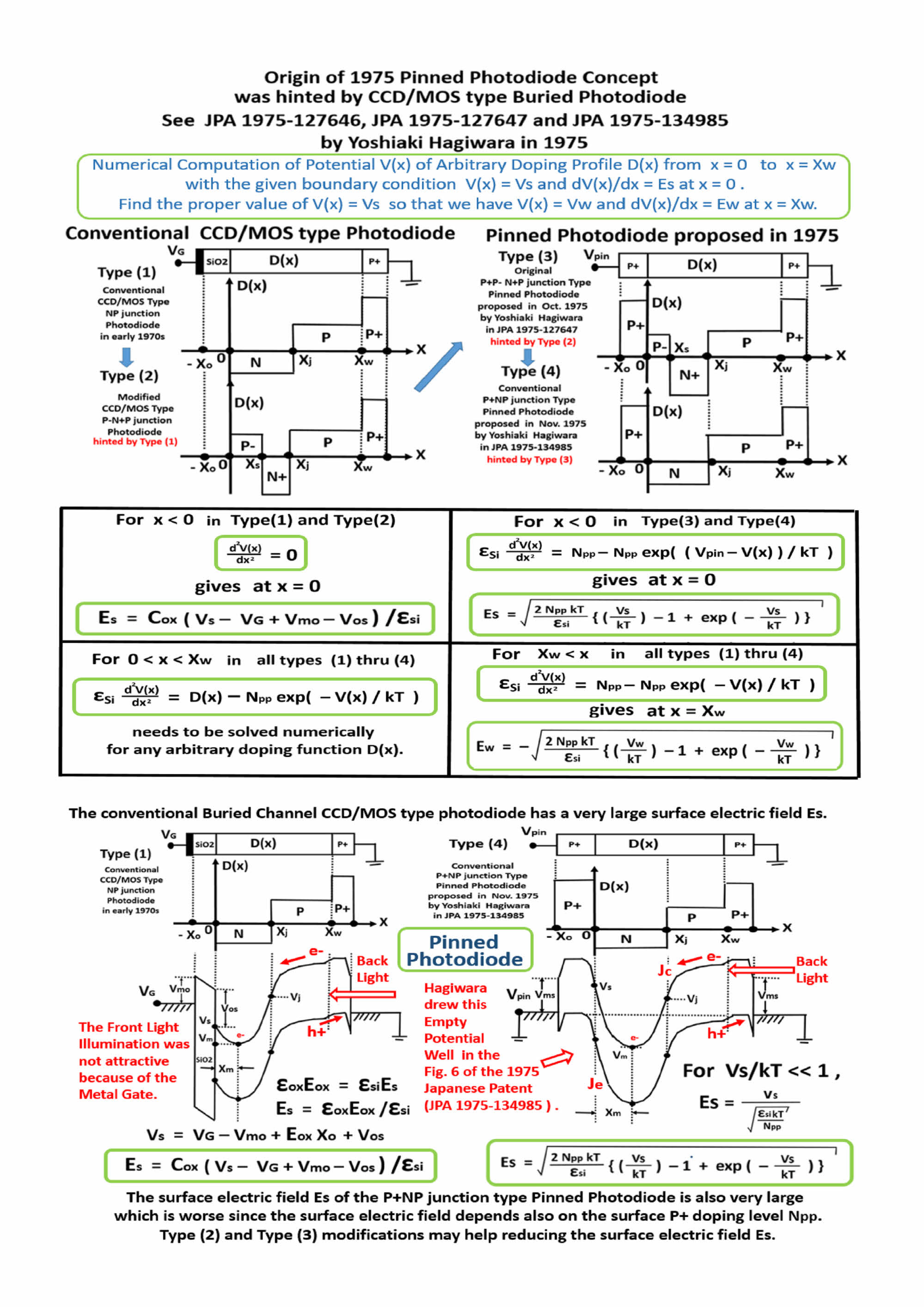
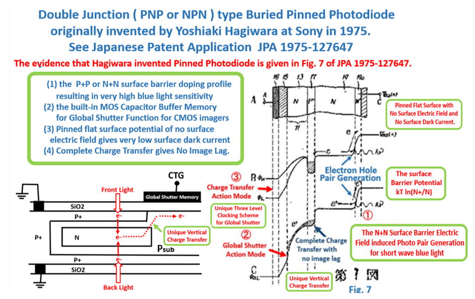
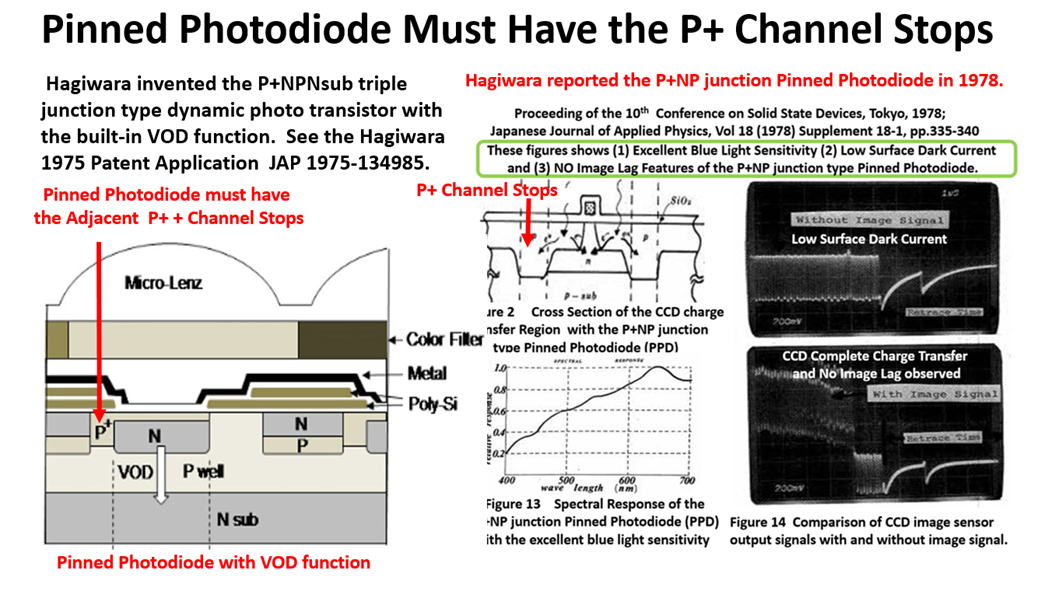
The Evidence that Hagiwara at Sony is the inventer of Pinned Photodiode
is
given by the three 1975 Japanese Patent Applications , JPA 1975-127646,
JPA 1975-127647 and JPA 1975-134985. Details are explained below.
*****************************************************************

Hagiwara is also the inventor of the Global Shutter Function
needed in the modern CMOS Image Sensors. For the details,
please read the conference publication papers:
http://www.aiplab.com/P2019_3DIC2019Paper_on_3D_Pinned_Photodiode.pdf
http://www.aiplab.com/P2020_EDTM2020_PaperID_3C4_by_Hagiwara.pdf
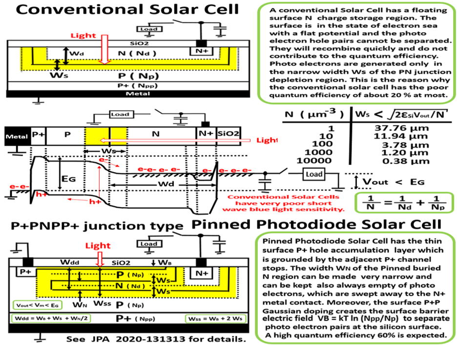
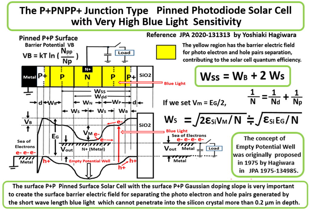
Pinned Photodiode has an excellent short wave blue light sensitivity
that can be also applied to the Pinned Photodiode type Solar Cells.
http://www.aiplab.com/P2020_Pinned_Photodiode_Solar_Cell_1.pdf
http://www.aiplab.com/P2020_Pinned_Photodiode_Solar_Cell_2.pdf
************************************************************
Hagiwara at Sony invented Pinned Photodiode in 1975
index000_Invention_of_Pinned_Photodiode_in_1975.html
index001_Image_Sensor_1975_1977_and_2014_Patents.html
index002_Facts_on_Invention_of_Pinned_Photodiode.html
index003_Hagiwara_Publication_List.html
index004_My_Wonderful_Memory_Pictures.html
index005_Image_Sensor_Story_by_Hagiwara.html
index006_Slide_Sony_Atsugi_Tech_2020_07_10.html
*************************************************************
http://www.aiplab.com/Memo_2020_09_17_by_Yoshiaki_Hagiwara.html
AIPS Library Under Construction Now
*********************************************************************
Please write me freely anything related to my activities:
*********************************************************************
hagiwara-yoshiaki@aiplab.com for my activity at http://www.aiplab.com/
hagiwara@ssis.or.jp for my activity at http://www.ssis.or.jp/en/index.html
*********************************************************************
******************************
Return to Top Page
http://www.aiplab.com/
*********************************
**************************************************************
This is index_2020_12_07_007.html
**************************************************************
Jump to Part 001 002 003 004 005 006 007 008 009 010 011 012 013
**************************************************************