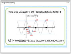
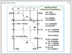
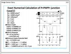
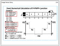
**************************************************************
This is index_2020_12_07_010.html
**************************************************************
Jump to Part 001 002 003 004 005 006 007 008 009 010 011 012 013
**************************************************************
index006_Slide_Sony_Atsugi_Tech_2020_07_10.html
http://www.aiplab.com/Slide_Sony_Atsugi_Tech_2020_07_10_Slide001_to_010.html
http://www.aiplab.com/Slide_Sony_Atsugi_Tech_2020_07_10_Slide011_to_020.html
http://www.aiplab.com/Slide_Sony_Atsugi_Tech_2020_07_10_Slide021_to_030.html
http://www.aiplab.com/Slide_Sony_Atsugi_Tech_2020_07_10_Slide031_to_040.html
http://www.aiplab.com/Slide_Sony_Atsugi_Tech_2020_07_10_Slide041_to_050.html
http://www.aiplab.com/Slide_Sony_Atsugi_Tech_2020_07_10_Slide051_to_060.html
http://www.aiplab.com/Slide_Sony_Atsugi_Tech_2020_07_10_Slide061_to_070.html
http://www.aiplab.com/Slide_Sony_Atsugi_Tech_2020_07_10_Slide071_to_080.html
http://www.aiplab.com/Slide_Sony_Atsugi_Tech_2020_07_10_Slide081_to_090.html
http://www.aiplab.com/Slide_Sony_Atsugi_Tech_2020_07_10_Slide091_to_100.html
http://www.aiplab.com/Slide_Sony_Atsugi_Tech_2020_07_10_Slide101_to_110.html
http://www.aiplab.com/Slide_Sony_Atsugi_Tech_2020_07_10_Slide111_to_119.html
index006_Slide_Sony_Atsugi_Tech_2020_07_10.html
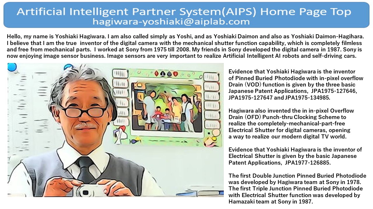
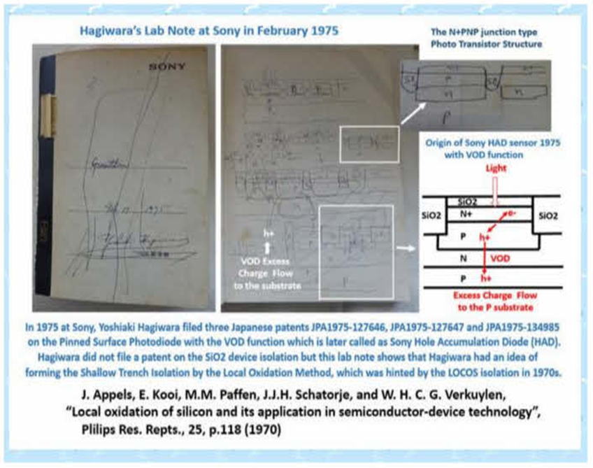
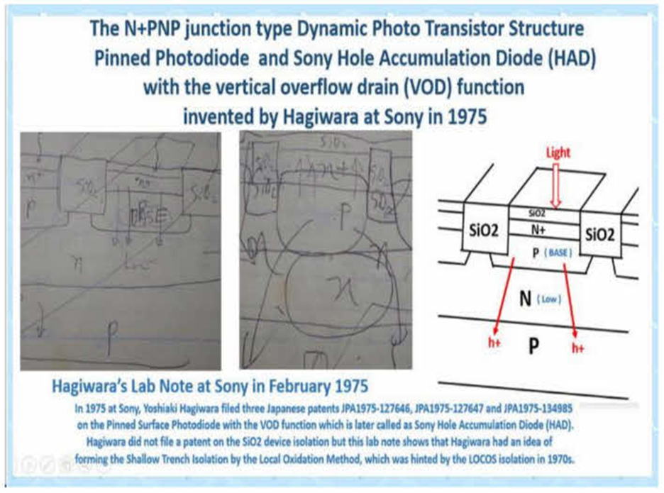
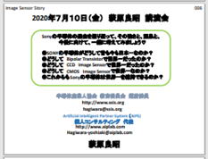
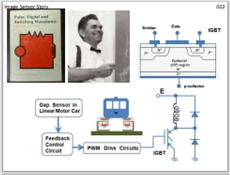
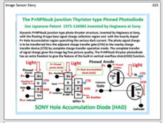
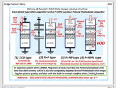
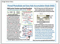
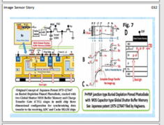
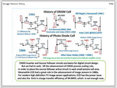
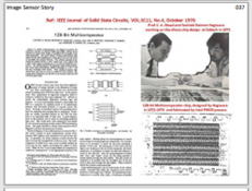
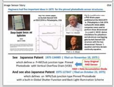
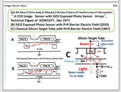
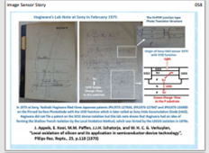
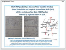
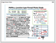
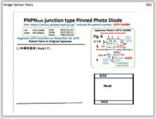
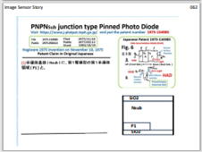
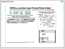
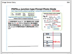
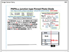
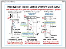
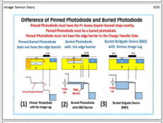
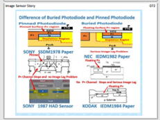
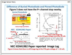
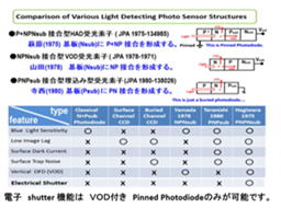
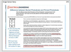
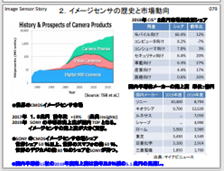
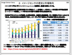
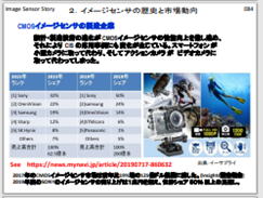
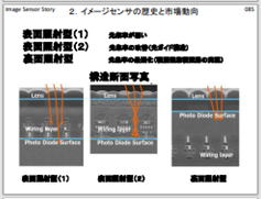
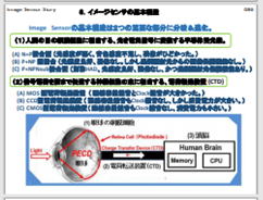
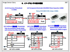
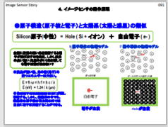
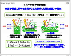
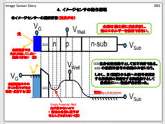
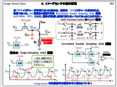
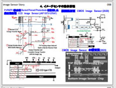
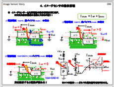
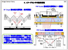
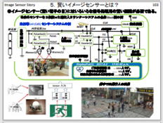
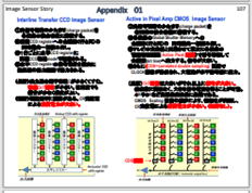
●縦型 Overflow Drain ( VOD ) 機能付きで、かつ残像のない 、
P+NPNsub 接合型の Pinned Photodiode でないと、電子 shutter
機能は実現しません。この 1975 年の萩原のP+NPNsub 接合型の
Dynamic Photo Transistor の発明により、メカ Free の電子 shutter
機能付きのビデオカメラが実現しました。これにより、Film のない、
メカ Free の、電子映像の技術革新社会が実現したと思っています。
http://www.aiplab.com/Memo_2020_08_21_by_Yoshiaki_Hagiwara.html
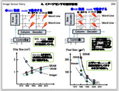
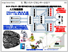
●Intel は、早々と大容量メモリ産業から脱却し、Intelligent Processor
の開発商品化に注力し、大企業に成長しました。これから Sonyも同様、
Intelligent Processor の開発商品化に注力してほしいです。日本の
もの造り産業のお家芸でもある、AI IoT Robitics の実現の為にも、
Multi Chipの3次元集積回路と その実装技術を武器に、日本の半導体
産業を支えてほしいです。世界をもリードして行ってほしいです。
http://www.aiplab.com/Memo_2020_08_23_by_Yoshiaki_Hagiwara.html
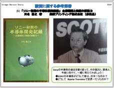
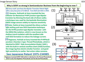
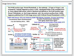
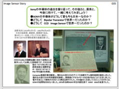
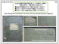
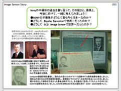
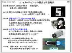
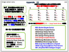
●川名さんと加藤さんのアイデアは特許出願されていませんが
日本の半導体産業を支えた基本特許のアイデアだったと思います。
残像のない、Pinned Photodiode を採用した電子 shutter 機能の発明
はFilm 社会から、メカ Freeの電子映像社会に変貌するための重要な
発明でした。その実現には、SONYの Bipolar Transistorの製造技術
が世界一であったからだと思います。 実はそこには創造性豊かな生産
技術者の工夫と Innovation がありました。そのアイデアを今度は
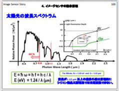
Pinned Photodiode 型の 太陽電池の提案に生かして、高性能で安価
な、量子効率が高いシリコン太陽電池が製造できないかと思っています。
AIPS Library Under Construction Now
*********************************************************************
Please write me freely anything related to my activities:
*********************************************************************
hagiwara-yoshiaki@aiplab.com for my activity at http://www.aiplab.com/
hagiwara@ssis.or.jp for my activity at http://www.ssis.or.jp/en/index.html
*********************************************************************
******************************
Return to Top Page
http://www.aiplab.com/
*********************************
**************************************************************
This is index_2020_12_07_010.html
**************************************************************
Jump to Part 001 002 003 004 005 006 007 008 009 010 011 012 013
**************************************************************