**************************************************************
This is index_2020_12_07_003.html

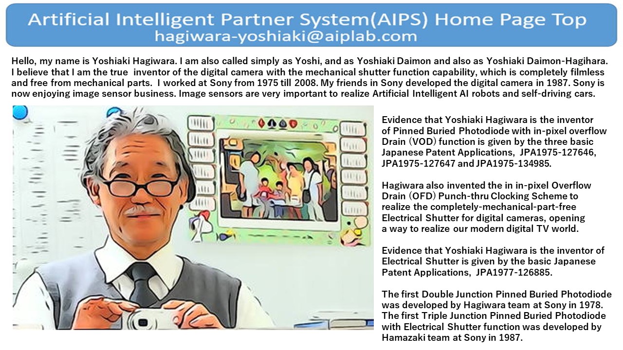
Hagiwara at Sony invented Pinned Photodiode in 1975.
http://www.aiplab.com/Hagiwara_invented_PPD_and_Sony_HAD_in_1975.pdf
+++++++++++++++++++++++++++++++++++++++++++++++++++++++++++
The PNP Double Junction Pinned Photodiode (HAD) type Solar Cell
+++++++++++++++++++++++++++++++++++++++++++++++++++++++++++
- keywords
Pinned Photodiode
Hole Accumulation Diode (HAD)
Empty Potential Well
Barrier Potential
Solar Cell
- Short Topic Description
++++++++++++++++++++++++++++++++++++++++++++++++++++++++++++
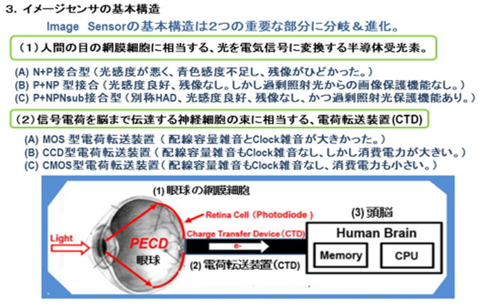
Solid State Image Sensor has two parts ( A and B ).
++++++++++++++++++++++++++++++++++++++++++++++++++++++++++++
The part A is the photo detector which converts
the photo energy ( light ) to the electrical energy ( charge ).
The part B is the charge transfer device (CTD) which trasports
the electrical signal charge to the signal processing unit ( brain ).
++++++++++++++++++++++++++++++++++++++++++++++++++++++++++++
The part A, the photo detector, evolved from A1, A2, A3 and A4 types.
++++++++++++++++++++++++++++++++++++++++++++++++++++++++++++
They are
A1 = the N+P Single Junction Type Dynamic Photo Diode
A2 = the CCD/MOS Type Dynamic Photo Capacitor
A3 = the P+NP Double Junction Type Dynamic Photo Transistor
and A4 = the P+NPN Triple Junction Type Dynamic Photo Thyristor.
+++++++++++++++++++++++++++++++++++++++++++++++++++++++++++++++++++++
The part B, the charge transfer device (CTD) evolved from B1, B2 and B3
types.
+++++++++++++++++++++++++++++++++++++++++++++++++++++++++++++++++++++
They are
B1 = the MOS type charge transfer device (CTD).
B2 = the CCD type charge transfer device (CTD).
and B3 = the CMOS Active Pixel charge transfer device (CTD).
++++++++++++++++++++++++++++++++++++++++++++++++++++++++++++
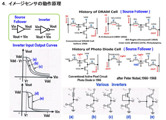
Invention of CCD in 1969 by Boyle and Smith
++++++++++++++++++++++++++++++++++++++++++++++++++++++++++++
The B2 type CCD/MOS type CTD and the A2 type CCD/MOS Dynamic
Photo Capacitor type Photo Detector was invented by Boyle and Smith in 1969.
The B2 type CCD/MOS type CTD has the complete signal charge transfer
with no image lag feature. But they have the very large surface dark current
because the MOS capacitor has the large surface electric field which generates
the large surface dark current. Besides, the MOS ( metal, oxide and semiconductor)
photo capacitor has the metal electrode which cannot pass the short wave
blue
light. Hence inherently CCD image sensor has a poor color reproduction capability
and the large surface dark current even though CCD has the low image lag
feature.
+++++++++++++++++++++++++++++++++++++++++++++++++++++++++++++++++++
Invention of Active in-Pixel Amplifier Circuit in 1969 by Peter Noble
+++++++++++++++++++++++++++++++++++++++++++++++++++++++++++++++++++
The Active in-Pixel source follower type current amplifier circuit
of the B3 type CTD was invented by Peter Noble way back in 1996
but never became possbile until recently when the sub micron
CMOS process scaling tehnology finally becomes well advanced.
+++++++++++++++++++++++++++++++++++++++++++++++++++++++++++++++++++
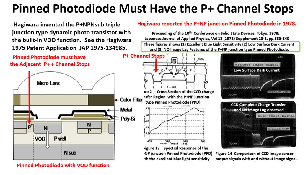
The P+NP Double Junction type Dynamic Photo Transistor was
invented by Yoshiaki Hagiwara at Sony in 1975. See the Japanese
Patent Applications, JPA 1975-127646, 1975-127647 and 1975-134985.
+++++++++++++++++++++++++++++++++++++++++++++++++++++++++++++++++++
The P+NP Double Junction type Dynamic Photo Transistor has
the complete charge transfer function with no image lag feature,
which is nothing new about it since the CCD/MOS photo capacitor
also has the same feature.
However, the P+NP Double Junction type Dynamic Photo Transistor
has the unique features of the excellent short wave blue light
sensitivity and the very low surface dark current feature since
this P+NP Double Junction type Dynamic Photo Transistor has
the Pinned surface P+P Hole Accumulation Barrier Field helping
the photo electron and hole pair separations at the silicon surface
where the short wave blue light cannot penetrate into the silicon
crystal more than 0.2 micro meter in depth into the silicon.
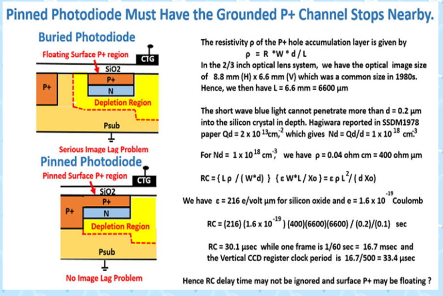
Hagiwara at Sony developped in 1978 this P+NP Double Junction type
Photodiode, which was also a buried photodiode with the charge collecting
buried N region with the P+ hole accumulation surface potential, pinned and
fixed by the adjacen P+ channel stops with the excellent blue light sensitivity.
The first P+NP junction type Photodiode was used in the Frame Transfer
CCD image sensor as reported in SSDM1978 by Yoshiaki Hagiwara at Sony.
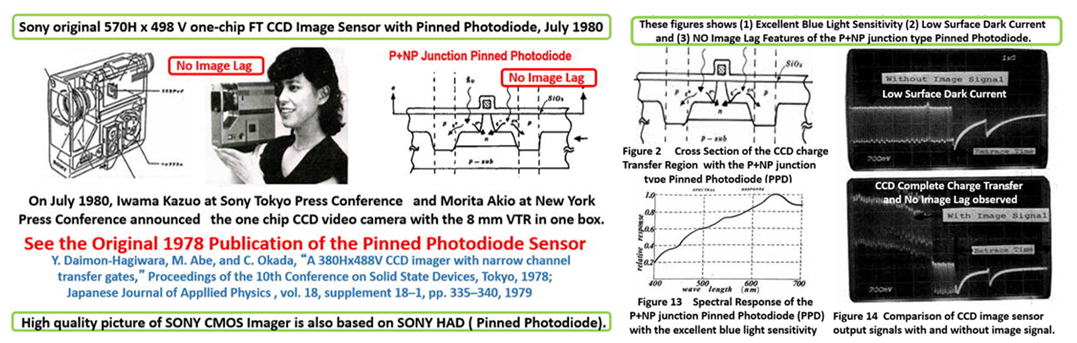
The P+NP Double Junction type Photodiode reported in SSDM1978 was also
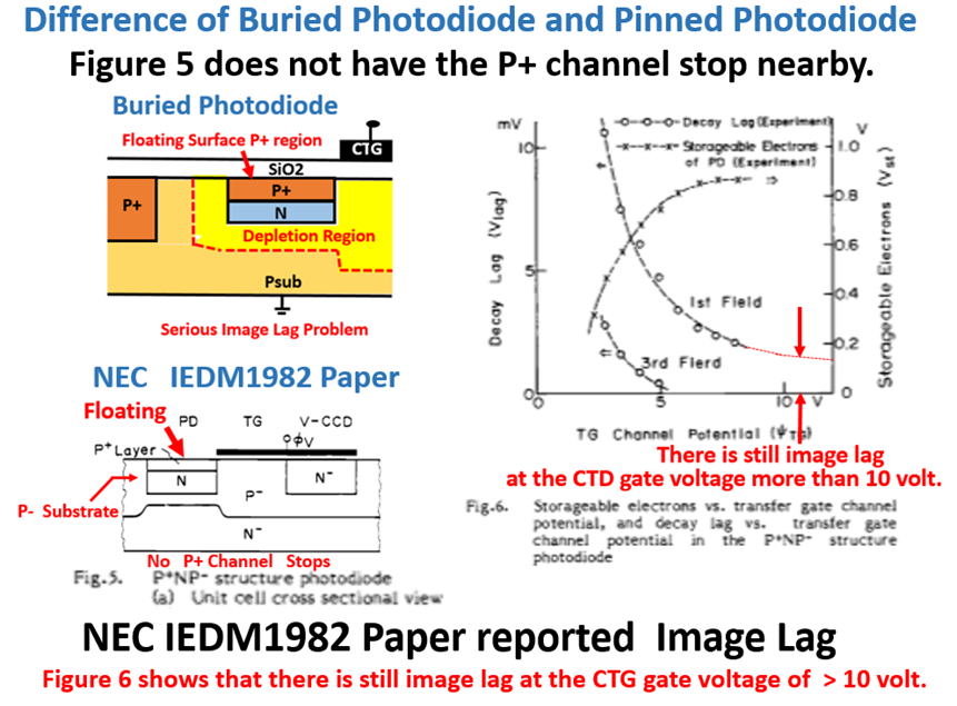
later used in the Interline CCD image sensor in 1982 by NEC, and was called
as Buried Photodiode in IEDM1982 by NEC. NEC explained the details of the
Buried Photodiode with the complete charge transfer feature with no image
lag. However, the image sensor reported by NEC in IEDM1982 shows the
measured data of some image lag ??? I do not understand why NEC 1982
image sensor had the image lag as seen in Fig. 6. The reason may be
due to the fact the surface P+ region of the NEC P+NP junction photodiode
is NOT pinned and NOT grounded ??? The surface P+ region may be floating
?
In IEDM1984, KODAK also used the P+NP Double Junction type Photodiode
in the Interline CCD image sensor and called it as Pinned Photodiode. KODAK
clearly stated that the surface P+ hole accumulation reigon is pinned and
grounded with the surface flat potential with no electric field to generate
the surfave dark current.
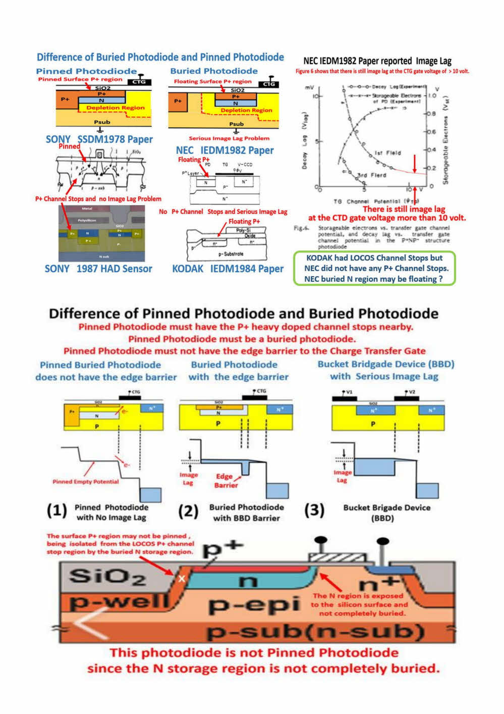
However, the Buired Photodiode reported by NEC in IEDM1982 and the Pinned
Photodiode reported by KODAK in IEDM1984 and the P+NPN triple junction
type photodiode reported by Sony in 1987 and called as the Hole Accumulation
Diode (HAD) are all the same P+NP(N) junction type Multi Junction Photodiodes,
invented by Hagiwara in 1975 and developed also by Hagiwara in 1978 and
used
in the Frame Transfer CCD image sensor as reported in SSDM1978 by Hagiwara.
Some of my friends said this Fossum 2014 review paper is very
doubtful and misleading. But I would like to say, this Fossum
2014 paper is a fake review paper, being not reporting the truth.
![]()
However, no one in the image sensor society could judge what
is the truth simply because they could not read and understand
the 1975 Japanese Patent files written in Japanese language.
I think I am the one actually to be blamed the most because
I was very much obedient to Sony manegement people who
were very much afraid of spreading Sony original knowhow
of image sensor technology and experience to the competing
rival companies. I recall that Sony management level people
were very negative even in filing a patent. I had a hard time
to explain the importance of the three 1975 patents to them.
But I myself completely forgotten the details of my inventions
by 1982. By that time I was very much interested in the
digital camera system and digital image processing system
LSI chips for the future AI robotics applications, which has
been my original dream since my prime school years and
even now. I now only wish my original 1975 Japanese patent
applications, JPA 1975-124646, 1975-124647 and 1975-134985
are well reviewed properly. Then I am sure that every one will
be convinced and understand that I am the true inventor of
the super light sensitive, low surface dark current noise and
image lag free, multi junction type dynamic photo transistor
and dynamic photo thyristor with the VOD and the mechanical
free electrical shutter function for fast filmless action cameras.
AIPS Library Under Construction Now
*********************************************************************
Please write me freely anything related to my activities:
*********************************************************************
hagiwara-yoshiaki@aiplab.com for my activity at http://www.aiplab.com/
hagiwara@ssis.or.jp for my activity at http://www.ssis.or.jp/en/index.html
*********************************************************************
******************************
Return to Top Page
http://www.aiplab.com/
*********************************
**************************************************************
This is index_2020_12_07_003.html
**************************************************************
Jump to Part 001 002 003 004 005 006 007 008 009 010 011 012 013
**************************************************************