
**************************************************************
This is index_2020_12_07_009.html
**************************************************************
Jump to Part 001 002 003 004 005 006 007 008 009 010 011 012 013
**************************************************************
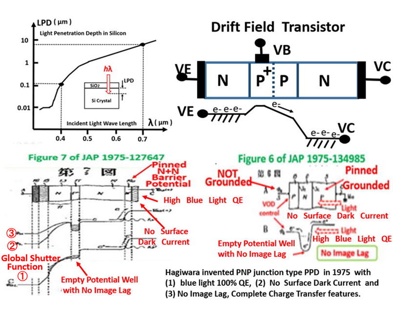
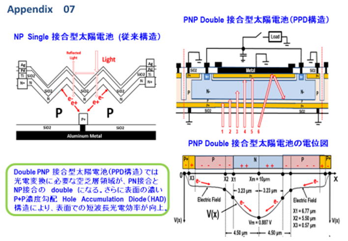
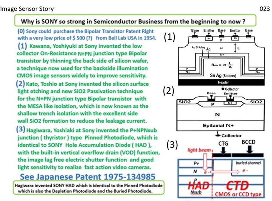
Hinted by the base P+P sloped doping profile
of the Drift Field Transistor shown above,
Hagiwara at Sony in 1975 invented N+NP+Psub
and P+PNPNsub junction thyristor type
Dynamic Photo Transistors whch were later
called as Pinned Photodiode or Sony Hole
Accumukation Diode (HAD) with the vertical
overflow drain (VOD) function which was
needed to realize the mechanical-free
electrical shutter.
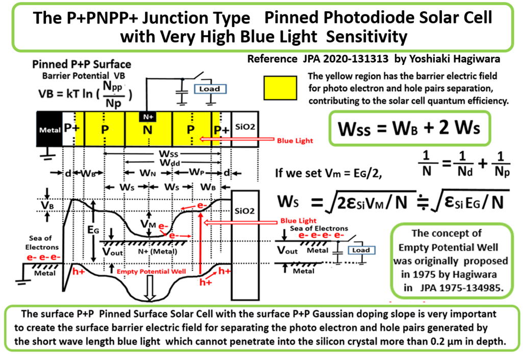
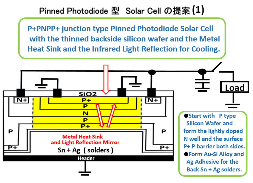
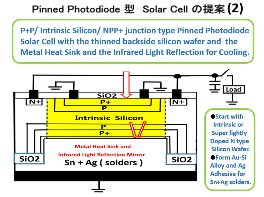
Hagiwara is now proposing a new solar cell
with the P+P Pinned Surface and with the
Completely Empty Buried N Well Potential
to realize very high efficiency solar cells.
Simple Pinned Photodiode Solar Cell Structure (1)
with the N well formation on the lightly doped P type substrate wafer.
Simple Pinned Photodiode Solar Cell Structure (1)
on the instrinsic substrate ( or super lihtly doped N type ) silicon wafer.
http://www.aiplab.com/P2020_Pinned_Photodiode_Solar_Cell_1.pdf
http://www.aiplab.com/P2020_Pinned_Photodiode_Solar_Cell_2.pdf
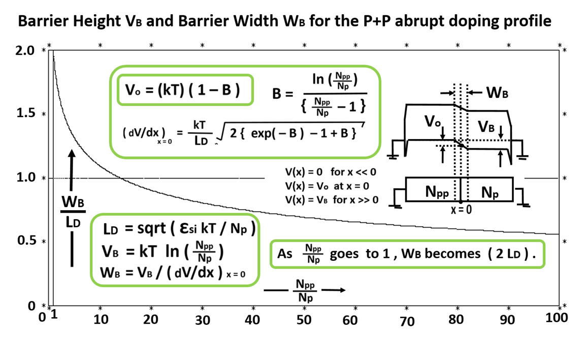
The Surface Barrier width WB would be
about the debye length ( L debye )
of the P region of the doping level of Np.
If we have Np = 100 e / um+3 ,
we have the debye length
( L debye ) = sqrt (εsi *kT/Np) = 0.4 um,
which is quilte a distance
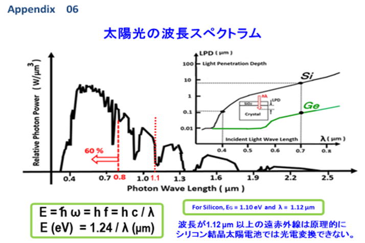
since the short wave blue light
cannot penetrate the silicon surface
more than 0.2 um in depth.
If we have Np = 10000 e / um+3 ,
we still have the debye length
( L debye ) = sqrt (εsi *kT/Np) = 0.04 um,
http://www.aiplab.com/Surface_Barrier_Width.html
.
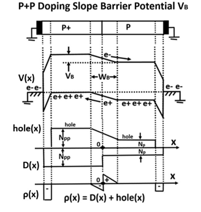
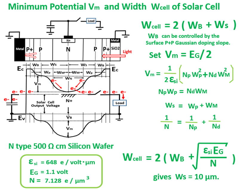
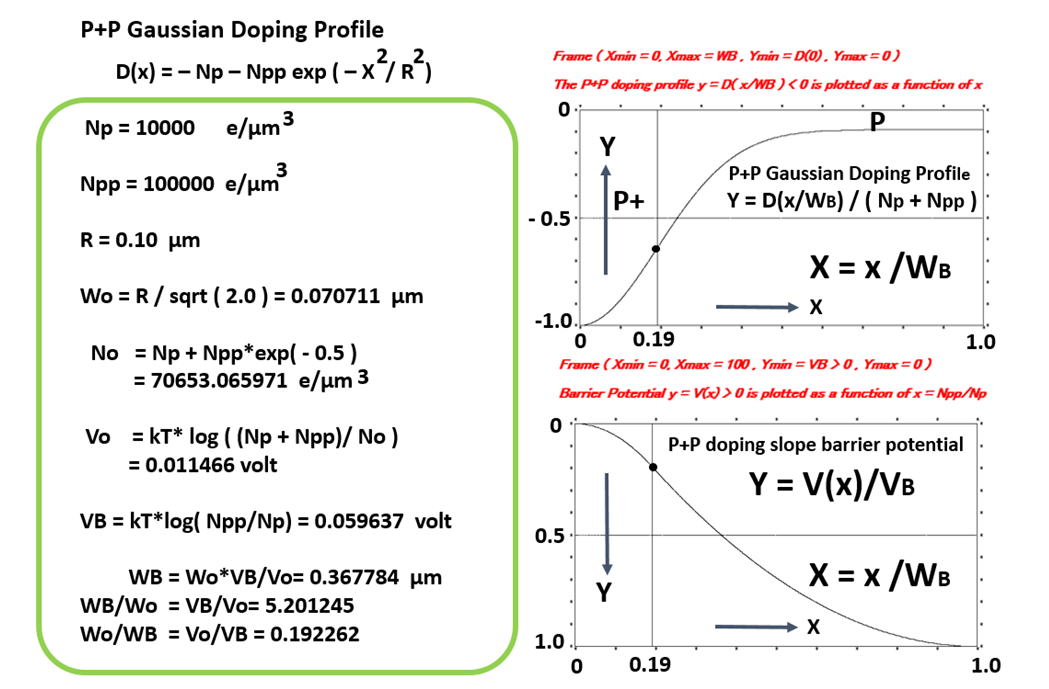
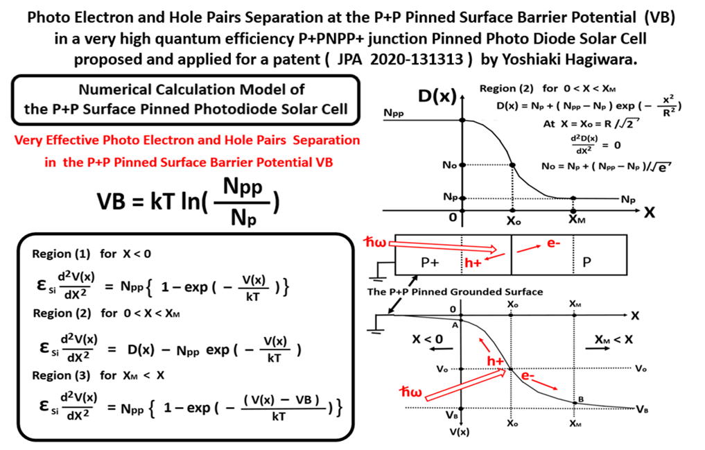
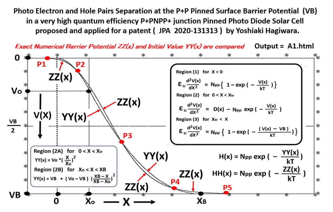
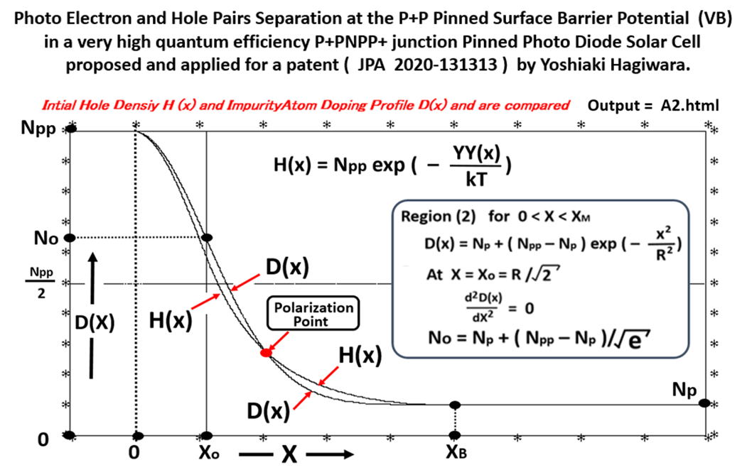
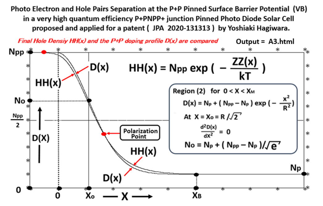
The P+PNP junction type Pinned Photodiode has
an excellent blue light sensitivey because of the
Gaussian P+P Surface Doping Profile D(x) .
A much wider Barrier Potential Width WB with
Surface Barrier Electric Field is formed for
photo electron and hole pair separations to
realize a high quantum efficiency solar cell.
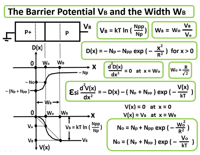
For the following calculations, for the Gaussian
P+P Surface Doping Profile D(x), the surface
impurity doping concentration D(0) is defined
as D(0) = - Np - Npp.
The sysmetric P+PNPP+ junction type
Pinned PhotodiodeSolar Cell is formed
on the super lightly doped N-type silicon
substrate with the P-well (Np) formations
and the P+ (Npp) surface ion implantations.
Hence in this case the surface impurity
doping level is denoted as - ( Np + Npp ).
http://www.aiplab.com/Surface_Barrier_Width_3.html
http://www.aiplab.com/Pinned_Photodiode_Surface_Barrier_Potential.htmll
AIPS Library Under Construction Now
*********************************************************************
Please write me freely anything related to my activities:
*********************************************************************
hagiwara-yoshiaki@aiplab.com for my activity at http://www.aiplab.com/
hagiwara@ssis.or.jp for my activity at http://www.ssis.or.jp/en/index.html
*********************************************************************
******************************
Return to Top Page
http://www.aiplab.com/
*********************************
**************************************************************
This is index_2020_12_07_009.html
**************************************************************
Jump to Part 001 002 003 004 005 006 007 008 009 010 011 012 013
**************************************************************