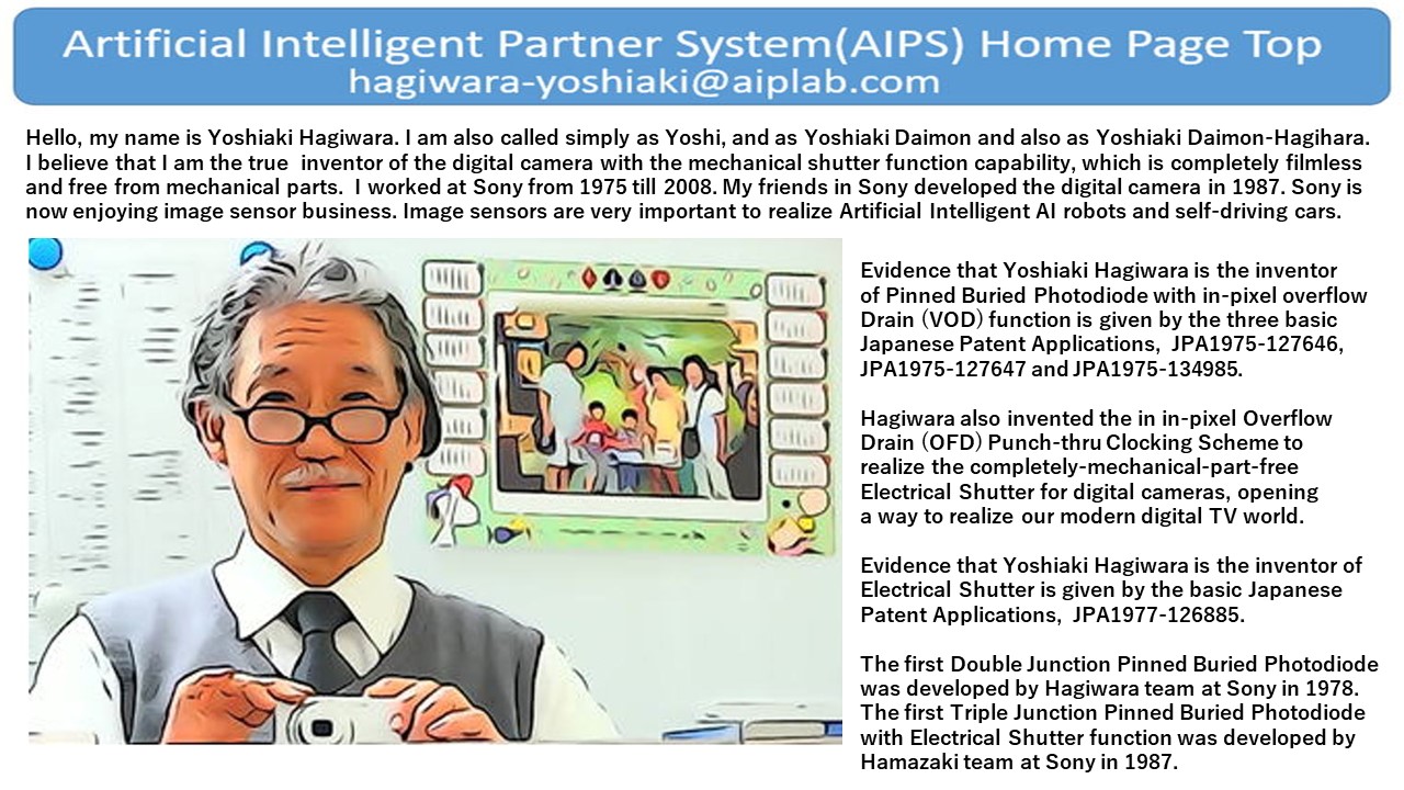
**************************************************************
This is index_2020_12_07_004.html
**************************************************************
Jump to Part 001 002 003 004 005 006 007 008 009 010 011 012 013
**************************************************************
********************************************************************
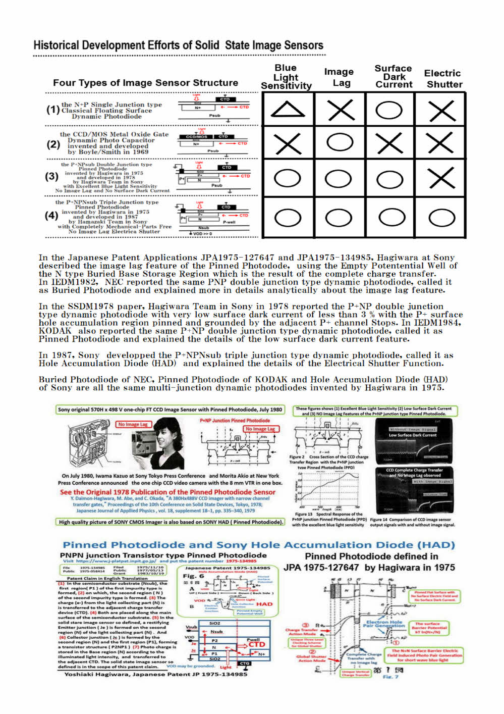
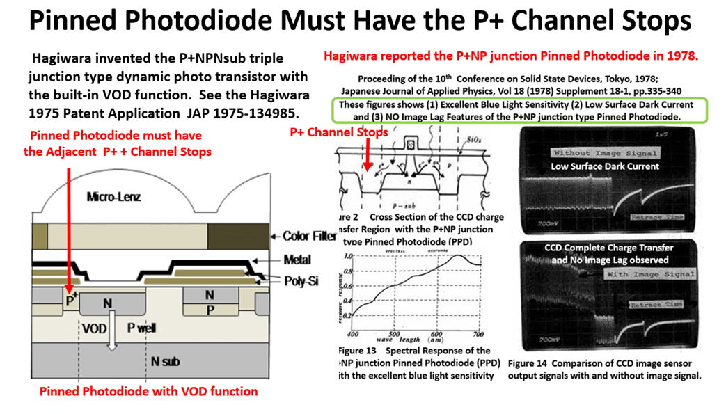
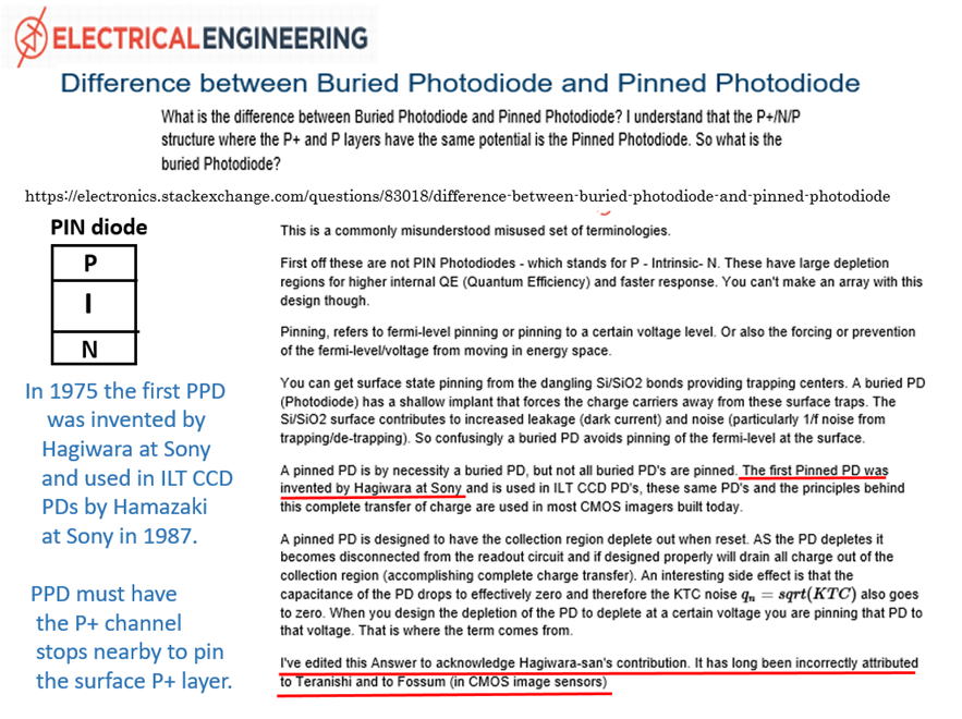
Buried Photodiode is NOT always Pinned Photodiode.
********************************************************************
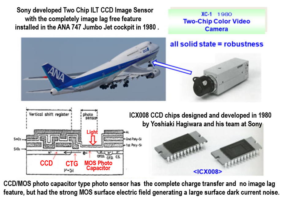
I think KODAK used PPD in the ILT CCD image sensor and reported in IEDM1984
for the first time in the world while SONY ( Hagiwara ) used PPD in the
FT CCD
image sensor and reported in SSDM1978 for the first time in the world.
********************************************************************
The surface thin and shallow P+ hole accumulation layer is formed
by the self-aligned ion implantation in the final processing stage.
The depth of the surface P+ hole accumulation layer
must be very shallow and less than 0. 2 micro meter
since the short wave blue light cannot penetrate
into the silicon cystal more than 0. 2 micro meter
in depth. The P+ thin layer stripe of the length L
has a large resitance R and a large capacitance C,
and then, also a large time delay constant of T=RC ,
which makes the P+ thin hole accumulaion layer
effectively floating. Therefore, this photodiode may
have a serious image lag ?? Any photodiode with
the serious image lag cannot be Pinned Photodiode.
This photodiode may not be Pinned Photodiode ????
+++++++++++++++++++++++++++++++++++++++++++++++++++++++++++++++++++
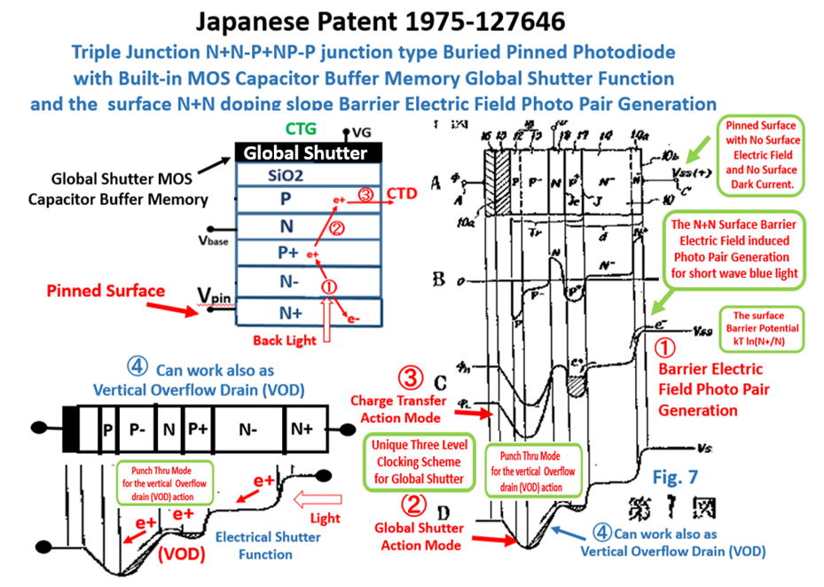
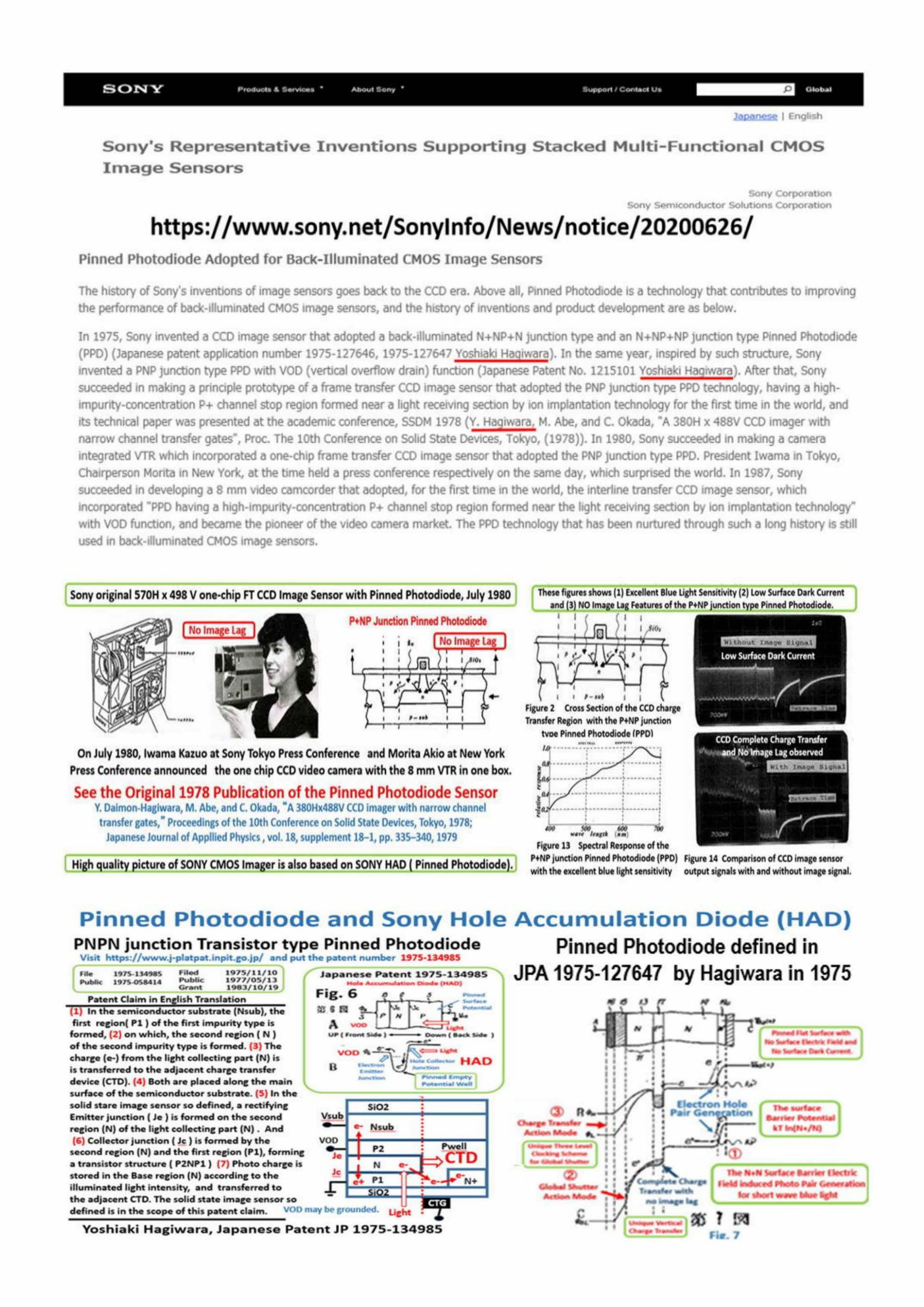
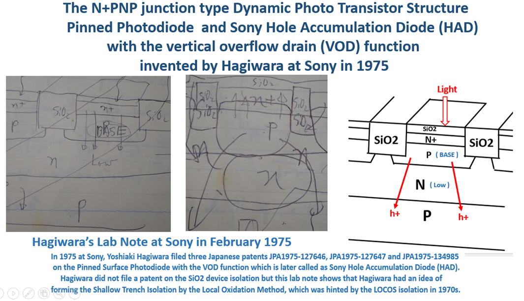
The P+NPN Triple Junction type Dynamic Thyristor Photo Sensor, which
was developped in 1987 by Hamazaki team later called as Hole Accumulation
diode(HAD) by Sony has the vertical overflow drain (VOD) and the eletrical
shutter funtion. This P+NPN Triple Junction type Dynamic Thyristor Photo
Sensor was also invented by Yoshiaki Hagiwara at Sony in 1975. See also
the Patent Applications, JPA 1975-127646, 1975-127647 and 1975-134985.
+++++++++++++++++++++++++++++++++++++++++++++++++++++++++++++++++++
Hagiwara at Sony is the inventor and also the developper of the P+NP double
junction type Pinned Photodiode. Hagiwara also invented the P+NPN triple
junction type Pinned Photodiode with the vertical overflow drain (VOD) and
the electrical shutter function.
In 1987, the Hamazaki team in Sony developed the P+NPN triple junction type
Pinned Photodiode, named it as Hole Acculation Diode (HAD) and used it in
Interline Transfer Type CCD Image Sensors.
![]()
+++++++++++++++++++++++++++++++++++++++++++++++++++++++++++++++++++
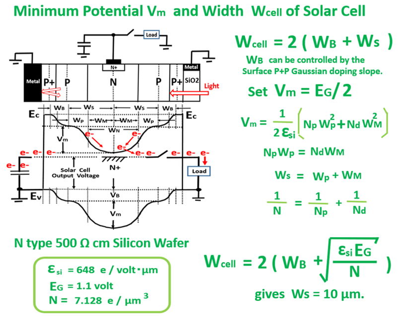
The P+PNPP+ double junction type Pinned Photodiode type Solar Cell
+++++++++++++++++++++++++++++++++++++++++++++++++++++++++++++++++++
Most of the solar cells are still of the N+P single junction type.
Here now the Pinned surface P+PNPP+ double junction type Solar Cell
is proposed, which is expected to have a very large quantum efficiency
of more than junction 60% , by using the surface hole accumulation (HAD)
region with the pinned P+P surface and the surface barrier potential
which separates the hole electron pairs generated by the short wave blue
light very effectively in the pinned silicon P+P surface barrier electric field.
A very hige efficient Pinned Photodiode (HAD) type Solar Cell is expected
to be manufactured with a very cost-effective simple fabrication process.
+++++++++++++++++++++++++++++++++++++++++++++++++++++++++++++++++++++
************************************************
What is Pinned Photodiode ?
*************************************************
Pinned Photodiode is a double junction type photodiode
with the buried charge collection storage (base) region
and with the pinned surface flat potential fixed by the
adjacent channel stops. This unique photodiode has
many wonderful features that realized the modern solid
state electric eye for AI Robot Vision.
The pinned surface potential gives the flat surface
potential with no surface electric field. Hence there
is no surface electric induced surface dark current.
The signal charge stored in the buried storage (base)
region can be transfered compleletly to the adjacent
charge transfer gate (CTD) with no image lag feature.
The complete photo signal charge transfer results in
the completely empty potential well in the buried
storage (base) region which is the evidence of the
image lag free picture quality for action movie cameras.
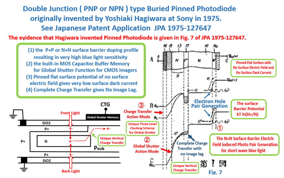
Yoshiaki Hagiwara at Sony in 197,for the first time in
the world, drew this empty potential wells in the Fig. 6
of his Japanese patent application JPA 1975-134985 and
also Fig. 7 of JPA 1975-127646 and JPA 1975-127647.
************************************************
*******************************************************************
Fig.7 of JPA 1975-127647, the original Japanese patent on the double
junction type Pinned Photodiode shows the empty potential well which
implies the complete charge transfer operation of no image lag feature.
This is the evidence that Hagiwara is the true inventor of Pinned Photodiode.
******************************************************************

Sony developed the double junction type Pinned Photodiode in 1978 and
reported
in SSDM1978 paper. And Then Sony used this double junction type Pinned
Photodiode for the one chip video movie camera in 1980.
Sony developed the triple junction type Pinned Photodiode in 1987 with
the
complete Electric Shutter Function with no image lag and for action pictures.
This triple junction type Pinned Photodiode shown above and defined in
the
Japanese Patent Application JPA 1975-134985 was originally hinted by the
triple junction type Pinned Photodiode defined in Japanese Patent Application
JPA 1975-127646 shown below which is also inventedby Hagiwara in 1975.
Hagiwara is the inventor of the Electrical Shutter Function of Pinned Photodiode.
Electric Shutter Function is possible only in the image lag free photo
sensors.
Only the CCD/MOS capacior type photo sensors
and Pinned Photodiode type photo sensors are
the complete image lag free photo sensors.
Only the classical CCD/MOS capacitor type
and the triple junction type Pinned Photodiode,
invented by Hagiwara in 1975, can serve for
the completely filmless cameras, which is also
completely free from any mechanical parts.
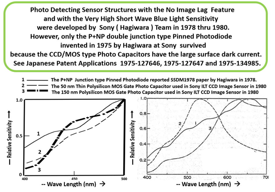
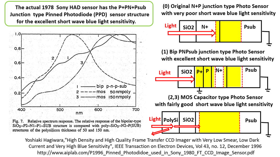
CCD/MOS photo capacitor has the serioous large surface dark current problem.
Hagiwara invented the double and triple junction Pinned Photodiodes with
the
Pinned Surface P+ Emitter region and the Buried Base Photo Charge Storage
region with the complete charge transfer function capability with no image
lag.
http://www.aiplab.com/NPNP_junction_Pinned_Photodiode_in_1975_by_Hagiwara_A.jpg
http://www.aiplab.com/JP1975-127647_A.jpg
http://www.aiplab.com/JP1975-134985_Patent_Claim_in_English.jpg
http://www.aiplab.com/JP1975-127646_A.jpg
http://www.aiplab.com/P1978_SSDM1978_Paper_on_Pinned_Photodiode_A.jpg
http://www.aiplab.com/Pinned_Photodiode_Reported_in_Hagiwara_SSDM1978_Paper.jpg
http://www.aiplab.com/What_is_True_Pinned_Photodiode.jpg
AIPS Library Under Construction Now
*********************************************************************
Please write me freely anything related to my activities:
*********************************************************************
hagiwara-yoshiaki@aiplab.com for my activity at http://www.aiplab.com/
hagiwara@ssis.or.jp for my activity at http://www.ssis.or.jp/en/index.html
*********************************************************************
******************************
Return to Top Page
http://www.aiplab.com/
*********************************
**************************************************************
This is index_2020_12_07_004.html
**************************************************************
Jump to Part 001 002 003 004 005 006 007 008 009 010 011 012 013
**************************************************************