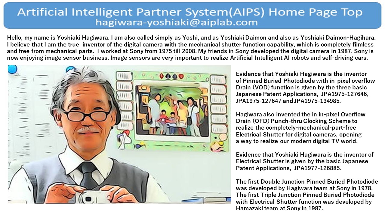
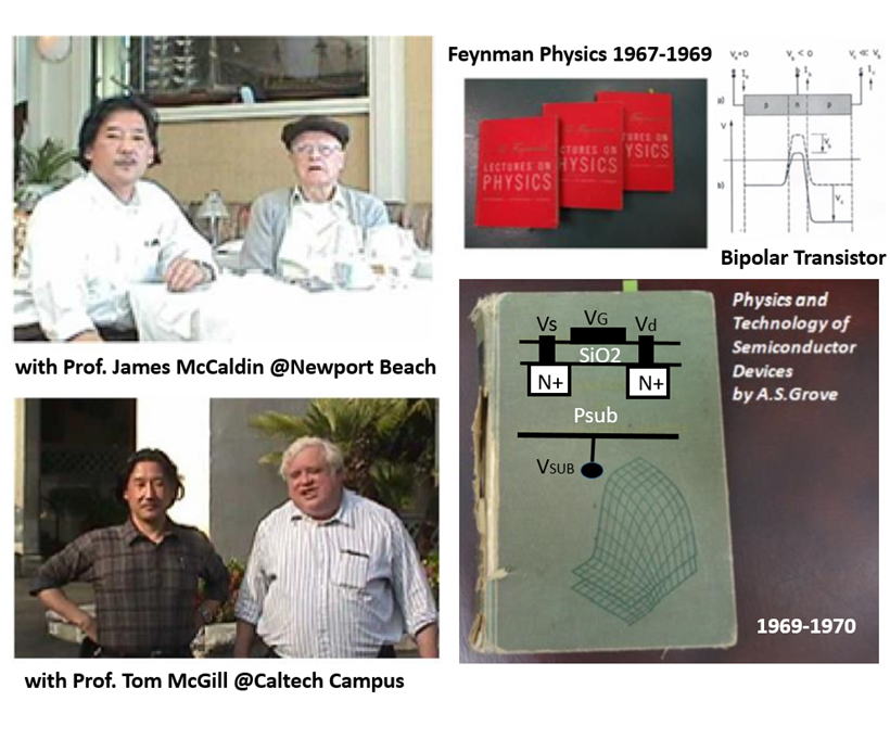
*********************************************************
My Wonderful Memory Picture
*********************************************************
*********************************************************
< List of Books >
*********************************************************
*********************************************************
(1) Coauthor "CCD Image Sensor and Applications",
Triceps Press, November 1980
http://www.triceps.co.jp/
(2) Coauthor "Computer Engineering Handbook",
CRC Press, December 2003
https://en.wikipedia.org/wiki/CRC_Press
(3) Single Author "The world of AI Digital Circuits",
Seizansha Press, March 2016
https://www.seizansha.co.jp/
https://www.seizansha.co.jp/ISBN/ISBN978-4-88359-339-2.html
***********************************
List of Journal Publication
***********************************
(1) Coauthor Paper1973
"The Influence of Interface States on Incomplete Charge Transfer
in Overlapping Gate Charge Coupled Devices",
IEEE Journal of Solid State Circuits, Vol. SC 8, No.2, April 1973
(2) Head Author Paper1974
"Final Stage of the Charge Transfer Process in Charge Coupled Devices"
IEEE Transactions on Electron Devices, Vol. ED-21, No.4, April 1974
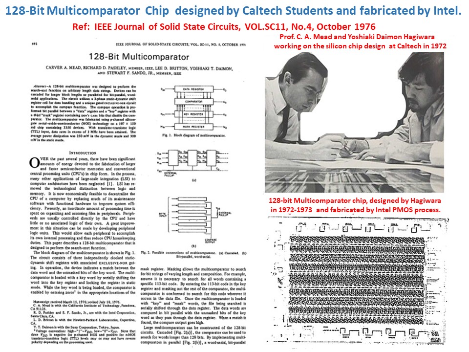
(3) Coauthor Paper1976
"128-Bit Multi Comparator", IEEE Journal of Solid State Circuits,
VOL.SC11, No.4, October 1976
http://www.aiplab.com/P1976_128_bit_Comparator.pdf
(4) Single Author Paper1977
"Two Phase CCD with Narrow Channel Transfer Regions"
SSDM1978 Conference Paper September 1978 and
Japanese Journal of Applied Physics,
Vol 17 (1978) Supplement 17-1, pp.255-261
(5) Coauthor Paper1978
"An Interline Transfer CCD Imager with High Density Structure",
Journal of Electronics Information and Communication Technologies,
SSD78-5, ICD89-20 S0532B Vol 89 No. 66 (SDM89 9-18), 31-40,
April 1978.
(6) Head Author Paper1978
"A 380H X 488V CCD Imager with Narrow Channel Transfer Gates"
SSDM1978 Conference Paper September 1978 and Japanese Journal
of Applied Physics, Volume 18 Sup 18-1, pp.335-340 November 1979
http://www.aiplab.com/P1978_Pinned_Photodiode_1978_Paper_by_Hagiwara.pdf
(7) Coauthor Paper1980
"Interline Transfer CCD Image Sensor", Technical Journal of
Japan Television Society, ED481 S0209A (0386-4227)
Vol3 No.33 , pp.47-52, January 24, 1980
(8) Coauthor paper1981
"2/3 inch Optical Lenz Single Chip Color Camera Using Narrow Channel
CCD Imager with Overflow Drain", technical Report at The technical meeting
of circuit and system technology workshop sponsored by Japan Television
Society February 1981, TEBS 76-6, ED611, pp. 31- 36.
(9) Coauthor Paper1981
"Single Chip Color Camera Using Narrow Channel CCD Imager with
Overflow Drain", Technical Report at Japan Society of Television
Workshop on Dec 16, 1981, TEBS 76-6, ED611
(10) Coauthor Paper1989
"A 25-ns 4-Mbit CMOS SRAM with Dynamic Bit-Line Loads"
IEEE Journal of Solid State Circuits, vol.24, no.5, October 1989.
http://www.aiplab.com/P1989_SONY_4MSRAM_1989.pdf
(11) Single Author Paper1989
"DRAM/SRAM Technology and Problem"
Proceedings of the Institute of Electrostatics Japan.
127 Vol. 22 No. 6, 1998, pp.177-28
(12) Single Author Paper1996
"High Density and High Quality Frame Transfer CCD Imager with
Very Low Smear, Low Dark Current and Very High Blue Sensitivity",
IEEE Transaction on Electron Devices, Vol 43, no. 12, December 1996
http://www.aiplab.com/P1996_Pinned_Photodidoe_used_in_Sony_1980_FT_CCD_Image_Sensor.pdf
(13) Single Author Paper 2013
"The p-n-p-n Diode in Future Linear Motor Cars and in Modern Images」
IEEE Solid-State Circuit Magazine, Summer Issue pp. 6-8, June 2013
http://www.aiplab.com/P2013_ISSCC2013PanelTalk.pdf
(14) Coauthor Paper2014
"Design of Time to Frequency Domain Discrete Fourier Transfer Hardware Engine
and its performance estimation" Digest of Technical Papers at the Japan
Electron Society sponsored Integrated Circuit Workshop in Izumo, Japan, July 2014
**********************
Conference Publications
**********************
(1) Head Author Paper1974
"Charge Transfer of Buried Channel Charge Coupled Devices"
Proceeding of International Solid State Circuit Conference (ISSCC),
San Francisco, February 1974.
(2) Single Author Paper1977
"Two Phase CCD with Narrow Channel Transfer Regions"
SSDM1978 Conference Paper September 1978 ,
Proceeding of the 9th Conference on Solid State Devices, Tokyo 1977;
Japanese Journal of Applied Physics,
Vol 17 (1978) Supplement 17-1, pp.255-261
(3) Coauthor Paper1978
"An Interline Transfer CCD Image Sensor with High Density Structure",
Technical Report presented at Japan SSD Conference, Tokyo May 1978, SSD 78-5.
(4) Head Author Paper1978
"A 380H X 488V CCD Imager with Narrow Channel Transfer Gates"
SSDM1978 Conference Paper September 1978 and Japanese Journal
of Applied Physics, Volume 18 Sup 18-1, pp.335-340 November 1979
http://www.aiplab.com/P1978_Pinned_Photodiode_1978_Paper_by_Hagiwara.pdf
(5) Single Author, Invited Paper1979
"ADVANCES in CCD Imager " Technical Digest of IEEE
International Conference of CCD Image Sensors (IEEE CCD'79),
Edinburgh, Scotland UK, September 1979
https://www.imagesensors.org/Past%20Workshops/1979%20CCD79/03-1%20Hagiwara.pdf
(6)Single Author, Invited Paper1980
"A CCD color imager with narrow-channel transfer gates", Proceeding of
the 157th Electrochemical Society Meeting, May 11-16, 1980, St. Luis, USA
(7) Coauthor Paper1989
"A 25-ns 4-Mbit CMOS SRAM with Dynamic Bit-Line Loads"
Proceeding of the 1989 International Conference of the Solid
State Circuits (IEEE ISSCC1989), February 1989.
http://www.aiplab.com/P1989_SONY_4MSRAM_1989.pdf
(8)Single Author, Invited Talk1997
"Sony Semiconductor History", addressed at the 23th Research Seminar
in Tokyo Communication University, Nov 28, 1997
(9)Single Author, Invited Talk2001
"Micro-Electronics for Home Entertainment" Technical Digest of IEEE
ESSCIRC International Conference (ESSCIRC2001), Villach, Austria,
September, 2001
http://www.aiplab.com/P2001_ESSCIRC2001.pdf
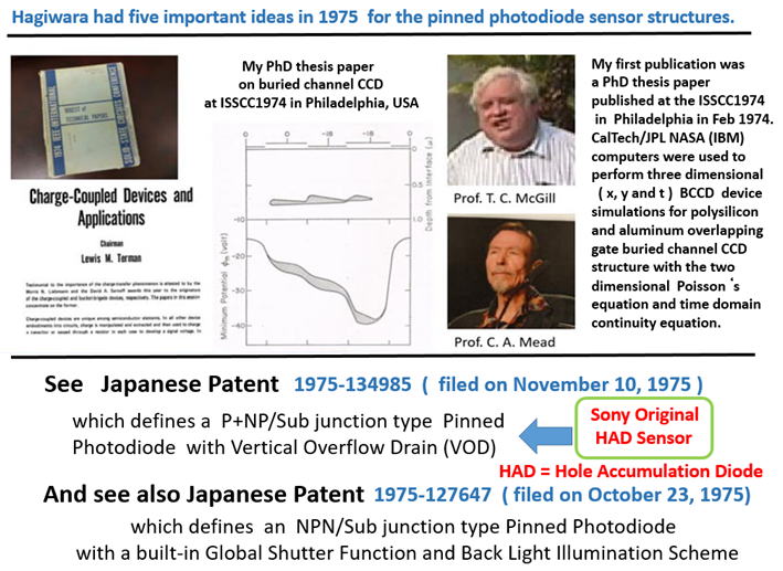
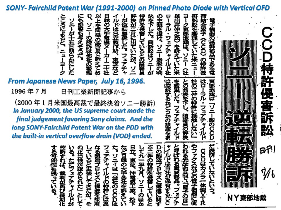
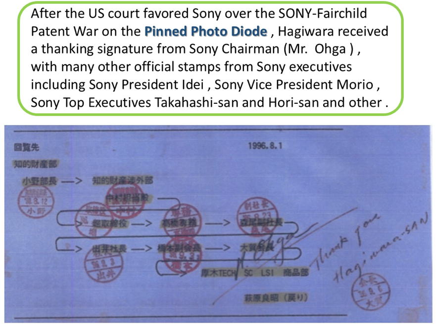
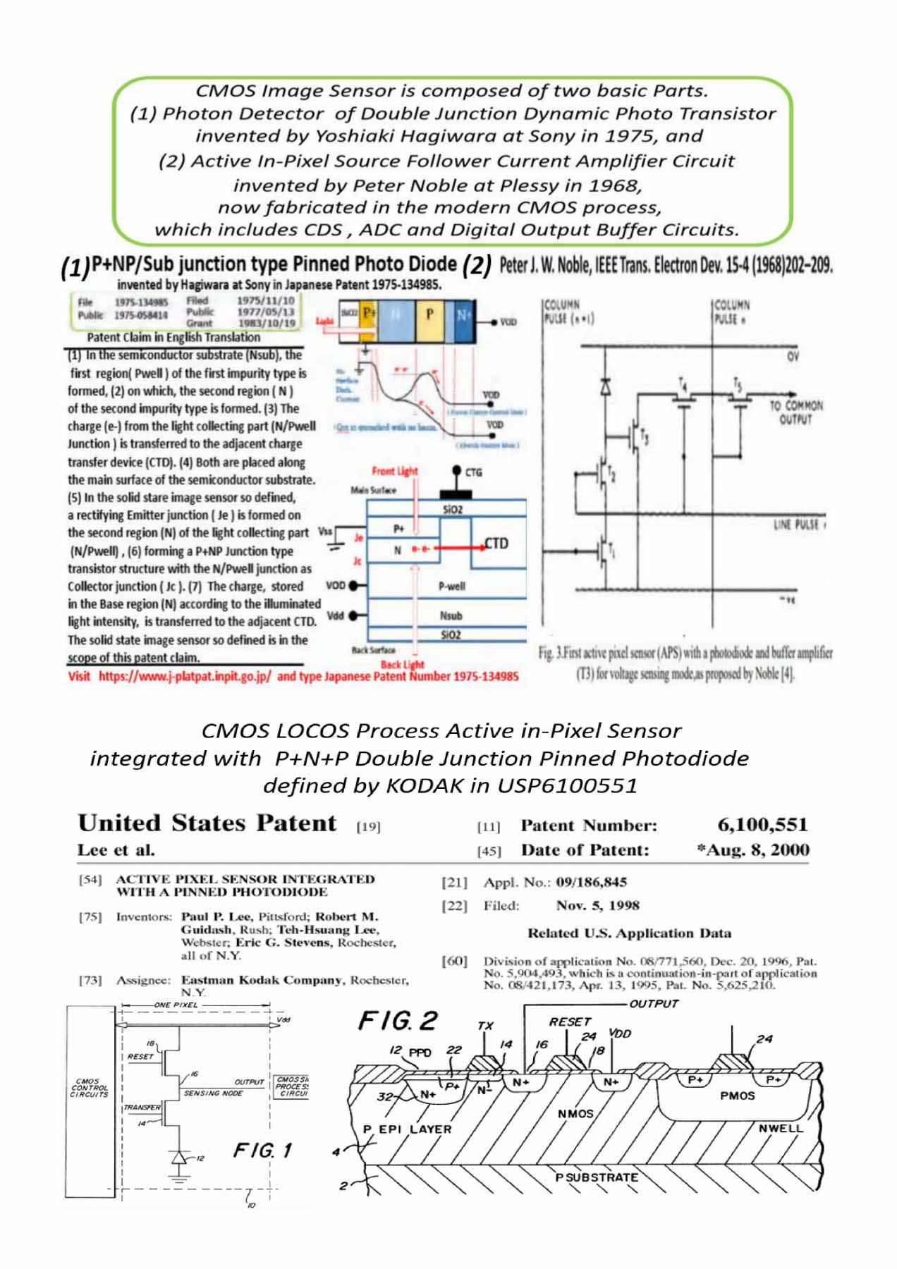
SONY KODAK Patent Agreements on ImageSenosor were finalized on January 2007.
Since the invention of the P+NPNsub junction type Pinned Photodiode by
Hagiwara in 1975,
Hagiwara had to defend his 1975 Pinned Photodiode inventions,
Japanese patents JPA 1975-127646, 1975-127647, and 1975-134985
from Fairchild , NEC, and KODAK throughout his life-long career in Sony.
Next year, Hagiwara retired from Sony finally in July 2008, at age 60.

(10)Single Author, Invited Talk2008
"SOI Design in Cell Processor and Beyond", Technical Digest of
IEEE ESSCIRC International Conference (ESSCIRC2008),
Edinburgh, Scotland UK, September 2008
http://www.aiplab.com/P2008_ESSCIRC2008Hagiwara.pdf
(11) Single Author, Invited Plenary Panel Talk
"The p-n-p-n Diode in Future Linear Motor Cars and in Modern Images」
IEEE Solid State Society ISSCC2013 Conference, February 2013.
http://www.aiplab.com/P2013_ISSCC2013PanelTalk.pdf
(12) Coauthor Paper2014
"Design of Time to Frequency Domain Discrete Fourier Transfer Hardware Engine
and its performance estimation" Digest of Technical Papers at the Japan
Electron Society sponsored Integrated Circuit Workshop in Izumo, Japan, July 2014
My 2014 invention of a unique sampling scheme.
(13) Coauthor Paper2015
"Digital Frequency Transformation Circuit for Time-wise Unequally Sampled Data "
The journal of the IEICE 2015 Technical conference sponsored by the Institute of
Electronics, Information and Communication engineers, July 2015.
(14) Single Author2019
"Multichip CMOS Image Sensor Structure for Flash Image Acquisition"
IEEE International 3D Systems Integration Conference 2019 (3DIC2019)
Digest of Technical Papers, Sendai, Japan, Paper4017, October 2019
http://www.aiplab.com/P2019_3DIC2019Paper_on_3D_Pinned_Photodiode.pdf
(15) Single Author Paper2020
"Simulation and Device Characterization of the P+PN+P Junction Type
Pinned Photodiode and Schottky Barrier Photodiode"
IEEE Electron Device and Manufacturing Technology Conference (EDTM2020),
Digest of Technical Papers, Penang Malaysia, Paper ID 3D6, March 2020
http://www.aiplab.com/P2020_EDTM2020_PaperID_3C4_by_Hagiwara.pdf
************************
International Contribution
************************
(1) International Standardization Committee (1989-1992)
IEC TC47 Technical Committee Chair (1992)
(2) JEDEC Memory Chips Standardization Committee (2000-2004)
*************************************
Contributions to International Conferences
*************************************
(1) IEEE EDS ICMTS International Program and
Executive Committee (1991-2008)
General Chair (2003-2004)
(2) IEEE SSS ISSCC Asian Program Committee (2001-2007)
ISSCC Asian Chair (2006-2007)
(3) IEEE SSS ISSCC International Program
and Executive Committee (2007-2008)
International Program Chair (2007-2008)
(4) IEEE Computer Society Cool Chips
Organization Committer (2001-2010)
(5) IEEE Computer Society Cool Chips
Advisory Committer (2011-2020)
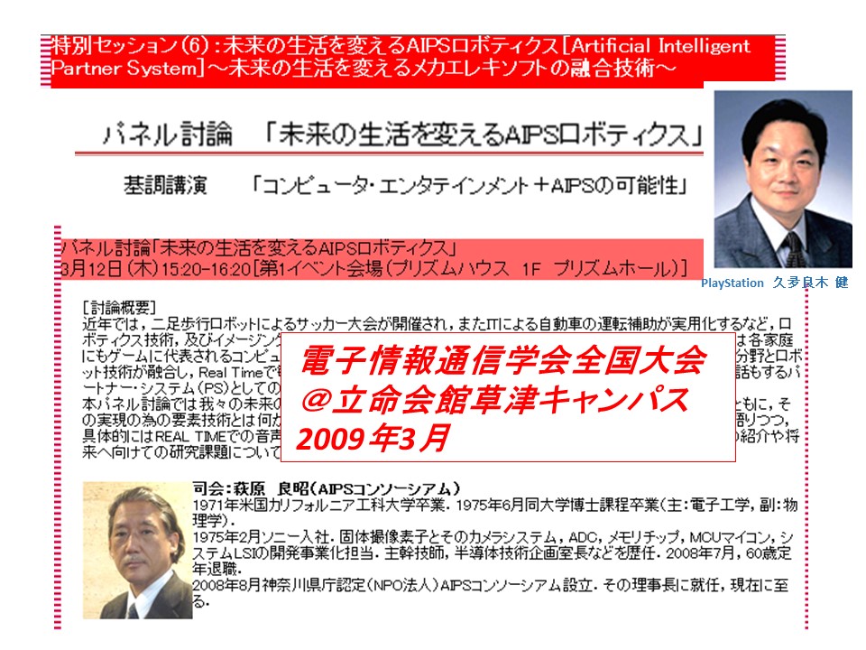
(6) Artificial Intelligent Partner System (AIPS) Consortium (NPO)
President and CEO (2008-2017)
*******
Awards
*******
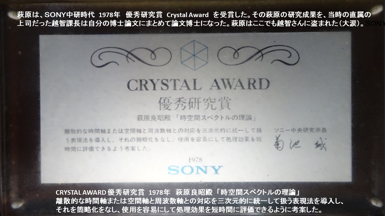
(1) Sony Central Research Center Crystal Award, March 1979.
Single Person Award for the image recognition and signal processing technology
(2) Sony Patent Award (Patent No.1308874) Third Class, May 1986.
Single Person for a new image sensor structure
(3) Sony Patent Award (Patent No. 1720715) Third Class, May 1989.
Single Person Award for a new image sensor structure
(4) Sony CEO Award, May 1989
Team Award for the 25 nanosec 4M bit Cache SRAM for digital camera system
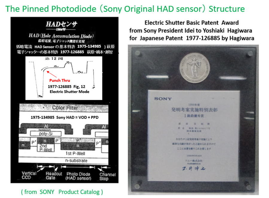
(5) Sony Patent Award (JPA 1975-134985, Patent No. 1215101) First Class, May 1996.
http://www.aiplab.com/JP1975-134985.pdf
Single Person Award for the invention of the Sony Hole Accumulation Diode
(HAD)
which is the Pinned Photodiode with the in pixel Overflow Drain (VOD) function.
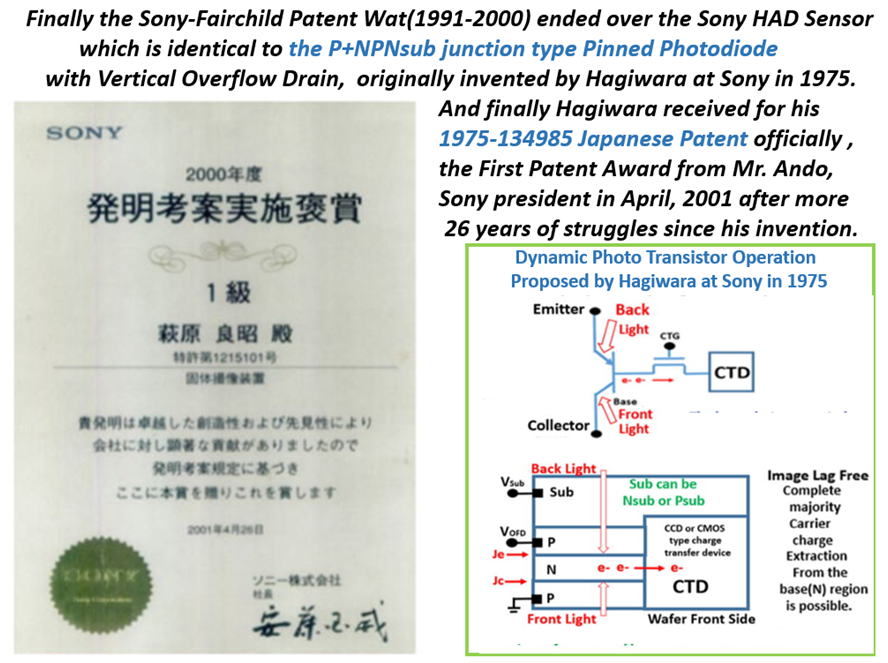
(6) Sony Semiconductor Company President Award, April 2000
Single Person Award for the imagers and digital LSI chips developments for digital camera.
(7) Sony Best Patent Award of the Year Award, May 2000.
( Patent No. 1654617, JPA1975-126885 filed on Sept 29, 1977)
http://www.aiplab.com/JP1977-126885.pdf
Team Award for the invention of all solid state in pixel electric shutter function
for fast action video pictureaquisition and flickerless picture quality, supperssing
the picture noise induced by the 60Hz or 50 Hz house power lines.
(8) IEEE Fellow Recognition Award, Jan 2001
(9) California Institute of Technology
Distinguished Alumni Award, May 2001.
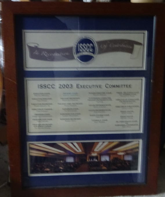
(10) ISSCC2003 Executive Committee Contribution Award
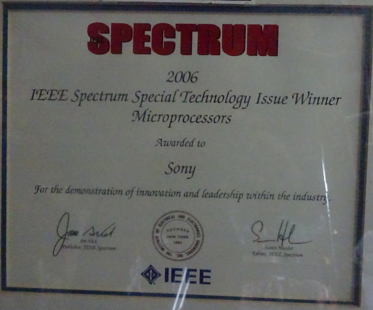
(11) IEEE2006 SPECTRUM Sony Team Award on the PS3 Cell Processor
(12) IEEE EDS ICMTS Conference Service Recognition Award
as the 2004 General Chair and a member of the steering and
technical program committees, 1991-2008.
(13) IEEE SSS ISSCC2013 Conference Recognition Award
as a presenter in the Plenary Panel on
“Antiques of the Innovative Attic” ,
February 2013.
(14) IEEE Life Fellow Recognition Award, Jan 2018
*************************************
******************************
My Work Summary
******************************
I was teaching graduate and undergraduate students at Sojo university
as a full professor of the information science department since 2009
till 2017. During the period I taught the various courses such as
Engineering Mathematics, Numerical Computational Method,
Semiconductor Device Physics, Digital Circuit and System Design
and Artificial Intelligent Robotics.
I wrote a book entitled as “The world of Digital Circuits” for
the Intelligent Partner System (AIPS) applications in 2016 which
summarizes the most of the scopes of my class teaching materials
focused to the physics of semiconductor and LSI chip designs.
My most important contribution to the world is that my inventions
and my development efforts helped and accelerated the world to
change from the analog to the digital world by replacing the film
and the mechanical shutter technologies by the all solid semiconductor
silicon chips in the field of the intelligent image sensor technology.
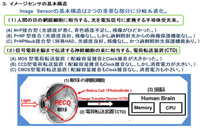
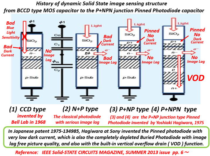
Specifically, my 1975 invention of three layer device of pnp dynamic
photo transistor structure, when the two layer photodiode of pn structure
was common at that time, was very unique and is a new dimensional
device for future 3DIC multi-chip integration for artificial intelligent
partner systems with a great deal of freedom for improving image
sensor performances, including super light sensitivity, the most
important characteristics of the image sensor device now used all
over the world.
This is the base of today’s photodiode called PPD or Pinned Photodiode,
which is widely used for various applications including smartphones,
robotics, and self-driving cars to name a few. Sony commercialized
image sensor devices based on his invention, with the trade name
of HAD (Hole Accumulation Diode) sensor, and has become a leading
manufacturer of digital cameras which replaced film cameras completely
in the world.
My 1975 inventions of the back light illumination mode pnp dynamic
photo transistor with in-pixel buffer memory MOS buffer memory
in the global shutter operation mode, is now very essential for
the modern CMOS image sensor applications.
Image sensors, now used for taking fast action pictures, are completely
free from mechanical parts because of my 1975 invention of the electrical
shutter operational four layer device of pnpn dynamic photo thyristor
which has a vertical overflow drain (VOD) structure.
I served many years as an operational committee member, the ISSCC Asian
Program committee chair and the international program chair of IEEE Solid
State Circuit Society sponsored ISSCC conferences in series.
I was also invited as a special guest speaker in CCD1979, ESSCIRC2001,
ESSCIRC2008 and ISSCC2013 for his contributions to the solid state circuits
technology needed to change the image sensor world from the analog
to digital one.
I also served many years as an operational committee member and the conference
chair in the IEEE Electron Device Society sponsored ICMTS conferences in series.
I served as a technical committee member for many years in the international
standardization committee (IEC) and served as the IEC TC47 technical committee
chair in 1992 in the field of the digital memory chips standardization activities in IEC.
I am a distinguished alumni of California Institute of Technology and IEEE Life fellow.
*******************************************************************************
Yoshiaki Hagiwara wrote a book on
"the World of Artificial Intelligent Digital Circuits",
which is important and needed to built
the intelligent image sensor systems.
ISBM978-4-88359-339-2
Hard Cover, 460 page,
\ 9000 Japanese Yen + tax
If you are interestied in the book, Please visit
https://www.seizansha.co.jp/ISBN/ISBN978-4-88359-339-2.html
https://www.seizasha.co.jp/
*************************************************************
The following four Japanese Patent Applications explained that
Hagiwara invented Pinned Photodiode with VOD function in 1975.
index001_Image_Sensor_1975_1977_and_2014_Patents.html
*************************************************************
index002_Facts_on_Invention_of_Pinned_Photodiode.html
index003_Hagiwara_Publication_List.html
index004_My_Wonderful_Memory_Pictures.html
index005_Image_Sensor_Story_by_Hagiwara.html
*************************************************************
********************************************************
hagiwara-yoshiaki@aiplab.com http://www.aiplab.com/
hagiwara@ssis.or.jp http://www.ssis.or.jp/en/index.html
********************************************************
******************************
Return to Top Page
http://www.aiplab.com/
*********************************