***************************************************


hagiwara-yoshiaki@aiplab.com ( http://www.aiplab.com/ )

hagiwara@ssis.or.jp ( http://www.ssis.or.jp/en/index.html )

***************************************************


**************************************************
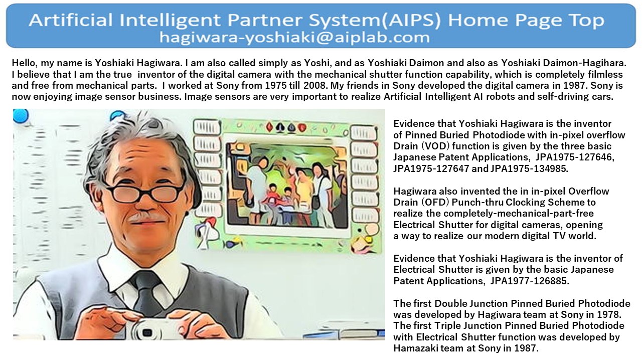
“Story of Image Sensor, Intelligent Electric Eye” TOP
**************************************************

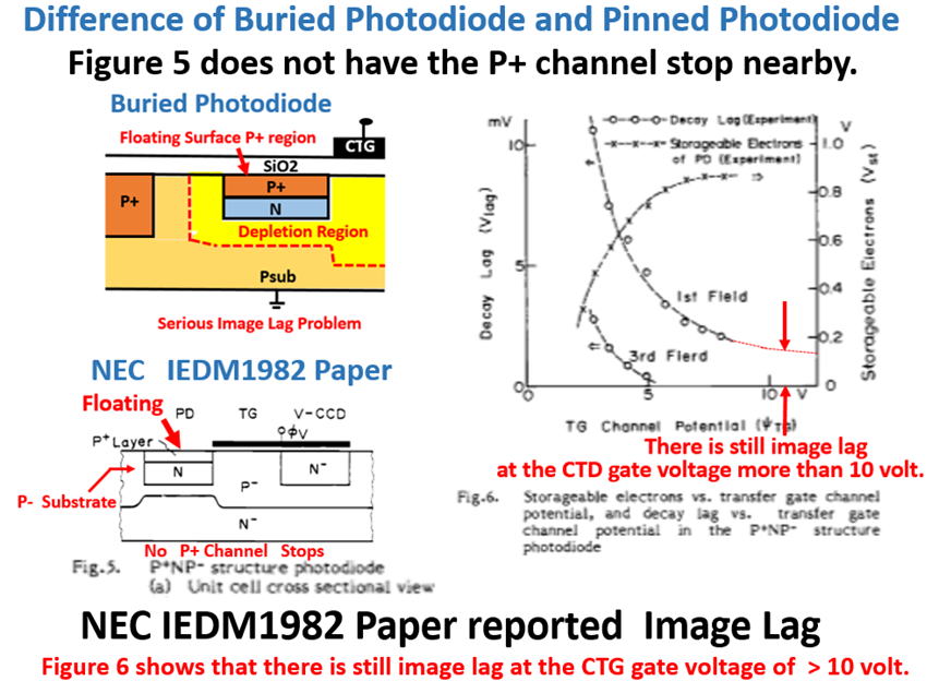
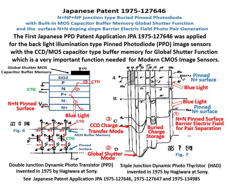
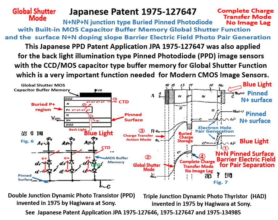
● Image Sensor は 大きく、2つの部品で構成されます。

    1 つは 受光素子です。もう 1 つは 電荷転送装置です。

      CCD型電荷転送装置が昔は脚光を浴びていましたが、
       現在では、CMOS 型電荷転送装置が 主流です。

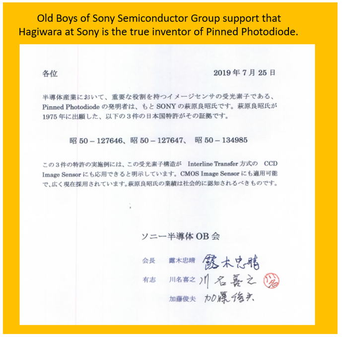
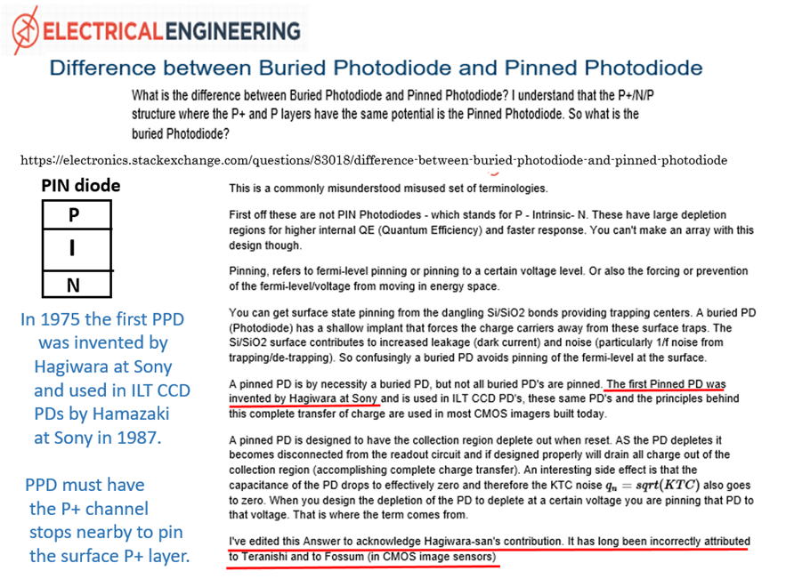
しかし、受光素子は、1975年に もと SONYの萩原が発明したものが
今でも 採用されています。受光面のP+層がピン止め電圧固定された、
P+NP接合型の Dynamic Photo Transistor 型の受光素子です。

 Buried Pinned Photodiode といいます。 

 単純な Photodiode ではありません。

Dynamic Photo Transistor には、いろいろな有効な動作があります。


もと SONYの萩原良昭は、基板に P+NP 型 dynamic photo transistor
を形成して、実効的に、P+NPNsub 接合型の受光素子を発明しました。

この P+NPNsub 接合型 Dynamic Thyristor 型受光素子には、
Punch Thru 動作など、いろいろな有効な機能があります。

縦型の Overflow Drain (VOD)機能付きで、かつ、残像のない 
特徴が不可欠である、電子 shutter 機能を実現しました。


萩原が1975年に発明した、P+NPNsub 接合型受光素子のみが
電子 shutter 機能が 可能です。この電子 shutter 機能が、
今の、デジカメの、高速アクション映像を可能にしました。


*********************************************************************


http://www.aiplab.com/index_Page003_Invention_of_Pinned_Photodiode_in_1975.html

*********************************************************************


Yoshiaki Hagiwara wrote a book on
"the World of Artificial Intelligent Digital Circuits",
which is important and needed to built
the intelligent image sensor systems.

ISBM978-4-88359-339-2
Hard Cover, 460 page,
\ 9000 Japanese Yen + tax

If you are interestied in the book, Please visit

https://www.seizansha.co.jp/ISBN/ISBN978-4-88359-339-2.html

https://www.seizasha.co.jp/


*
************************************************************
The following four Japanese Patent Applications explained that
Hagiwara invented Pinned Photodiode with VOD function in 1975.
 index001_Image_Sensor_1975_1977_and_2014_Patents.html
*************************************************************
 index002_Facts_on_Invention_of_Pinned_Photodiode.html
 index003_Hagiwara_Publication_List.html
 index004_My_Wonderful_Memory_Pictures.html
 index005_Image_Sensor_Story_by_Hagiwara.html
*************************************************************

********************************************************
hagiwara-yoshiaki@aiplab.com http://www.aiplab.com/

hagiwara@ssis.or.jp http://www.ssis.or.jp/en/index.html
********************************************************

******************************
Return to Top Page
 http://www.aiplab.com/

*********************************