


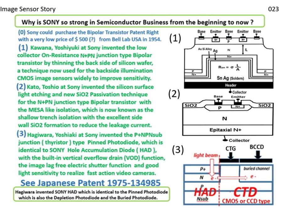
***********************************************
******
豆知識 <-- 萩原良昭が知らなかった言葉です(苦笑)。
******
岳樺(ダケカンバ)
木犀(もくせい)
曼珠沙華(マンジュシャゲ)
欅(ケヤキ)
凭れる(もたれる)
繁(しげ)
諍(いさか)う
言争(いいあらがう)
ひぐらし
ユキノシタ(雪の下)の花言葉とは?
切岸(きりぎし)とは?
莪 とは ?
蓼莪之詩 (りくがのし) とは ?
梢(こずえ) とは?
*************************************
+++++++++++++++++++++++++++++++++++++++++++++++++++++++++++++
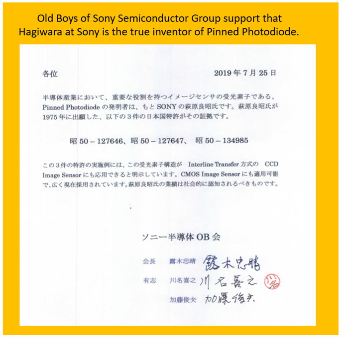
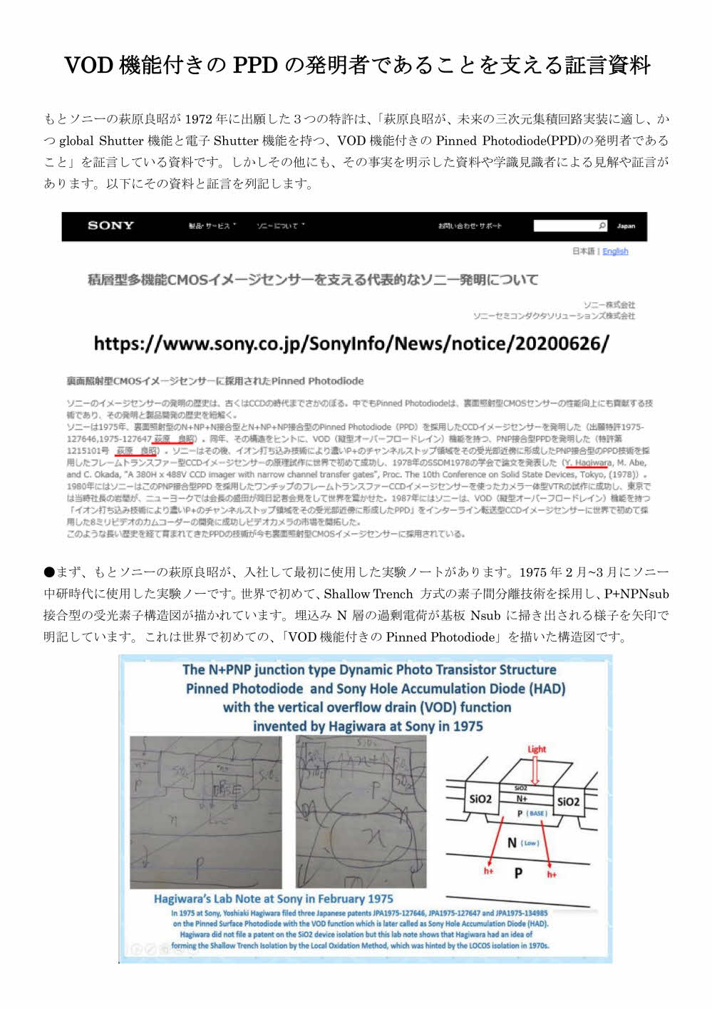
JPG001_Sony_Semiconductor_Gp_OBs_support_Hagiwara_1975_PPD_invention
http://www.aiplab.com/Sony_Semiconductor_Gp_OBs_support_Hagiwara_PPD_invention.jpg
JPG002_Sony_acknowledged_that_Hagiwara_invented_PPD_with_VOD_for_Electric_Shutter_Function
http://www.aiplab.com/Image_Sensor_Story_07.jpg
JPG003_Hagiwara_drew_the_Triple_Junction_Type_Pinned_Photodiode_in_his_1975_Lab_Note
http://www.aiplab.com/NPNP_junction_Pinned_Photodiode_in_1975_by_Hagiwara_A.jpg

JPG004_Hagiwara_drew_the_Triple_Junction_Type_Pinned_Photodiode_in_his_1975_Lab_Note
http://www.aiplab.com/image3A_Hagiwara_at_Sony_invented_Pinned_Photodiode_in_1975.jpg
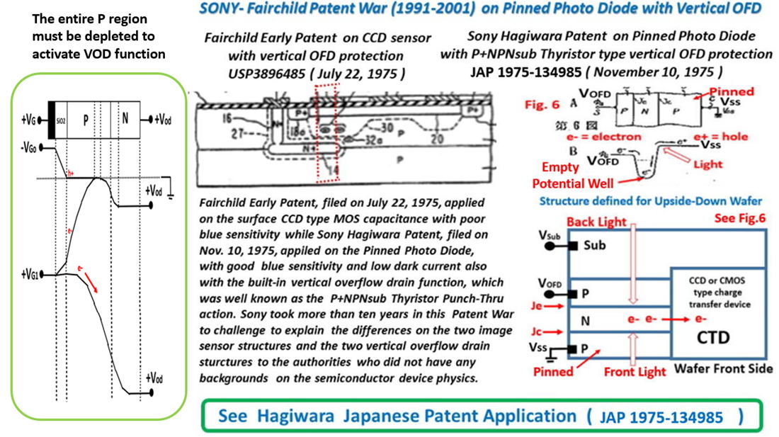
JPG005_Fairchild_Attacked_Sony_but_Hagiwara_defended_Sony_with_Hagiwara_1975_PPD_Patent
http://www.aiplab.com/End_of_Sony_Fairchild_Patent_War.jpg
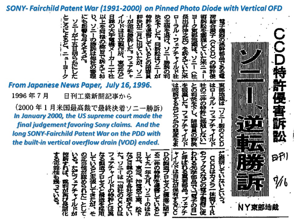
JPG006_Fairchild_Attacked_Sony_but_Hagiwara_defended_Sony_with_Hagiwara_1975_PPD_Patent
http://www.aiplab.com/SONY_Fairchild_Patent_War.jpg
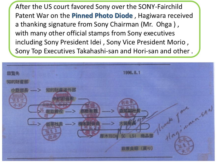
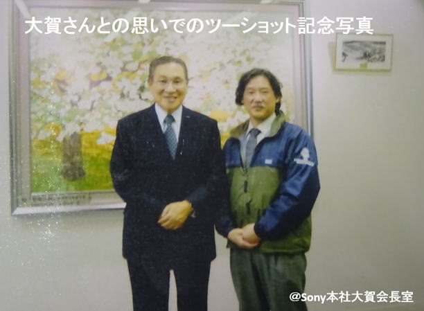
JPG007_Hagiwara_received_Thanking_Words_from_Sony_Chairman_Ohga_and_President_Idei.
http://www.aiplab.com/Thank_You_Note_from_President_Ohga.jpg
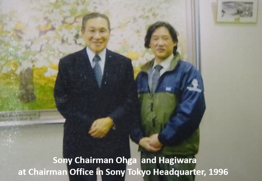
JPG008_Sony_Chairman_Ohga_and_Hagiwara_shared_a_happy_time_in_Sony_Chairman_Office
http://www.aiplab.com/SONY_Ohga_Chairman_and_Hagiwara_1996.jpg
JPG009_Sony_President_Idei_awarded_Hagiwara_the_Bset_Patent_Prize_on_the_Electrical_Shutter_Patent
http://www.aiplab.com/Sony_patent_Award_on_Electric_Shutter_HAD.jpg
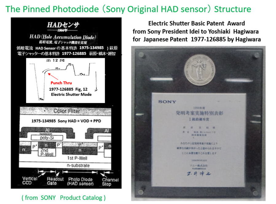
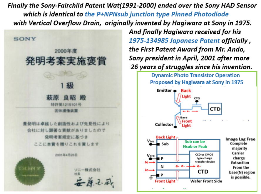
JPG010_Sony_President_Ando_awarded_Hagiwara_the_First_Patent_Prize_on_Pinned_Photodiode_(HAD)_Patent
http://www.aiplab.com/Sony_Patent_Award_on_Pinned_Phtodiode.jpg
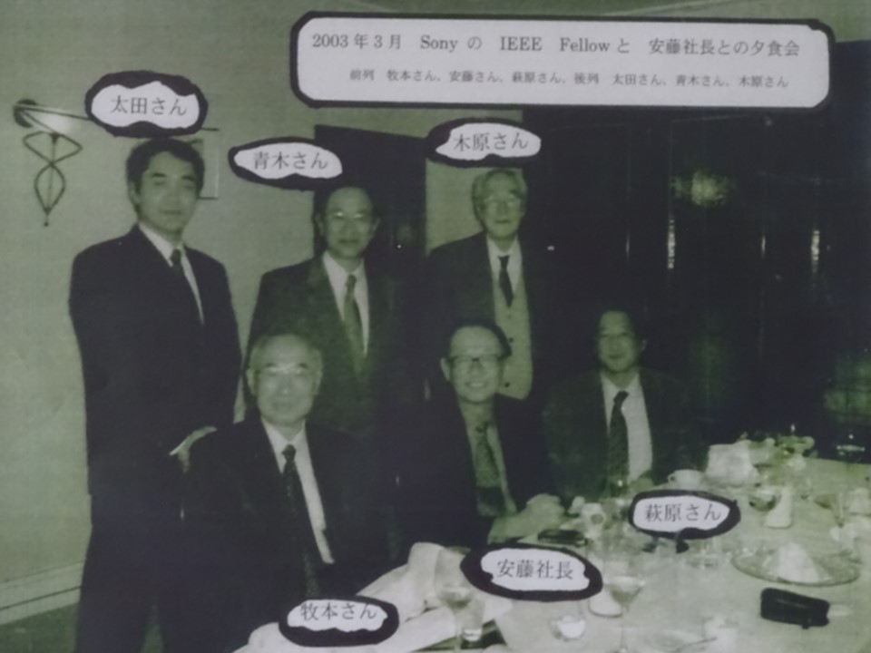
JPG011_Sony_President_Ando_and_Hagiwara_shared_a_happy_time_with_Sony/IEEE_Fellows.
http://www.aiplab.com/SONY_Ando_President_and_Hagiwara_2003.jpg
JPG012_Semiconductor_History_Museum_of_Japan_also_supoorts__Hagiwara_1975_PPD_invention
http://www.aiplab.com/image3J_Hagiwara_at_Sony_invented_Pinned_Photodiode_in_1975.jpg
JPG013_Semiconductor_History_Museum_of_Japan_also_supoorts__Hagiwara_1975_PPD_invention
http://www.aiplab.com/image3E_Hagiwara_at_Sony_invented_Pinned_Photodiode_in_1975.jpg
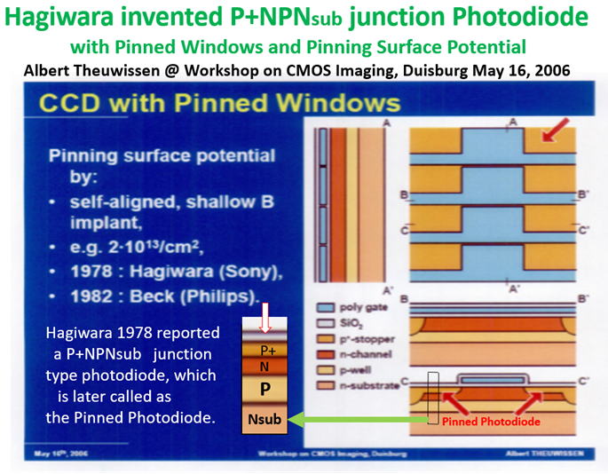
JPG014_Prof._Albert_Theuwissen_(President_of_Internationl_Image_Sensors_Society)_quoted_Hagiwara_1978_work
https://202011282002569657330.onamaeweb.jp/AIPS_Library/AIPS_190712/image208.jpg
JPG016_Prof._Albert_Theuwissen_also_supoorts__Hagiwara_1975_PPD_invention_and_Hagiwara_1978_PPD_develpment_works
http://www.aiplab.com/E-mail_communication_with_Albert_san_2018_07_10A.jpg
JPG017_Prof._Albert_Theuwissen_also_supoorts__Hagiwara_1975_PPD_invention_and_Hagiwara_1978_PPD_develpment_works
http://www.aiplab.com/E-mail_communication_with_Albert_san_2018_07_10B.jpg
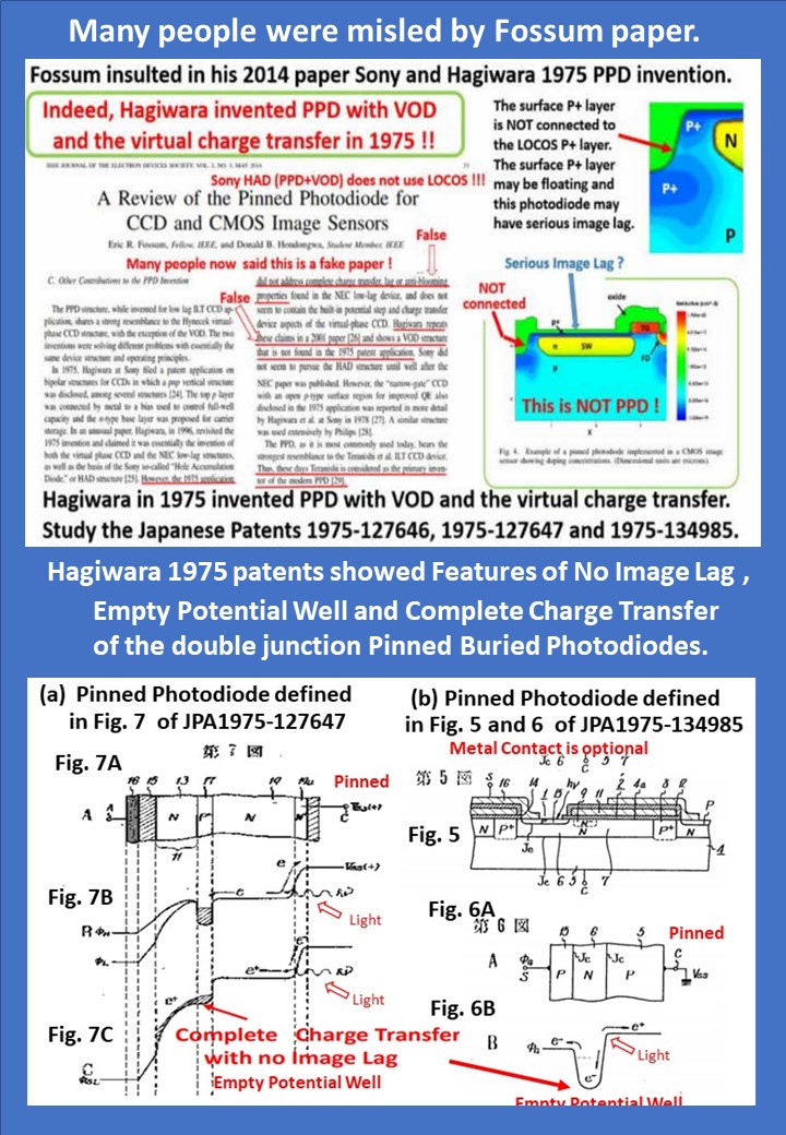
JPG018_Fossum_insulted_Hagiwara_1975_invention_and_Sony_Hole_Accumlation_Diode_(HAD)_invention.
http://www.aiplab.com/image3D_Hagiwara_at_Sony_invented_Pinned_Photodiode_in_1975.jpg
JPG019_the_WEB_site_comment supports_that_Teranishi's PPD and Fossum's
CMOS are fakes.
http://www.aiplab.com/Difference_of_Pinned_Photodiode_and_Buried_Photodiode.jpg
JPG020_The_WEB_site_of_Innovation100_does_not_describe_the_truth_about_PPD_and_VOD_inventions.
http://www.aiplab.com/Misunderstanding_on_Pinned_Photodiode_History.jpg
JPG021_All_Misunderstandings_on_PPD_inventions_should_be_clearified_by_Hagiwara_1975_PPD_Patent_Applications.
http://www.aiplab.com/Image_Sensor_Story_14.jpg
JPG022_NEC(Teranishi)_did_not_invented_PPD_in_1979_and_the_IEDM1982_Teranishi_Photodiode_was_NOT_PPD
http://www.aiplab.com/image3B_Hagiwara_at_Sony_invented_Pinned_Photodiode_in_1975.jpg
JPG023_Difference_of_Buried_Photodiode_and_Pinned_Photodiode_must_be_understood_clearly.
http://www.aiplab.com/Difference_of_Pinned_Photodiode_and_Buried_Photodiode_1.jpg
JPG024_Difference_of_Buried_Photodiode_and_Pinned_Photodiode_must_be_understood_clearly.
http://www.aiplab.com/Difference_of_Buried_Photodiode_and_Pinned_Photodiode_1.jpg
JPG025_Pinned_Photodiode_must_have_Adjacent_Channel_Stops_nearby_
................in order to_pin_the_surface_ P+_hole_accumulation_layer....
http://www.aiplab.com/Hagiwara_invented_PPD_and_Virtual_Charge_Transfer.jpg
![]()
JPG025_Hagiwara_invented_in_1975_the_P+NPsub double_junction_dynamic_photo_transistor_
..............with...1) Very Excellent Short Wave Blue Light Sensitivity,
........................2) Comptete Charge Transfer Capability with Image
Lag Free Feature
........................3) and Pinned Surface P+ Hole Accumulation with No Surface Dark Current.
.........and_Hagiwara_also_invented_in_1975_the_triple_junction_dynamic_photo_thyristor
..............with...4) Completely Charge Draining Vertical Overflow Drain
(VOD) function
............................... needed in the completely mechanical-free electrical shutter function
................................ for the modern Filmless and Completely Electrical Image Sensors.
http://www.aiplab.com/Difference_of_Static_and_Dynamic_Photo_Transistor.jpg
![]()
JPG026_Hagiwara_invented_the_Virtual_Phase_Charge_Transfer_in_1975
http://www.aiplab.com/Hagiwara_invented_PPD_and_Virtual_Charge_Transfer_in_1975_S01.jpg
![]()
JPG027_Hagiwara_invented_the_Virtual_Phase_Charge_Transfer_in_1975
http://www.aiplab.com/Hagiwara_invented_PPD_and_Virtual_Charge_Transfer_in_1975_S02.jpg
![]()
JPG028_Hagiwara_invented_the_Virtual_Phase_Charge_Transfer_in_1975
http://www.aiplab.com/Hagiwara_invented_PPD_and_Virtual_Charge_Transfer_in_1975_S03.jpg
![]()
JPG029_Hagiwara_invented_the_Virtual_Phase_Charge_Transfer_in_1975
http://www.aiplab.com/Hagiwara_invented_PPD_and_Virtual_Charge_Transfer_in_1975_S04.jpg
![]()
JPG030_Hagiwara_invented_the_Virtual_Phase_Charge_Transfer_in_1975
http://www.aiplab.com/Hagiwara_invented_PPD_and_Virtual_Charge_Transfer_in_1975_S05.jpg
![]()
JPG031_Hagiwara_invented_the_Virtual_Phase_Charge_Transfer_in_1975
http://www.aiplab.com/Hagiwara_invented_PPD_and_Virtual_Charge_Transfer_in_1975_S06.jpg
![]()
JPG032_Hagiwara_invented_the_Virtual_Phase_Charge_Transfer_in_1975
http://www.aiplab.com/Hagiwara_invented_PPD_and_Virtual_Charge_Transfer_in_1975_S07.jpg
![]()
JPG033_Hagiwara_invented_the_Virtual_Phase_Charge_Transfer_in_1975
http://www.aiplab.com/Hagiwara_invented_PPD_and_Virtual_Charge_Transfer_in_1975_S08.jpg
![]()
JPG034_Hagiwara_invented_the_Virtual_Phase_Charge_Transfer_in_1975
http://www.aiplab.com/P1996_no_image_lag_pinned_photo-diode_invented_in_1975_by_Hagiwara.jpg
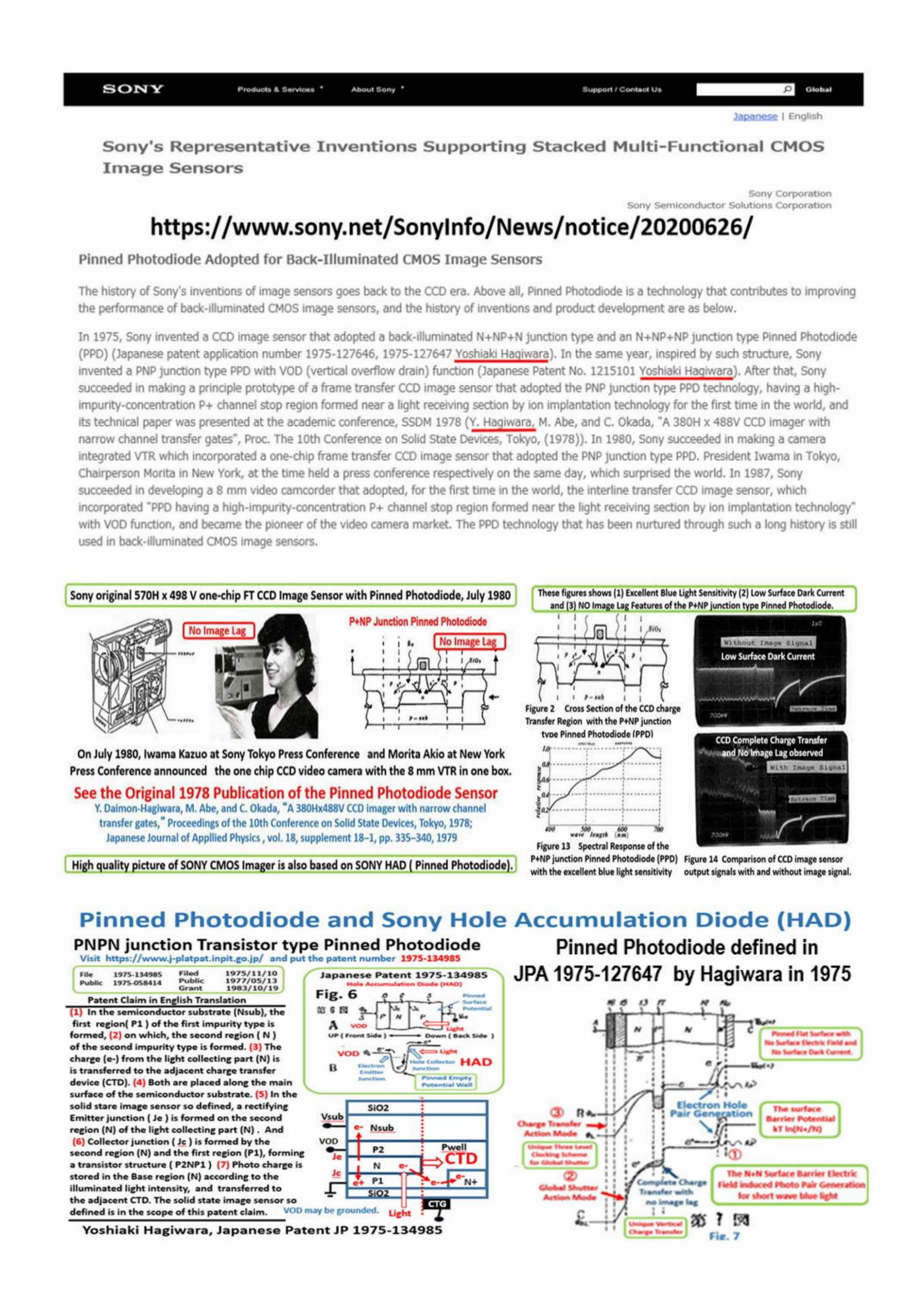
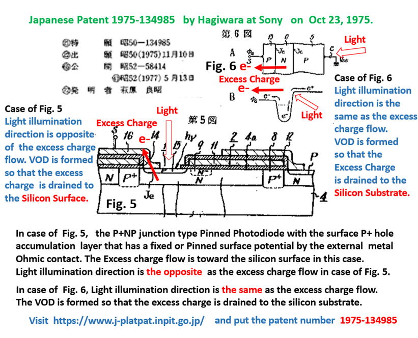
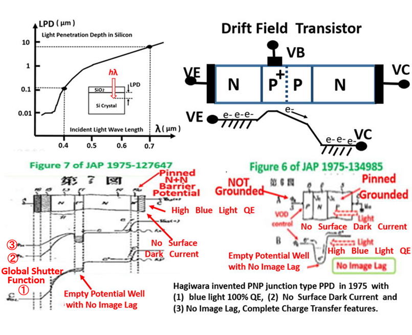
JPG035_Hagiwara_invented_in_1975_the_double_junction_dynamic_photo_transistor_and_the_triple_junction_dynamic_photo_thyristor
http://www.aiplab.com/JP1975-134985_Patent_Claims_in_English_Translation.jpg
![]()
JPG036_Hagiwara_invented_in_1975_the_double_junction_dynamic_photo_transistor_with_no_image_lag_feature_and_VOD_function
http://www.aiplab.com/Two_type_of_VOD_in_JP1975-134985.jpg
JPG037_Most_important_Contribution_of_Hagiwsara_1975_PPD_invention_was_the_short_wave_blue_light_Sensitivity
http://www.aiplab.com/What_is_True_Pinned_Photodiode.jpg
JPG038_Most_important_Contribution_of_Hagiwsara_1975_PPD_invention_was_the_short_wave_blue_light_Sensitivity
http://www.aiplab.com/Pinned_Photodiode_Drift_Field_Trasistor.jpg
JPG039_Most_important_Contribution_of_Hagiwsara_1975_PPD_invention_was_the_short_wave_blue_light_Sensitivity
http://www.aiplab.com/Pinned_Photodiode_Reported_in_Hagiwara_SSDM1978_Paper.jpg
+++++++++++++++++++++++++++++++++++++++++++++++++++++++++++++++++++++++++
+++++++++++++++++++++++++++++++++++++++++++++++++++++++++++++
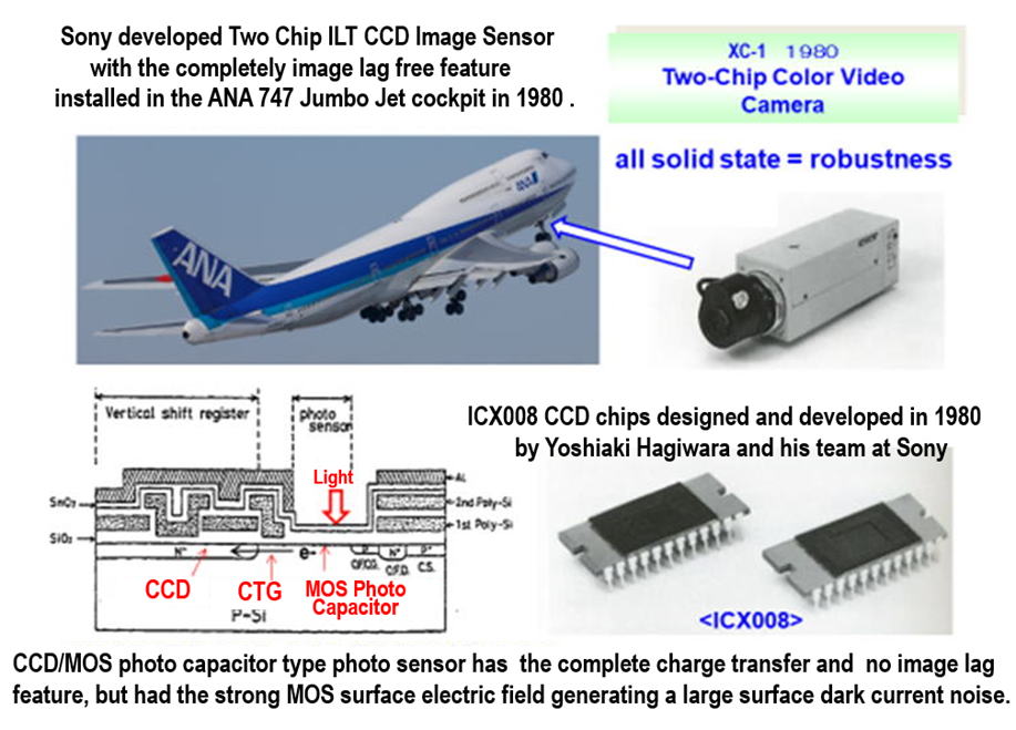
JPG040_Hagiwara _also_designed_and_developed the_CCD/MOS_Photo_Capacitor_type
.................. Two_Chip_Interline_Transfer (ILT)_type_CCD_Image_Sensor_in_1980,
................... which has the CCD/MOS type complete charge transfer
function
................... with the excellent image lag free feature for fast
action pictures
..................... and used in the ANA 747 JumboJet Cockpits.
JPG040_Image_Sensor_Story_08.jpg
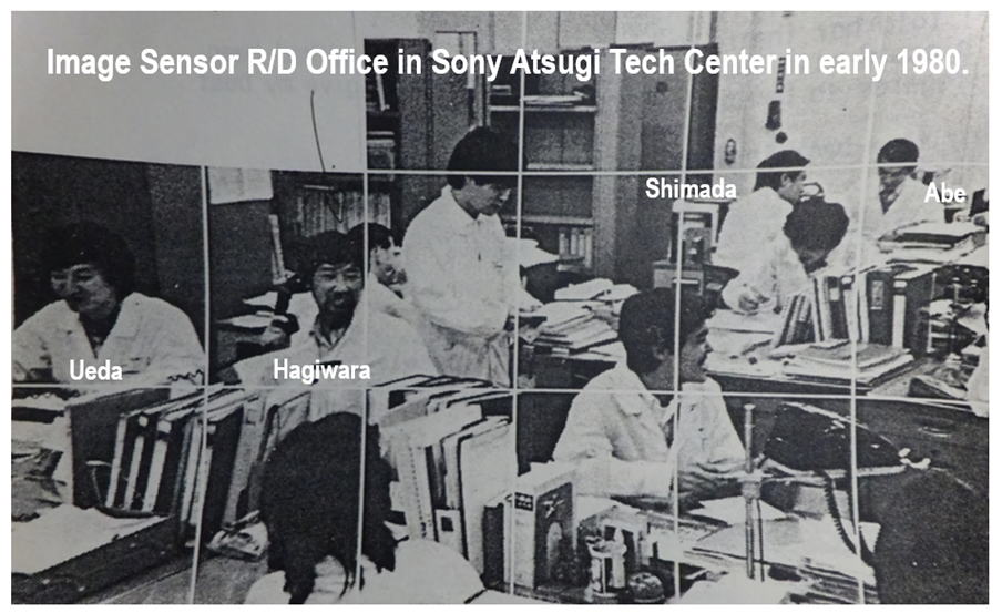
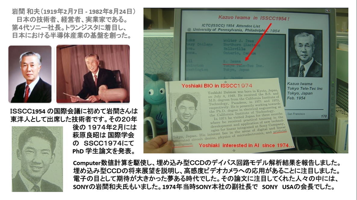
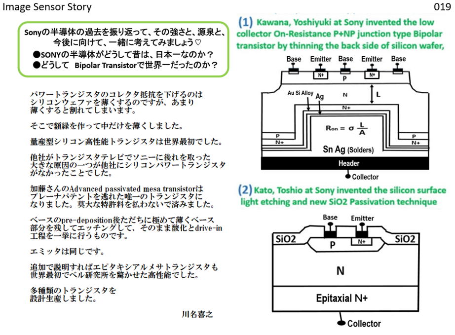
Sony EX-President Kazuo Iwama attended the First IEEE ISSCC1954conference,
was the leader and the father of Sony's Devlopment Eforts for Bipolar Transistor
and Sony Portable Transistor Radios, and is now considered to be the Father
of
Sony's Development Efforts of CCD and CMOS Image Sensor Products. Hagiwara
published his PhD thesis paper on the charge transfer analysis of the Buried
Channel CCD image sensors in the ISSCC1974 conference. One year later,
Hagiwara joined Sony on February 1975 and worked for developping CCD image
sensors at Sony Central Research Center in Yokohama, Japan.
JPG041_Iwama_Kasuo_in_ISSCC1954.jpg
Hagiwara served in various international technical conference committees including ISSCC.
JPG042_ISSCC2003_Executive_Committee_Contribution_Award.jpg

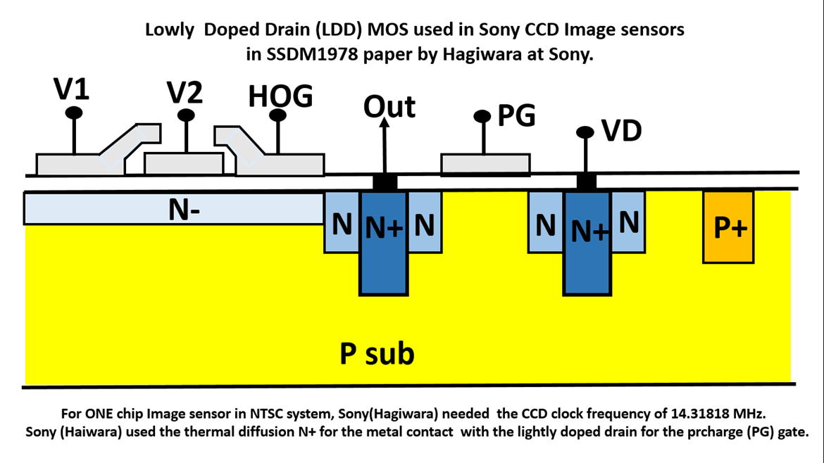
Hagiwara did not publish various important suttle techical items,
but they helped a lot to produce high performance image sensors..
JPG043_Lightly_Doped_Drain_used_in_Sony_1978_Process.jpg
JPG044_Memory_of_Friends_in_Sony_Kumamoto_Tech.jpg
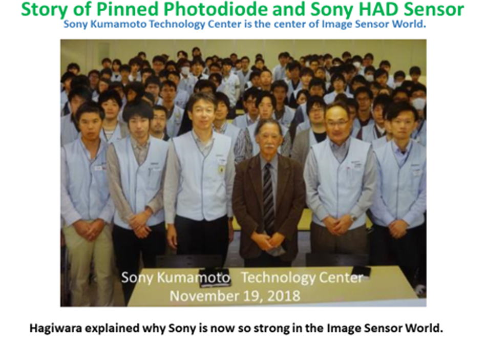
JPG045_Memory_Sony_Kumamoto_tech.jpg
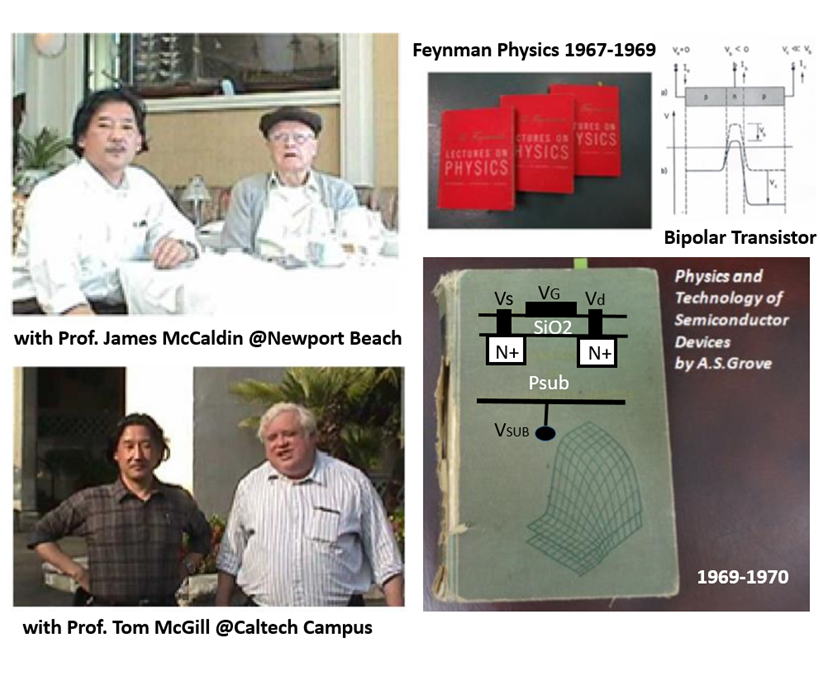
Hagiwara owes so much to Prof. James McCaldin, Prof. T.C. McGill
and Prof.C.A. Mead at California Institute for Technology (Caltech).
Hagiwara studied the bipolar transistor structure and the operational
physics from the Feyman Lecture Book when he was the seoncd year
of his undergradute student life in Caltech, Pasadena in 1968 at age 20.
JPG046_Memory1998_Prof_T_C_McGill_and_Prof_James_McCaldin.jpg
JPG047_My_Lief_Long_Dream__Hagiwara_Yoshiaki.jpg
+++++++++++++++++++++++++++++++++++++++++++++++++++++++++++++
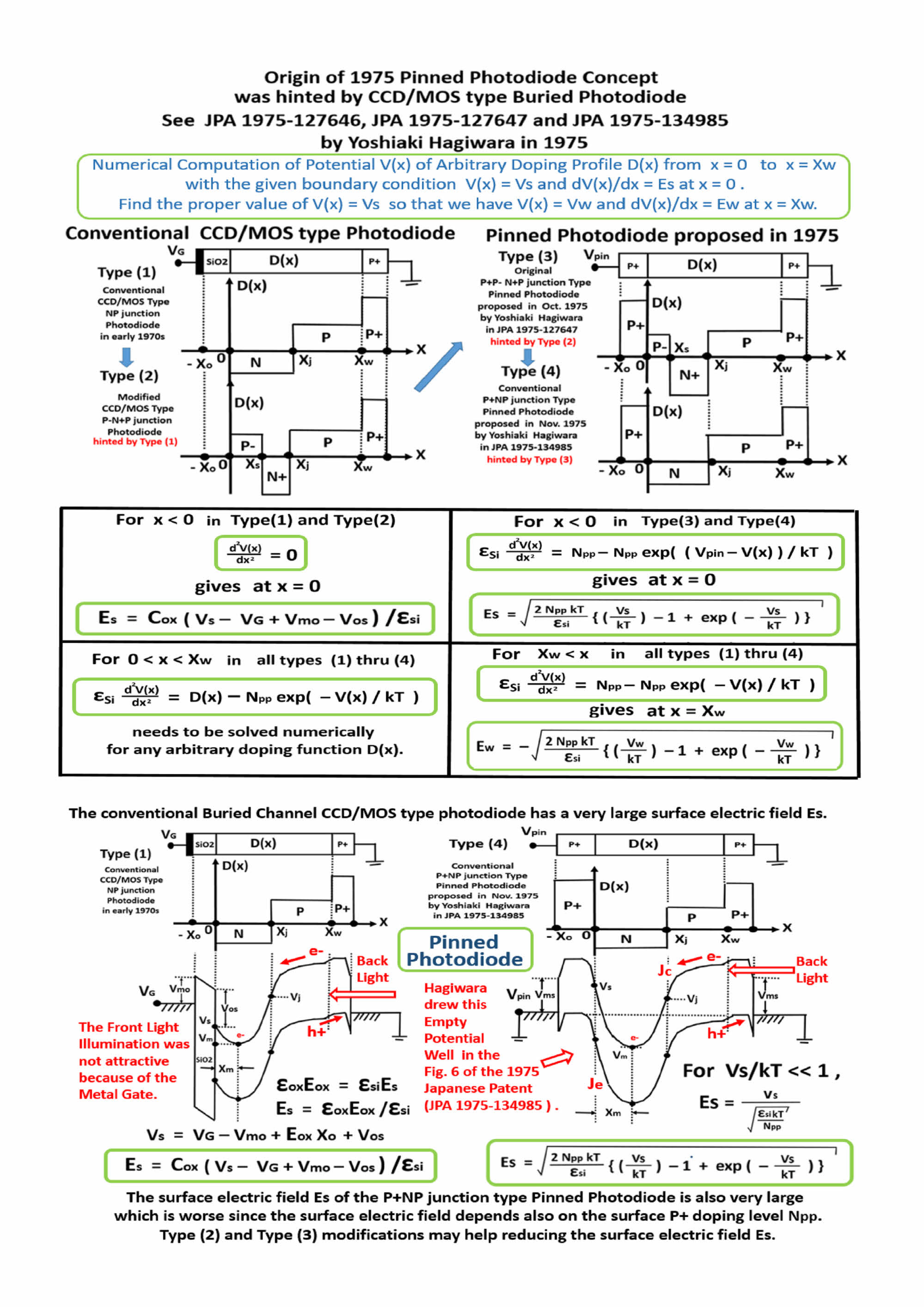
JPG048_Origin_of_1975_Concept_of_Pinned_Photodiode_.jpg
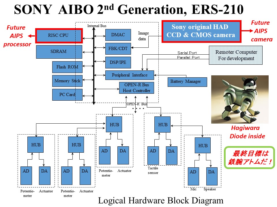
JPG049_P2001_ESSCIRC2001_SONY_AIBO.jpg
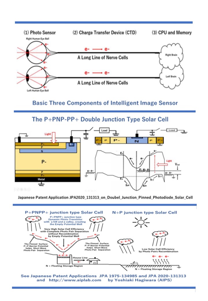
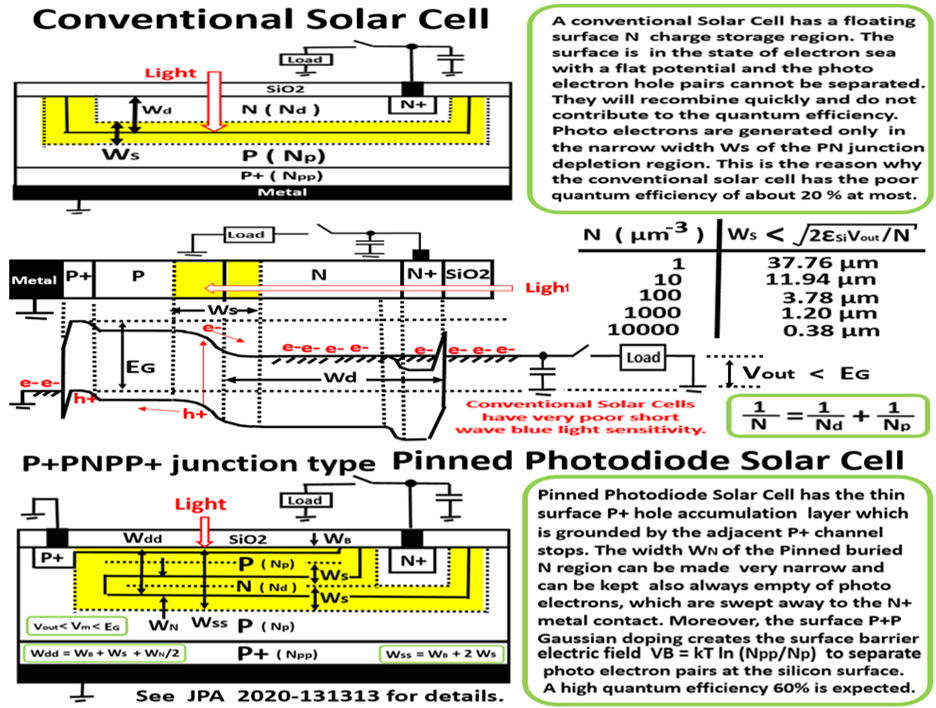
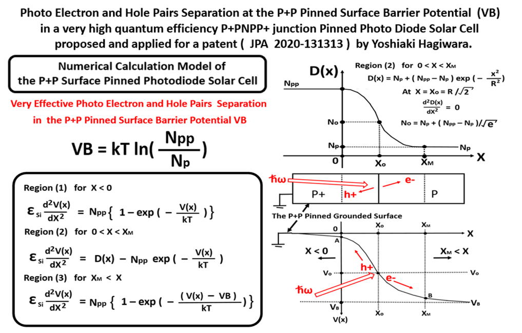
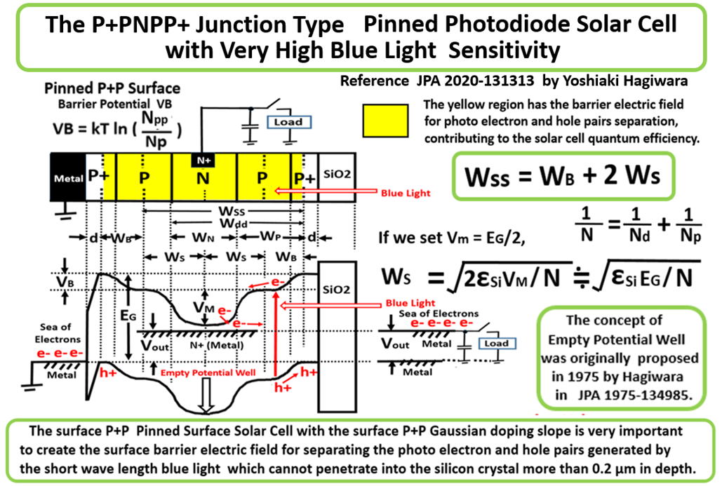
JPG050_P2020_Minimum_Potential_and_Width_of_Solar_Cell.jpg
JPG051_Pinne_Photodiode_Solar_Cell.jpg
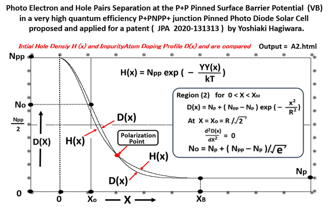
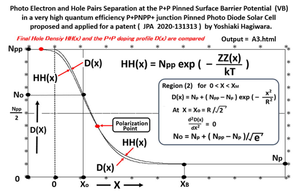
JPG052_Pinned_Photodiode_Surface_Barrier_Potential.jpg
+++++++++++++++++++++++++++++++++++++++++++++++++++++++++++++
JPG053_Pinned_Photodiode_Surface_Barrier_Potential_1.jpg

JPG054_Pinned_Photodiode_Surface_Barrier_Potential_2.jpg
JPG055_Pinned_Photodiode_Surface_Barrier_Potential_3.jpg
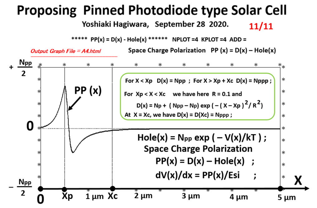
JPG056_Proposal_of_Pinned_Photodiode_type_Solar_Cell.jpg
JPG057_Proposal_of_Pinned_Photodiode_type_Solar_Cell_01.jpg
JPG058_Proposal_of_Pinned_Photodiode_type_Solar_Cell_02.jpg
JPG059_Proposal_of_Pinned_Photodiode_type_Solar_Cell_03.jpg
JPG061_Proposal_of_Pinned_Photodiode_type_Solar_Cell_04.jpg
JPG062_Proposal_of_Pinned_Photodiode_type_Solar_Cell_05.jpg
JPG063_Proposal_of_Pinned_Photodiode_type_Solar_Cell_06.jpg

JPG064_Proposal_of_Pinned_Photodiode_type_Solar_Cell_07.jpg

JPG065_Proposal_of_Pinned_Photodiode_type_Solar_Cell_09.jpg
JPG066_Proposal_of_Pinned_Photodiode_type_Solar_Cell_10.jpg
JPG067_Proposal_of_Pinned_Photodiode_type_Solar_Cell_11.jpg
JPG068_PS3_Cell_Proceesor_Sony_Team_Award.jpg

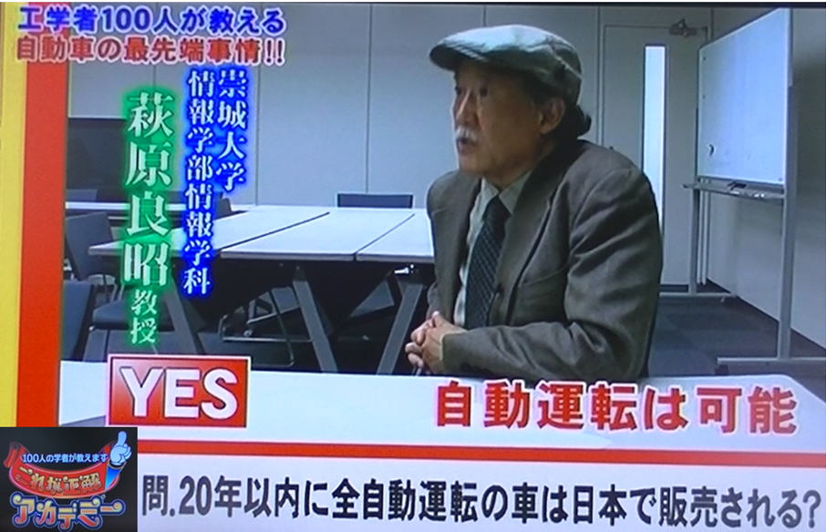
JPG069_Self_Driving_Car_TV_interview_2013.jpg
JPG070_Simple_PN_junction_Solar_Cell.jpg
JPG071_Slide019A_Sony_Atsugi_Tech_2020_07_10.jpg
JPG072_Slide023A_Sony_Atsugi_Tech_2020_07_10.jpg
JPG073_Solar_Cell_with_High_Blue_Light_Sensitivity.jpg
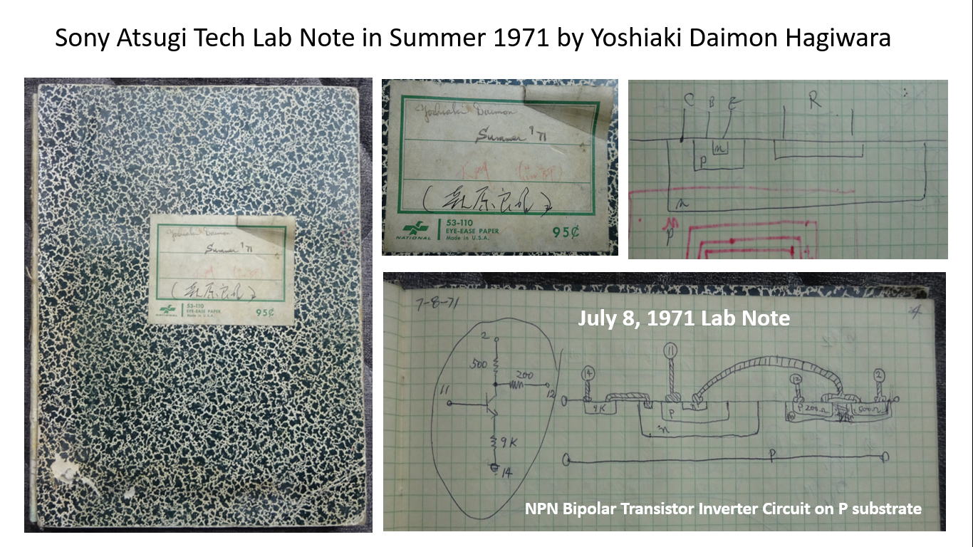
JPG074_Sony_Atsugi_Tech_Lab_Note_in_Summer_1971_by_Yoshiaki_Daimon_Hagiwara.jpg
JPG075_Sony_Kodak_Patent_Agreement.jpg
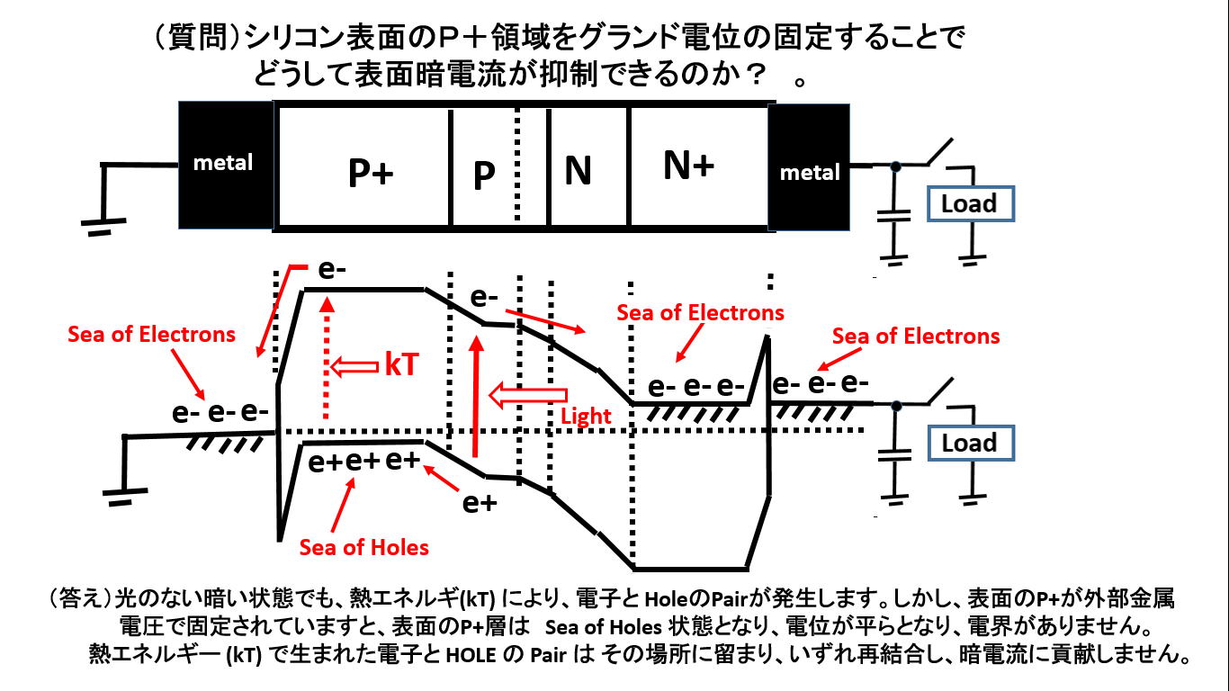
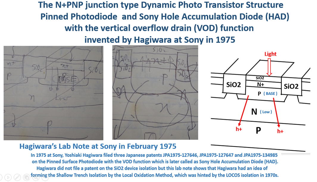
Hagiwara invented in 1975 the double junction type dynamic photo transistor
which was
later called as Pinned Photodiode by Kodak in IEDM1984, and also Hagiwara invented
in 1975 the triple junction type dynamic photo thyristor, which as later called in 1987
as Sony's Hole Accumulation Diode (HAD), the NPNP junction thyristor type photodiode ,
with the punch thru operation which is applied to achieve the vertical overflow drain
and the electrical shutter functions for fact action movie camera pictures with the
completely image lag free and mecahnical parts free features for the Filmless
society.
JPG076_Three_types_of_in_pixel_Vertical_Overflow_Drain_VOD.jpg
![]()
+++++++++++++++++++++++++++++++++++++++++++++++++++++++++++++
JPG001_Sony_Semiconductor_Gp_OBs_support_Hagiwara_1975_PPD_invention
http://www.aiplab.com/Sony_Semiconductor_Gp_OBs_support_Hagiwara_PPD_invention.jpg
JPG002_Sony_acknowledged_that_Hagiwara_invented_PPD_with_VOD_for_Electric_Shutter_Function
http://www.aiplab.com/Image_Sensor_Story_07.jpg
JPG003_Hagiwara_drew_the_Triple_Junction_Type_Pinned_Photodiode_in_his_1975_Lab_Note
http://www.aiplab.com/NPNP_junction_Pinned_Photodiode_in_1975_by_Hagiwara_A.jpg
JPG004_Hagiwara_drew_the_Triple_Junction_Type_Pinned_Photodiode_in_his_1975_Lab_Note
http://www.aiplab.com/image3A_Hagiwara_at_Sony_invented_Pinned_Photodiode_in_1975.jpg
JPG005_Fairchild_Attacked_Sony_but_Hagiwara_defended_Sony_with_Hagiwara_1975_PPD_Patent
http://www.aiplab.com/End_of_Sony_Fairchild_Patent_War.jpg
JPG006_Fairchild_Attacked_Sony_but_Hagiwara_defended_Sony_with_Hagiwara_1975_PPD_Patent
http://www.aiplab.com/SONY_Fairchild_Patent_War.jpg
JPG007_Hagiwara_received_Thanking_Words_from_Sony_Chairman_Ohga_and_President_Idei.
http://www.aiplab.com/Thank_You_Note_from_President_Ohga.jpg
JPG008_Sony_Chairman_Ohga_and_Hagiwara_shared_a_happy_time_in_Sony_Chairman_Office
http://www.aiplab.com/SONY_Ohga_Chairman_and_Hagiwara_1996.jpg
JPG009_Sony_President_Idei_awarded_Hagiwara_the_Bset_Patent_Prize_on_the_Electrical_Shutter_Patent
http://www.aiplab.com/Sony_patent_Award_on_Electric_Shutter_HAD.jpg
JPG010_Sony_President_Ando_awarded_Hagiwara_the_First_Patent_Prize_on_Pinned_Photodiode_(HAD)_Patent
http://www.aiplab.com/Sony_Patent_Award_on_Pinned_Phtodiode.jpg
JPG011_Sony_President_Ando_and_Hagiwara_shared_a_happy_time_with_Sony/IEEE_Fellows.
http://www.aiplab.com/SONY_Ando_President_and_Hagiwara_2003.jpg
JPG012_Semiconductor_History_Museum_of_Japan_also_supoorts__Hagiwara_1975_PPD_invention
http://www.aiplab.com/image3J_Hagiwara_at_Sony_invented_Pinned_Photodiode_in_1975.jpg
JPG013_Semiconductor_History_Museum_of_Japan_also_supoorts__Hagiwara_1975_PPD_invention
http://www.aiplab.com/image3E_Hagiwara_at_Sony_invented_Pinned_Photodiode_in_1975.jpg
JPG014_Prof._Albert_Theuwissen_(President_of_Internationl_Image_Sensors_Society)_quoted_Hagiwara_1978_work
https://202011282002569657330.onamaeweb.jp/AIPS_Library/AIPS_190712/image208.jpg
JPG016_Prof._Albert_Theuwissen_also_supoorts__Hagiwara_1975_PPD_invention_and_Hagiwara_1978_PPD_develpment_works
http://www.aiplab.com/E-mail_communication_with_Albert_san_2018_07_10A.jpg
JPG017_Prof._Albert_Theuwissen_also_supoorts__Hagiwara_1975_PPD_invention_and_Hagiwara_1978_PPD_develpment_works
http://www.aiplab.com/E-mail_communication_with_Albert_san_2018_07_10B.jpg
JPG018_Fossum_insulted_Hagiwara_1975_invention_and_Sony_Hole_Accumlation_Diode_(HAD)_invention.
http://www.aiplab.com/image3D_Hagiwara_at_Sony_invented_Pinned_Photodiode_in_1975.jpg
JPG019_the_WEB_site_comment supports_that_Teranishi's PPD and Fossum's
CMOS are fakes.
http://www.aiplab.com/Difference_of_Pinned_Photodiode_and_Buried_Photodiode.jpg
JPG020_The_WEB_site_of_Innovation100_does_not_describe_the_truth_about_PPD_and_VOD_inventions.
http://www.aiplab.com/Misunderstanding_on_Pinned_Photodiode_History.jpg
JPG021_All_Misunderstandings_on_PPD_inventions_should_be_clearified_by_Hagiwara_1975_PPD_Patent_Applications.
http://www.aiplab.com/Image_Sensor_Story_14.jpg
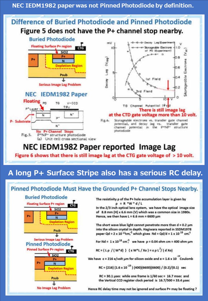
JPG022_NEC(Teranishi)_did_not_invented_PPD_in_1979_and_the_IEDM1982_Teranishi_Photodiode_was_NOT_PPD
http://www.aiplab.com/image3B_Hagiwara_at_Sony_invented_Pinned_Photodiode_in_1975.jpg
JPG023_Difference_of_Buried_Photodiode_and_Pinned_Photodiode_must_be_understood_clearly.
http://www.aiplab.com/Difference_of_Pinned_Photodiode_and_Buried_Photodiode_1.jpg
JPG024_Difference_of_Buried_Photodiode_and_Pinned_Photodiode_must_be_understood_clearly.
http://www.aiplab.com/Difference_of_Buried_Photodiode_and_Pinned_Photodiode_1.jpg
JPG025_Pinned_Photodiode_must_have_Adjacent_Channel_Stops_nearby_
................in order to_pin_the_surface_ P+_hole_accumulation_layer....
http://www.aiplab.com/Hagiwara_invented_PPD_and_Virtual_Charge_Transfer.jpg
JPG025_Hagiwara_invented_in_1975_the_P+NPsub double_junction_dynamic_photo_transistor_
..............with...1) Very Excellent Short Wave Blue Light Sensitivity,
........................2) Comptete Charge Transfer Capability with Image
Lag Free Feature
........................3) and Pinned Surface P+ Hole Accumulation with No Surface Dark Current.
.........and_Hagiwara_also_invented_in_1975_the_triple_junction_dynamic_photo_thyristor
..............with...4) Completely Charge Draining Vertical Overflow Drain
(VOD) function
............................... needed in the completely mechanical-free electrical shutter function
................................ for the modern Filmless and Completely Electrical Image Sensors.
http://www.aiplab.com/Difference_of_Static_and_Dynamic_Photo_Transistor.jpg
JPG026_Hagiwara_invented_the_Virtual_Phase_Charge_Transfer_in_1975
http://www.aiplab.com/Hagiwara_invented_PPD_and_Virtual_Charge_Transfer_in_1975_S01.jpg
JPG027_Hagiwara_invented_the_Virtual_Phase_Charge_Transfer_in_1975
http://www.aiplab.com/Hagiwara_invented_PPD_and_Virtual_Charge_Transfer_in_1975_S02.jpg
JPG028_Hagiwara_invented_the_Virtual_Phase_Charge_Transfer_in_1975
http://www.aiplab.com/Hagiwara_invented_PPD_and_Virtual_Charge_Transfer_in_1975_S03.jpg
JPG029_Hagiwara_invented_the_Virtual_Phase_Charge_Transfer_in_1975
http://www.aiplab.com/Hagiwara_invented_PPD_and_Virtual_Charge_Transfer_in_1975_S04.jpg
JPG030_Hagiwara_invented_the_Virtual_Phase_Charge_Transfer_in_1975
http://www.aiplab.com/Hagiwara_invented_PPD_and_Virtual_Charge_Transfer_in_1975_S05.jpg
JPG031_Hagiwara_invented_the_Virtual_Phase_Charge_Transfer_in_1975
http://www.aiplab.com/Hagiwara_invented_PPD_and_Virtual_Charge_Transfer_in_1975_S06.jpg
JPG032_Hagiwara_invented_the_Virtual_Phase_Charge_Transfer_in_1975
http://www.aiplab.com/Hagiwara_invented_PPD_and_Virtual_Charge_Transfer_in_1975_S07.jpg
JPG033_Hagiwara_invented_the_Virtual_Phase_Charge_Transfer_in_1975
http://www.aiplab.com/Hagiwara_invented_PPD_and_Virtual_Charge_Transfer_in_1975_S08.jpg
JPG034_Hagiwara_invented_the_Virtual_Phase_Charge_Transfer_in_1975
http://www.aiplab.com/P1996_no_image_lag_pinned_photo-diode_invented_in_1975_by_Hagiwara.jpg
JPG035_Hagiwara_invented_in_1975_the_double_junction_dynamic_photo_transistor_and_the_triple_junction_dynamic_photo_thyristor
http://www.aiplab.com/JP1975-134985_Patent_Claims_in_English_Translation.jpg
JPG036_Hagiwara_invented_in_1975_the_double_junction_dynamic_photo_transistor_with_no_image_lag_feature_and_VOD_function
http://www.aiplab.com/Two_type_of_VOD_in_JP1975-134985.jpg
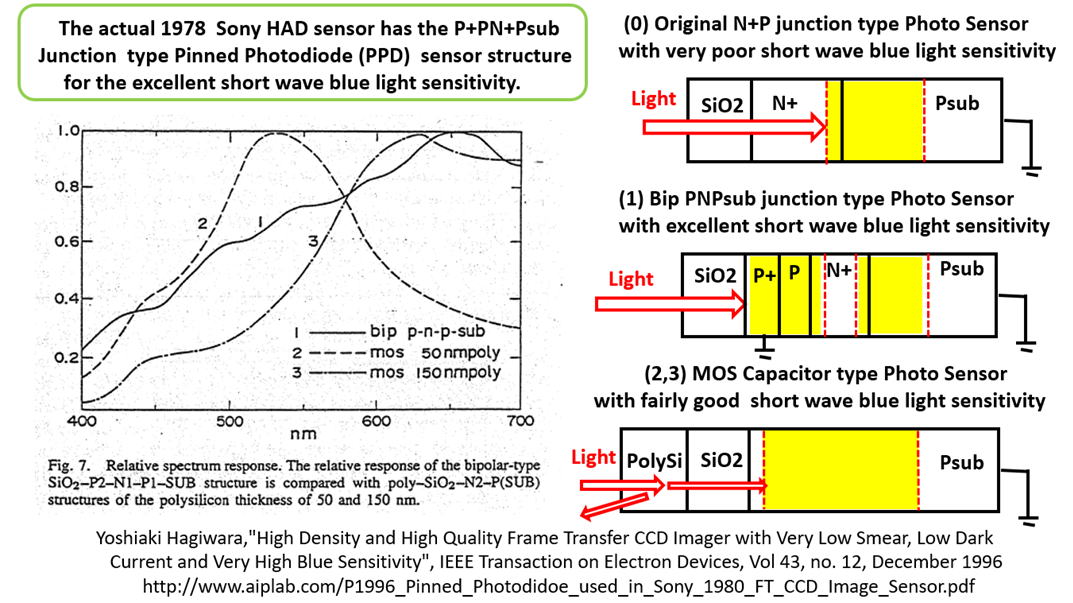
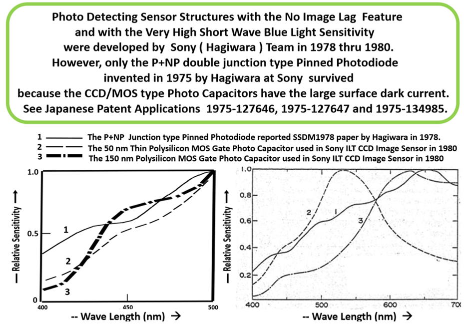
JPG037_Most_important_Contribution_of_Hagiwsara_1975_PPD_invention_was_the_short_wave_blue_light_Sensitivity
http://www.aiplab.com/What_is_True_Pinned_Photodiode.jpg
JPG038_Most_important_Contribution_of_Hagiwsara_1975_PPD_invention_was_the_short_wave_blue_light_Sensitivity
http://www.aiplab.com/Pinned_Photodiode_Drift_Field_Trasistor.jpg
JPG039_Most_important_Contribution_of_Hagiwsara_1975_PPD_invention_was_the_short_wave_blue_light_Sensitivity
http://www.aiplab.com/Pinned_Photodiode_Reported_in_Hagiwara_SSDM1978_Paper.jpg
+++++++++++++++++++++++++++++++++++++++++++++++++++++++++++++
JPG040_Image_Sensor_Story_08.jpg
JPG041_Iwama_Kasuo_in_ISSCC1954.jpg
JPG042_ISSCC2003_Executive_Committee_Contribution_Award.jpg
JPG043_Lightly_Doped_Drain_used_in_Sony_1978_Process.jpg
JPG044_Memory_of_Friends_in_Sony_Kumamoto_Tech.jpg
JPG045_Memory_Sony_Kumamoto_tech.jpg
JPG046_Memory1998_Prof_T_C_McGill_and_Prof_James_McCaldin.jpg
JPG047_My_Lief_Long_Dream__Hagiwara_Yoshiaki.jpg
+++++++++++++++++++++++++++++++++++++++++++++++++++++++++++++
JPG048_Origin_of_1975_Concept_of_Pinned_Photodiode_.jpg
JPG049_P2001_ESSCIRC2001_SONY_AIBO.jpg
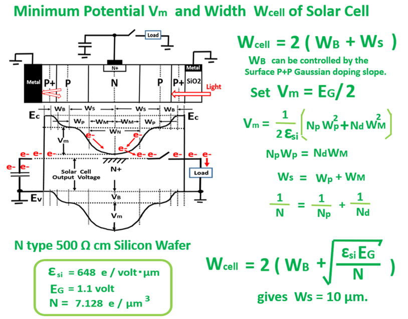
JPG050_P2020_Minimum_Potential_and_Width_of_Solar_Cell.jpg
JPG051_Pinne_Photodiode_Solar_Cell.jpg
JPG052_Pinned_Photodiode_Surface_Barrier_Potential.jpg
+++++++++++++++++++++++++++++++++++++++++++++++++++++++++++++
JPG053_Pinned_Photodiode_Surface_Barrier_Potential_1.jpg
JPG054_Pinned_Photodiode_Surface_Barrier_Potential_2.jpg
JPG055_Pinned_Photodiode_Surface_Barrier_Potential_3.jpg
JPG056_Proposal_of_Pinned_Photodiode_type_Solar_Cell.jpg
JPG057_Proposal_of_Pinned_Photodiode_type_Solar_Cell_01.jpg
JPG058_Proposal_of_Pinned_Photodiode_type_Solar_Cell_02.jpg
JPG059_Proposal_of_Pinned_Photodiode_type_Solar_Cell_03.jpg
JPG061_Proposal_of_Pinned_Photodiode_type_Solar_Cell_04.jpg
JPG062_Proposal_of_Pinned_Photodiode_type_Solar_Cell_05.jpg
JPG063_Proposal_of_Pinned_Photodiode_type_Solar_Cell_06.jpg
JPG064_Proposal_of_Pinned_Photodiode_type_Solar_Cell_07.jpg
JPG065_Proposal_of_Pinned_Photodiode_type_Solar_Cell_09.jpg
JPG066_Proposal_of_Pinned_Photodiode_type_Solar_Cell_10.jpg
JPG067_Proposal_of_Pinned_Photodiode_type_Solar_Cell_11.jpg
JPG068_PS3_Cell_Proceesor_Sony_Team_Award.jpg
JPG069_Self_Driving_Car_TV_interview_2013.jpg
JPG070_Simple_PN_junction_Solar_Cell.jpg
JPG071_Slide019A_Sony_Atsugi_Tech_2020_07_10.jpg
JPG072_Slide023A_Sony_Atsugi_Tech_2020_07_10.jpg
JPG073_Solar_Cell_with_High_Blue_Light_Sensitivity.jpg
JPG074_Sony_Atsugi_Tech_Lab_Note_in_Summer_1971_by_Yoshiaki_Daimon_Hagiwara.jpg
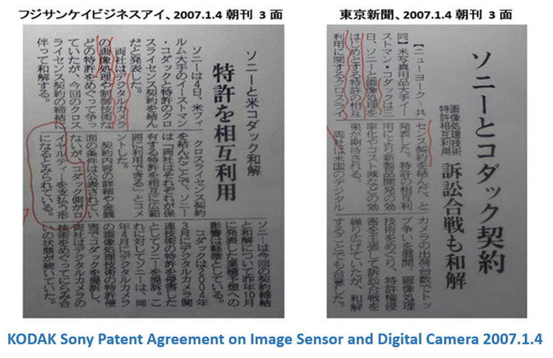
JPG075_Sony_Kodak_Patent_Agreement.jpg
JPG076_Three_types_of_in_pixel_Vertical_Overflow_Drain_VOD.jpg
+++++++++++++++++++++++++++++++++++++++++++++++++++++++++++++++++++++++++
PDF001_Buried_Photodiode_is_not_always_PPD_Hagiwara_Nov_2020.pdf
PDF002_Difference_of_Pinned_Photodiode_and_Buried_Photodiode_1.pdf
PDF003_E-mail_Communication_on_Sony_Loral_Patent_War_1996.pdf
PDF004_E-mail_communication_with_Albert_and_Yoshi.pdf
PDF004_E-mail_communication_with_Albert_san_2018_07_10A.pdf
PDF004_E-mail_communication_with_Albert_san_2018_07_10B.pdf
PDF005_Evidence_that_Hagiwara_is_the_inventor_of_Pinned_Photodiode_in_Japanese.pdf
PDF006_Hagiwara_invented_PPD_and_Sony_HAD_in_1975.pdf
PDF007_Image_Sensor_Story_07.pdf
PDF008_Image_Sensor_Story_14.pdf
PDF009_Origin_of_1975_Concept_of_Pinned_Photodiode_.pdf
PDF010_The_evidence_that_Hagiwara_is_the_inventor_of_Pinned_Photodiode_2020_10_02 .pdf
+++++++++++++++++++++++++++++++++++++++++++++++++++++++++++++
JP1975-127646.pdf
JP1975-127647.pdf
JP1975-134985.pdf
JP1975-134985_JPA 1977058414.pdf
JP1975-134985_Patent_Claim_in_English_Translation.pdf
JP1977-837_Hitachi_Koike.pdf
JP1977-126885.pdf
JP1977-126885_Original.pdf
JP1978-1971_Toshiba_Yamada_VOD_patent.pdf
JP1980-138026_NEC_Teranishi_Patent.pdf
+++++++++++++++++++++++++++++++++++++++++++++
P1976_128_bit_Comparator.pdf
P1978_Pinned_Photodiode_1978_Paper_by_Hagiwara.pdf
P1979_CCD79_in_Edinbourgh_1979.pdf
P1989_SONY_4MSRAM_1989.pdf
P1996_Pinned_Photodidoe_used_in_Sony_1980_FT_CCD_Image_Sensor.pdf
+++++++++++++++++++++++++++++++++++++++++++++++++++++++++++++
P2001_ESSCIRC2001.pdf
P2008_ESSCIRC2008Hagiwara.pdf
P2013_ISSCC2013PanelTalk.pdf
P2019_3DIC2019Paper_on_3D_Pinned_Photodiode.pdf
P2020_EDTM2020_PaperID_3C4_by_Hagiwara.pdf
P2020_Pinned_Photodiode_Solar_Cell_1.pdf
P2020_Pinned_Photodiode_Solar_Cell_2.pdf
+++++++++++++++++++++++++++++++++++++++++++++++++++++++++++++
*********************************************************************
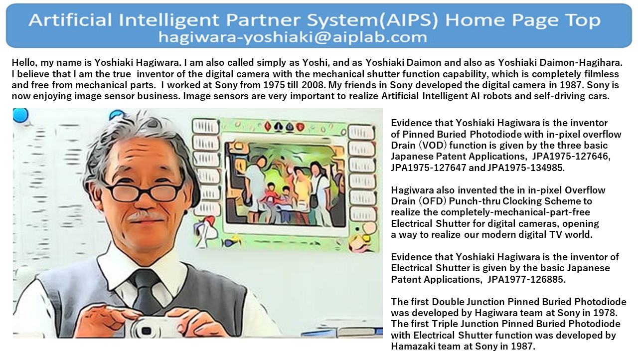
Please write me freely anything related to my activities: *********************************************************************
hagiwara-yoshiaki@aiplab.com for my activity at http://www.aiplab.com/
hagiwara@ssis.or.jp for my activity at http://www.ssis.or.jp/en/index.html
*********************************************************************