****************************************************
The most important Image Sensor Patents
in 1975, 1977 and 2014 by Yoshiaki Hagiwara
******************************************************
This is the original Hagiwara 1975 Japanese Patent Idea
Japanese Patent Application 1975-127646
http://www.aiplab.com/JP1975-127646.pdf
on the original N+NP+NP junction Buried Pinned Photodiode
******************************************************
Note that this is the N+NP+NP junction type Buried Photodiode.
This is also a Pinned Photodiode with the surface N+ region pinned,
with the thyrisor punch thru operation for the image charge transfer
and the MOS capacitor buffer memory for Global Shutter Operation.
******************************************************
This is the original Hagiwara 1975 Japanese Patent Idea
Japanese Patent Application 1975-127647
http://www.aiplab.com/JP1975-127647.pdf
on the original N+NP+N junction Buried Pinned Photodiode
******************************************************
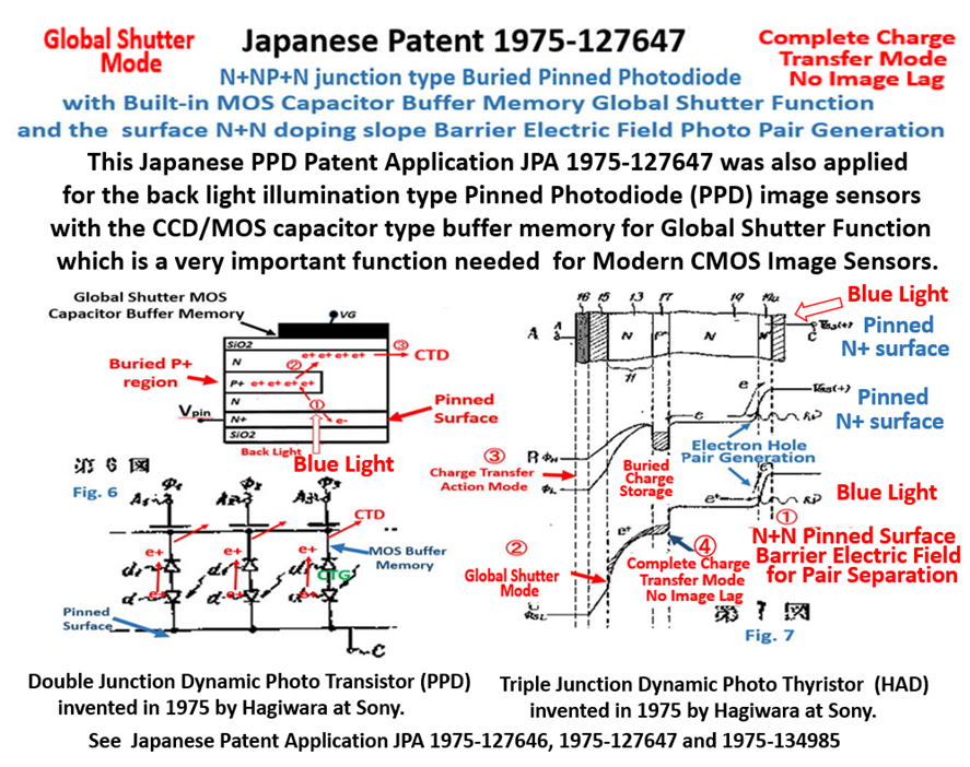
Note that this is the P+PN+P junction type Buried Photodiode.
This is also Pinned Photodiode with the pinned surface P+ region
with MOS Capacitor Global Shutter Memory for the image lag free
complete charge transfer operation with Back Light Illumination.
This is the original basic patent on Pinned Photodiode with
Global Shutter function needed for CMOS Image Sensors.
******************************************************
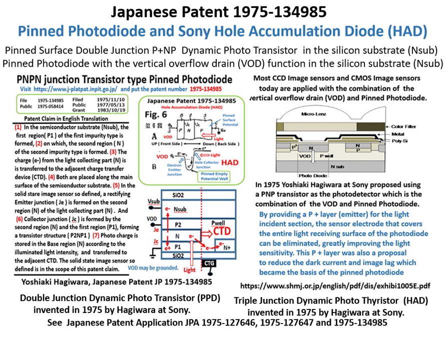
This is the original Hagiwara 1975 Japanese Patent Idea
Japanese Patent Application 1975-134985
http://www.aiplab.com/JP1975-134985.pdf
on the original P+NPNsub junction Buried Pinned Photodiode with
the vertical overflow drain (VOD) function needed to have the
electric shutter function for filmless and chanical free cameras.
*****************************************************
******************************************************
This is the original Hagiwara 1975 Japanese Patent Idea
Japanese Patent Application 1977-126885
http://www.aiplab.com/JP1977-126885.pdf
on the original Mechanical-Free Electric Function Photodiode.
*****************************************************
******************************************************
Note that the electrical shutter function can be possbile only
for the image lag free bult-in VOD type Pinned Photodiode.
*****************************************************
******************************************************
This is the most recent Hagiwara 2014 Japanese Patent Idea
Japanese Patent Application 2014-135479
http://www.aiplab.com/JP2014-135479.pdf
on 1/N sampling hold fast frequency Transfroamtion Method.
*****************************************************
To get the Original Japanese Patent Claims,
please visit Japanese Patent Official Web Site.
https://www.j-platpat.inpit.go.jp.
The followings are the evidence that Hagiwara invented Pinned Photodiode.
(1) Japapese Patent Application JPA 1975-127646
http://www.aiplab.com/JP1975-127646.pdf
(2) Japapese Patent Application JPA 11975-127647
http://www.aiplab.com/JP1975-127647.pdf
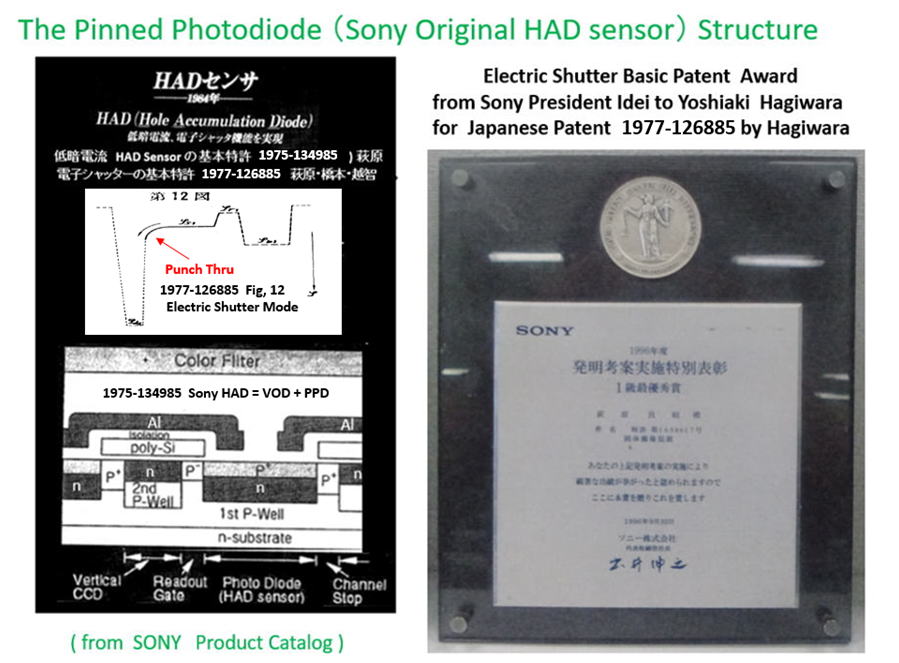
(3) Japapese Patent Application JPA 11975-134985
http://www.aiplab.com/JP1975-134985.pdf
(4) Japapese Patent Application JPA 11977-126885
http://www.aiplab.com/JP1977-126885.pdf
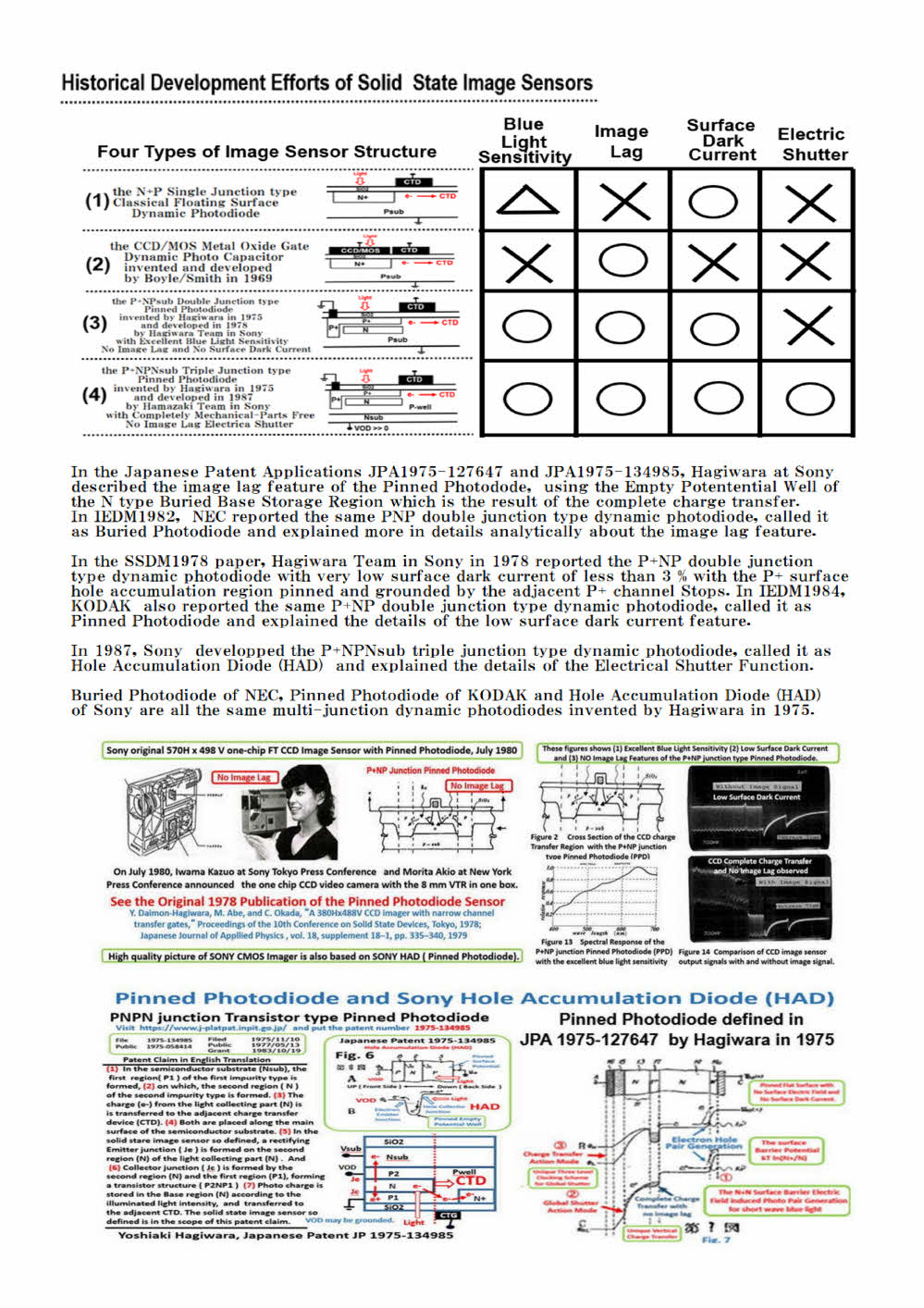
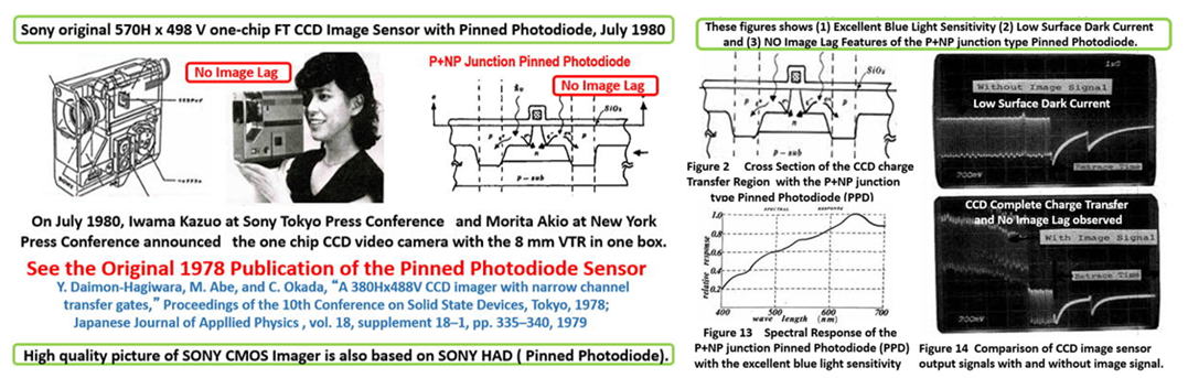
(5) SSDM_1978_Conference Paper on P+NP Pinned Photodiode
"A 380H X 488V CCD Imager with Narrow Channel Transfer Gates"
SSDM1978 Conference Paper September 1978 and Japanese Journal
of Applied Physics, Volume 18 Sup 18-1, pp.335-340 November 1979
http://www.aiplab.com/P1978_Pinned_Photodiode_1978_Paper_by_Hagiwara.pdf
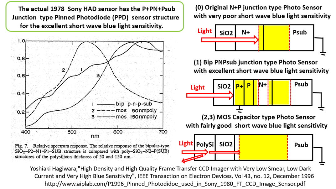
(6) IEEE_EDS_Journal_1966Paper
"High Density and High Quality Frame Transfer CCD Imager with
Very Low Smear, Low Dark Current and Very High Blue Sensitivity",
IEEE Transaction on Electron Devices, Vol 43, no. 12, December 1996
http://www.aiplab.com/P1996_Pinned_Photodidoe_used_in_Sony_1980_FT_CCD_Image_Sensor.pdf
(7) IEEE_3DIC2019_Conference_Paper
"Multichip CMOS Image Sensor Structure for Flash Image Acquisition"
IEEE International 3D Systems Integration Conference 2019 (3DIC2019)
Digest of Technical Papers, Sendai, Japan, Paper4017, October 2019
http://www.aiplab.com/P2019_3DIC2019Paper_on_3D_Pinned_Photodiode.pdf
(8) IEEE_EDS_EDTM2020_Paper
"Simulation and Device Characterization of the P+PN+P Junction Type
Pinned Photodiode and Schottky Barrier Photodiode"
IEEE Electron Device and Manufacturing Technology Conference (EDTM2020),
Digest of Technical Papers, Penang Malaysia, Paper ID 3D6, March 2020
http://www.aiplab.com/P2020_EDTM2020_PaperID_3C4_by_Hagiwara.pdf
Yoshiaki Hagiwara wrote a book on
"the World of Artificial Intelligent Digital Circuits",
which is important and needed to built
the intelligent image sensor systems.
ISBM978-4-88359-339-2
Hard Cover, 460 page,
\ 9000 Japanese Yen + tax
If you are interestied in the book, Please visit
https://www.seizansha.co.jp/ISBN/ISBN978-4-88359-339-2.html
https://www.seizasha.co.jp/
*************************************************************
The following four Japanese Patent Applications explained that
Hagiwara invented Pinned Photodiode with VOD function in 1975.
index001_Image_Sensor_1975_1977_and_2014_Patents.html
*************************************************************
index002_Facts_on_Invention_of_Pinned_Photodiode.html
index003_Hagiwara_Publication_List.html
index004_My_Wonderful_Memory_Pictures.html
index005_Image_Sensor_Story_by_Hagiwara.html
*************************************************************
********************************************************
hagiwara-yoshiaki@aiplab.com http://www.aiplab.com/
hagiwara@ssis.or.jp http://www.ssis.or.jp/en/index.html
********************************************************
******************************
Return to Top Page
http://www.aiplab.com/
*********************************