Slide_Top
+++++++++++++++++++++++++++++++++++++++++++++++++++++++++++++++++++++++++++++++
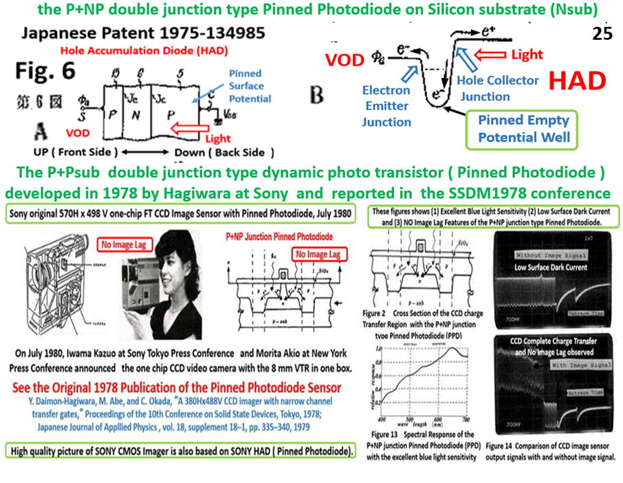
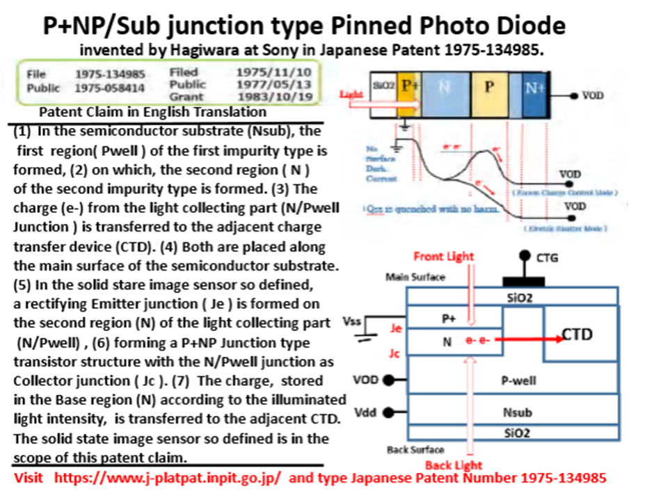
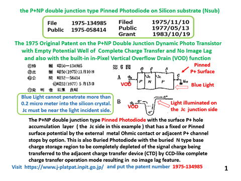
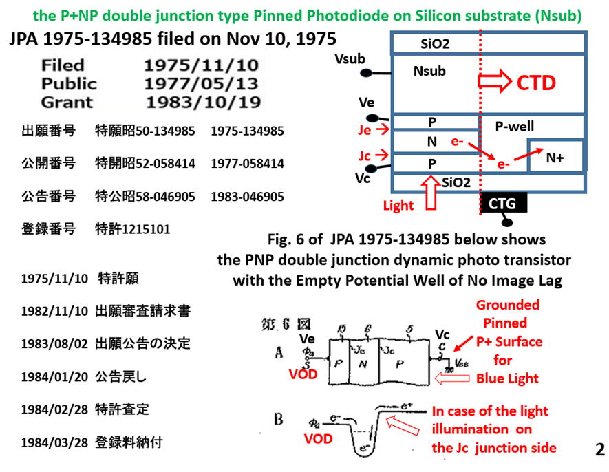
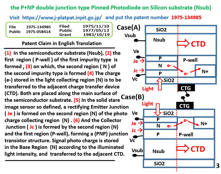
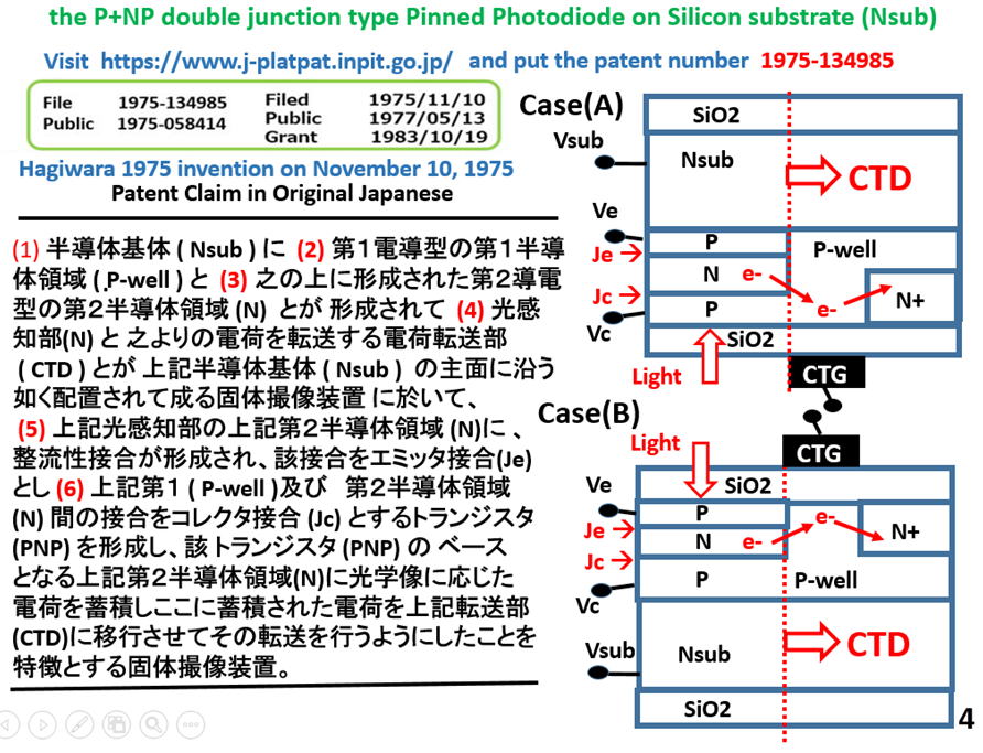
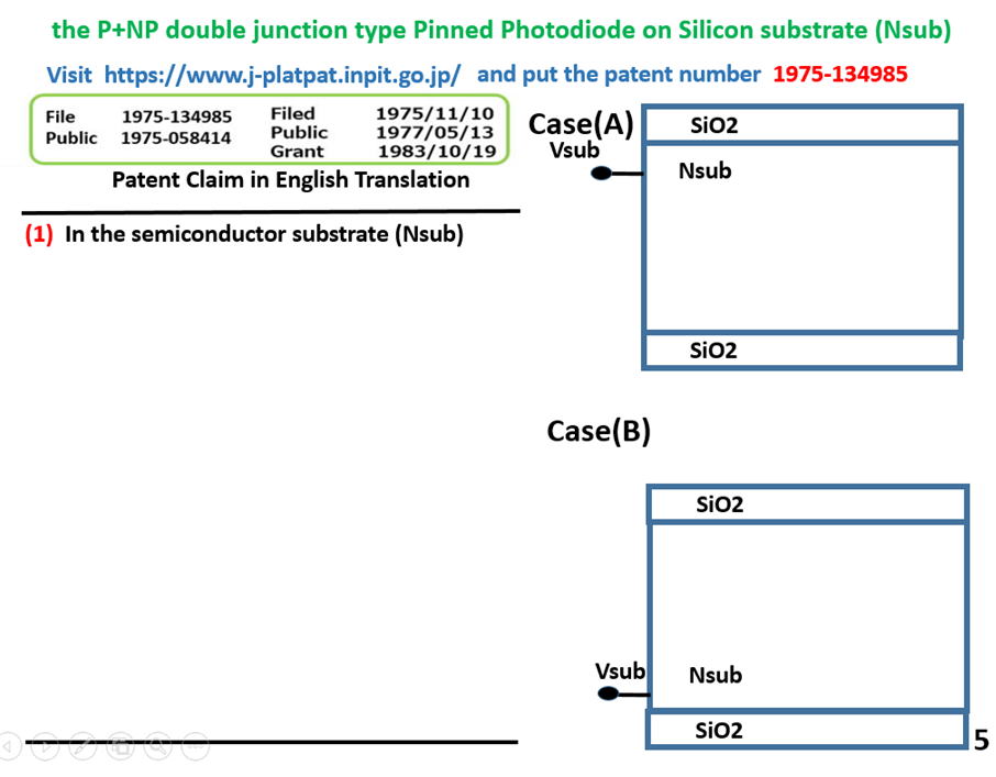
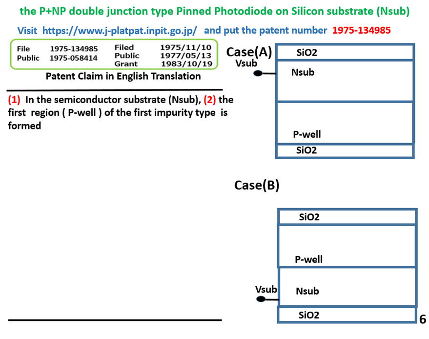
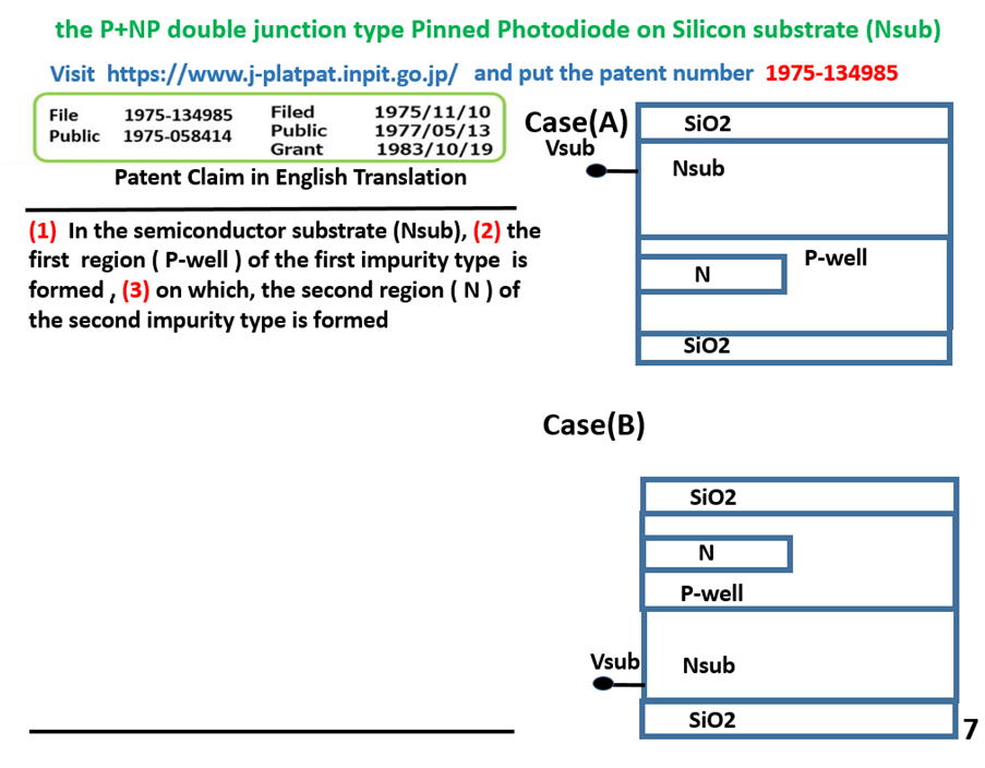
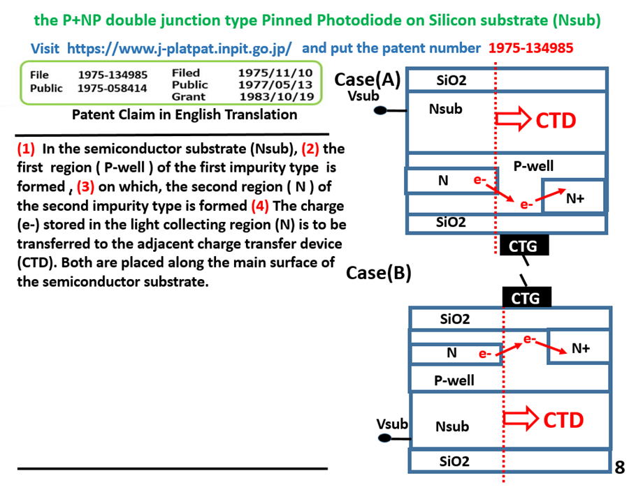
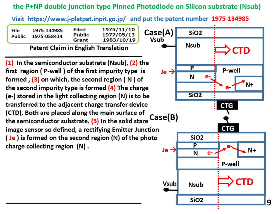
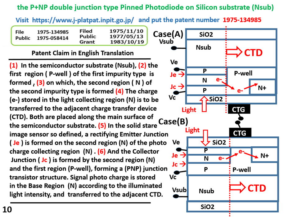
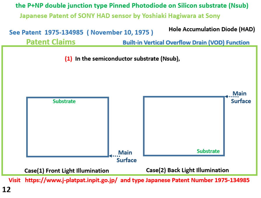
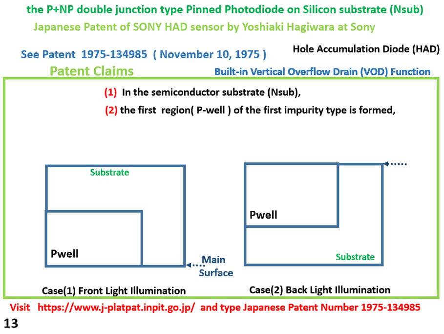
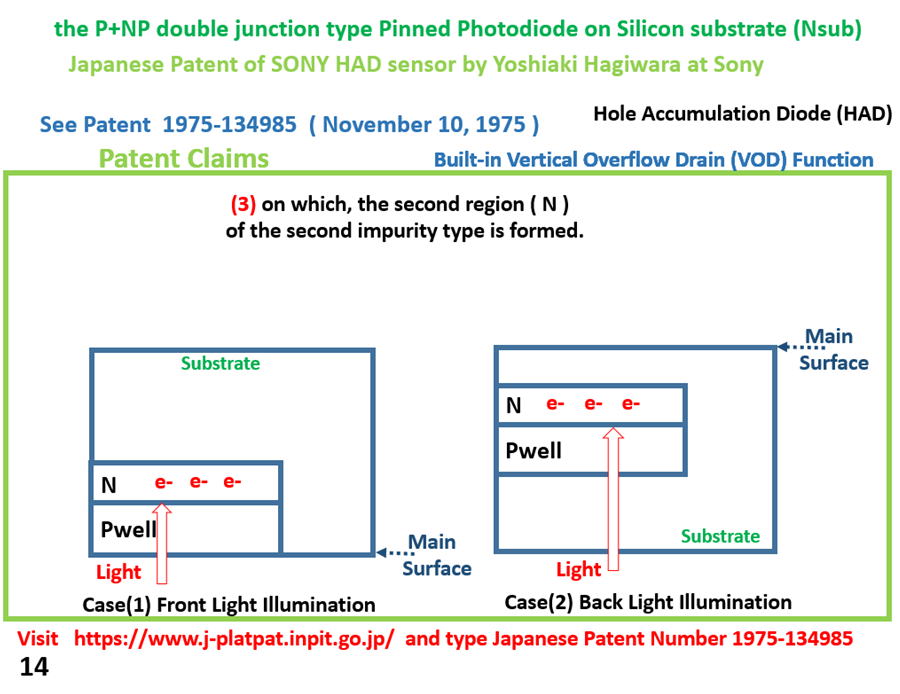
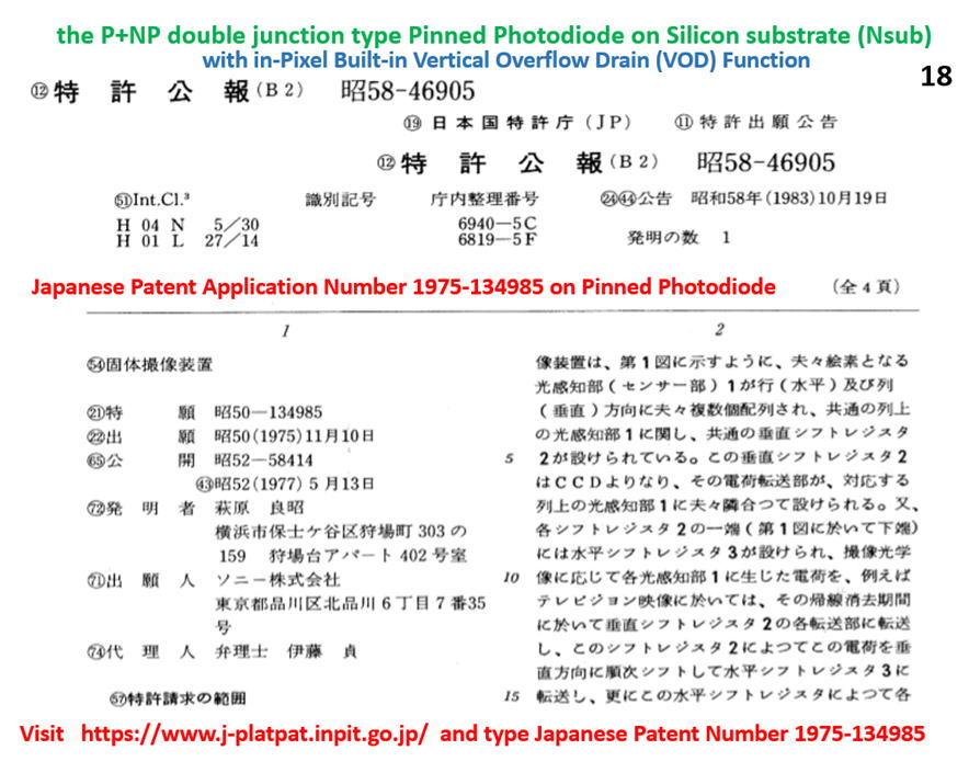
This is an English translation of the Japanese Patent Claims
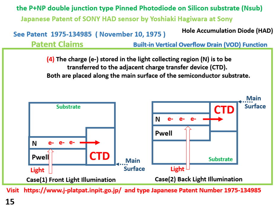
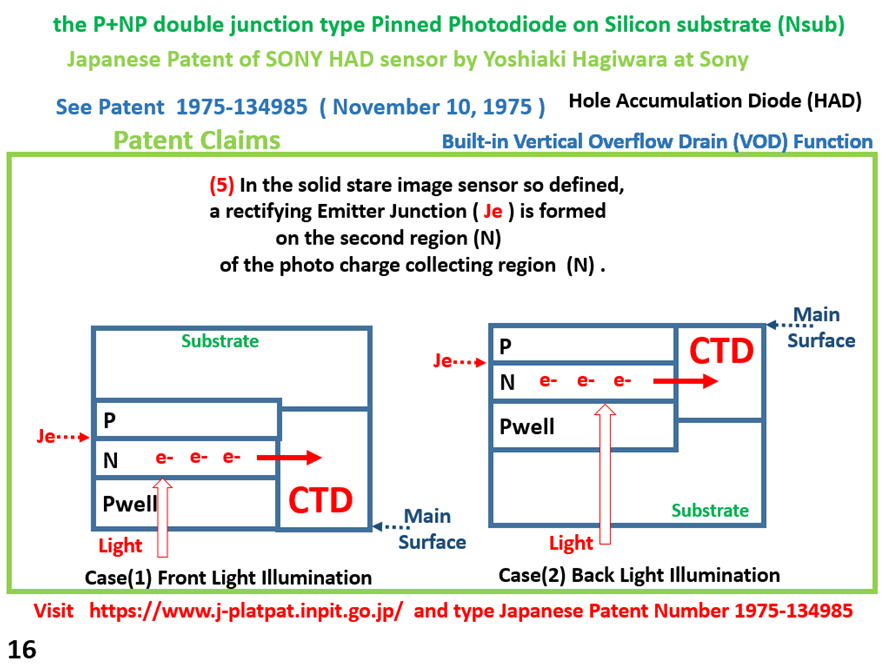
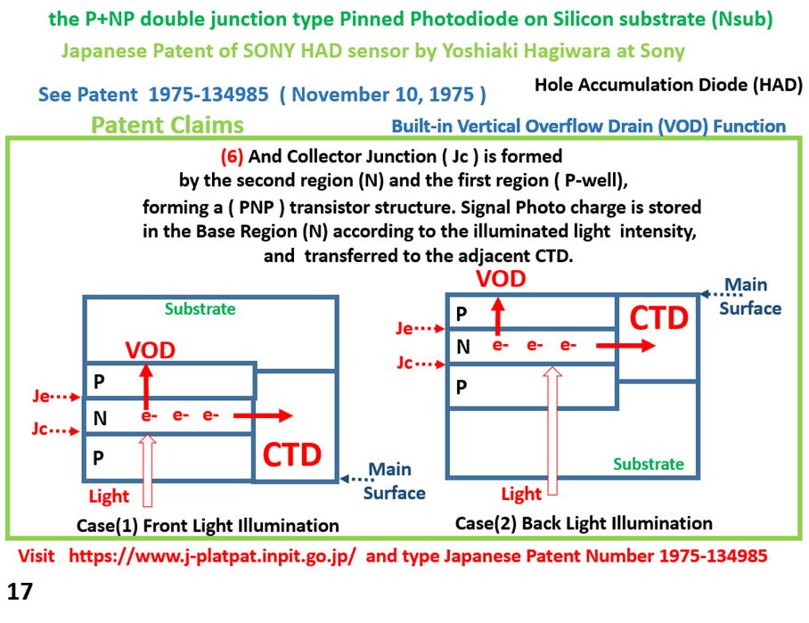
applied in 1975 by Hagiwara at Sony on the PNP double junction type
dynamic photo transistor on the substrate with the P+ Pinned Surface
Hole Accumulation Layer with the Vertical Overflow Drain (VOD) function.
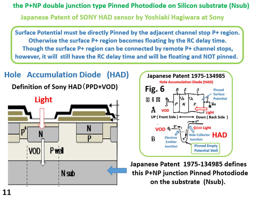
In November 1975 Hagiwara proposed the double junction dynamic photo transistor
which was later called as Pinned Photodiode by Kodak in 1984 and later
also as
Sony original Hole Accumulation Diode (HAD).
The main purpose of Hagiwara 1975 invention was the advantagious and exccellent
features of the short wave blue light sensitivity and the in-pixel built-in vertical
overflow drain (VOD) function with no image lag feature.
In the figure 6 of this Japanese Patent Application JPA 1975-134985, Hagiwara
drew
fo the first time in the world the empty potential well, which shows the complete charge
transfer capability, the evidence of no image lag feature for fast action
pictures.
++++++++++++++++++++++++++++++++++++++++++++++++++++++++++++++++++++++++++++++++
Slide001
Slide002
Slide003
Slide004
Slide005
Slide006
Slide007
Slide008
Slide009
Slide010
Slide011
Slide012
Slide013
Slide014
Slide015
Slide016
Slide017
Slide018
Slide019
Slide020
Slide021
Slide022
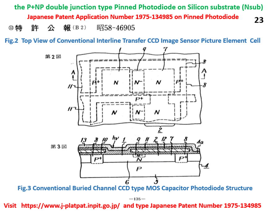
Slide023
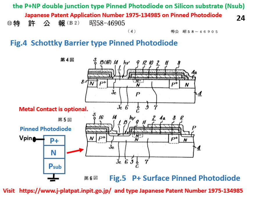
Slide024
Slide025