++++++++++++++++++++++++++++++++++++++++++++++++++++++++++++++
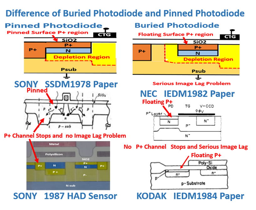
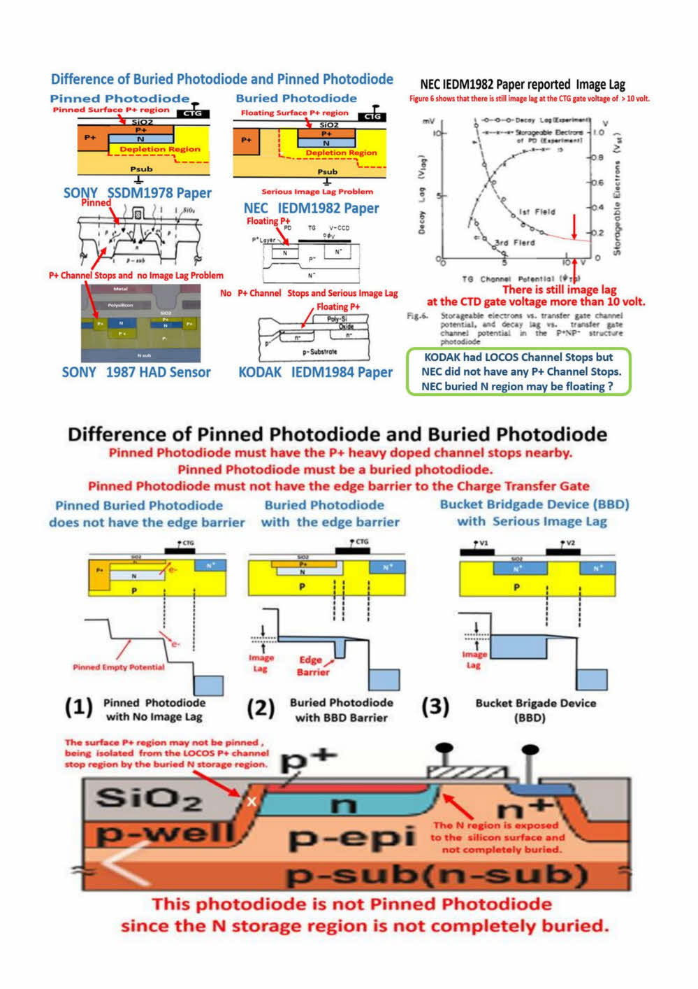
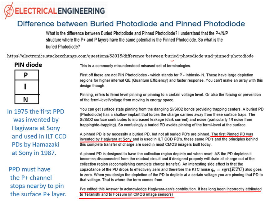
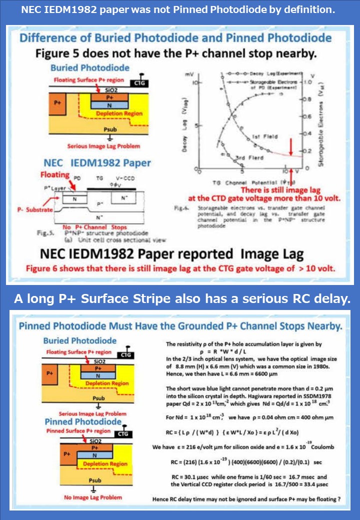
The problem is that very few people understand the difference
between Pinned Photodiode and Buried Photodiode.
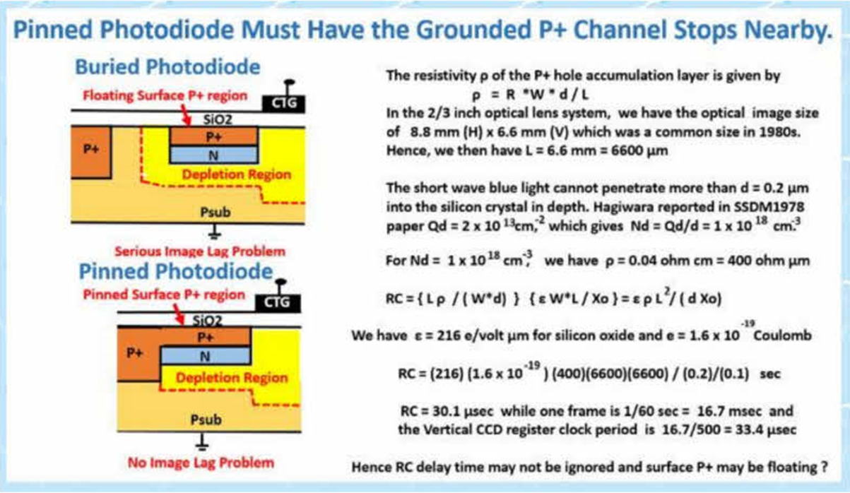
The P+ channel stops must be very close to each picture element area.
Otherwise there is a serious RC delay time, and the surface P+ region
becomes unstable and fluctuated by the clock couplings and results
in the undesired incomplete charge transfer and the serious image lag.
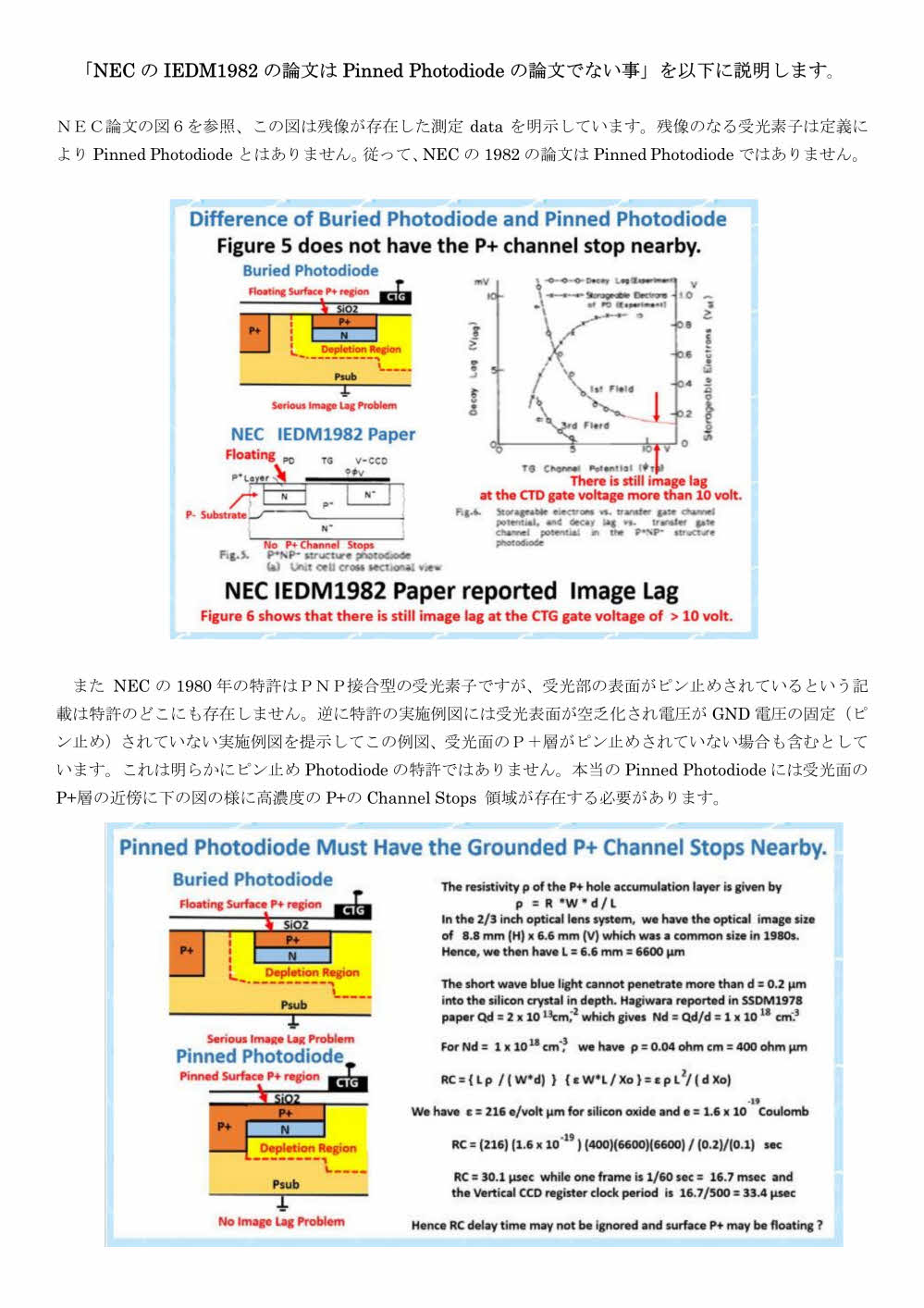
In the 1984 IEDM paper KODAK reported the use of LOCOS technoloy
and evidently there is the P+ channel stops in the LOCOS region.
Yes, KODAK 1984 Photodiode is evidently Pinned Photodiode.
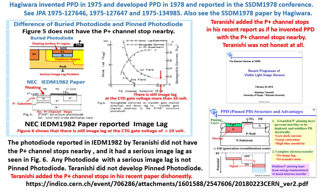
But the NEC IEDM1982 photodiode is NOT clearly a PPD.
Teranishi added the P+ channel stops in his recent publications dishonestly. Why ???
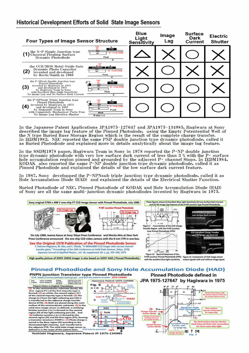
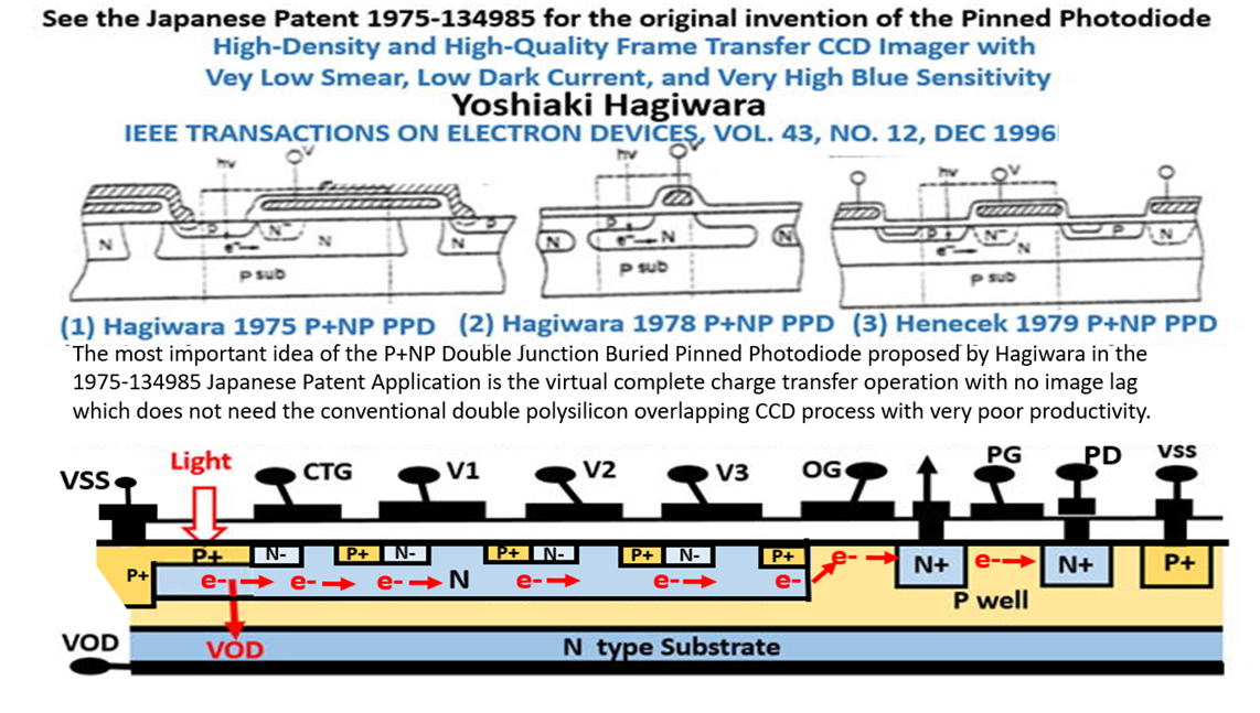
In either way, Hagiwara invented the PPD in 1975 and drew the empty potential wells
of the complete charge transfer operation which enables the virtual charge transfer.
If any portion of the N type charge collecting region is exposed to the silicon surface,
it is by definition NOT Buried Photodiode, hence it is NOT Pinned Photodiode.
++++++++++++++++++++++++++++++++++++++++++++++++++++++++++++++++++++++++++++++++++++++++++++++++++++++++++++++++++++++++++++++++++++++
The problem is that very few people understand the difference
between Pinned Photodiode and Buried Photodiode.
Difference_of_Pinned_Photodiode_and_Buried_Photodiode.jpg
The P+ channel stops must be very close to each picture element area.
Otherwise there is a serious RC delay time, and the surface P+ region
becomes unstable and fluctuated by the clock couplings and results
in the undesired incomplete charge transfer and the serious image lag.
RC_Delay_of_Flaoting_Buried_Photodiode.jpg
KODAK used LOCOS and evidently there is P+ channel stops in the LOCOS region.
Yes, KODAK 1984 Photodiode is evidently Pinned Photodiode.
Difference_of_Buried_Photodiode_and_Pinned_Photodiode_1.jpg
But NEC IEDM1982 photodiode is NOT clearly PPD.
Teranishi added the P+ channel stops in his recent publications dishonestly. Why ???
Hagiwara_is_the_inventor_of_PPD_not_Teranishi.jpg

Hagiwara_invented_PPD_and_Virtual_Charge_Transfer.jpg
If any portion of the N type charge collecting region is exposed to the silicon surface,
it is by definition NOT Buried Photodiode, hence NOT Pinned Photodiode.
Difference_of_Pinned_Photodiode_and_Buried_Photodiode_1.jpg
+++++++++++++++++++High Light ++++++++++++++++++
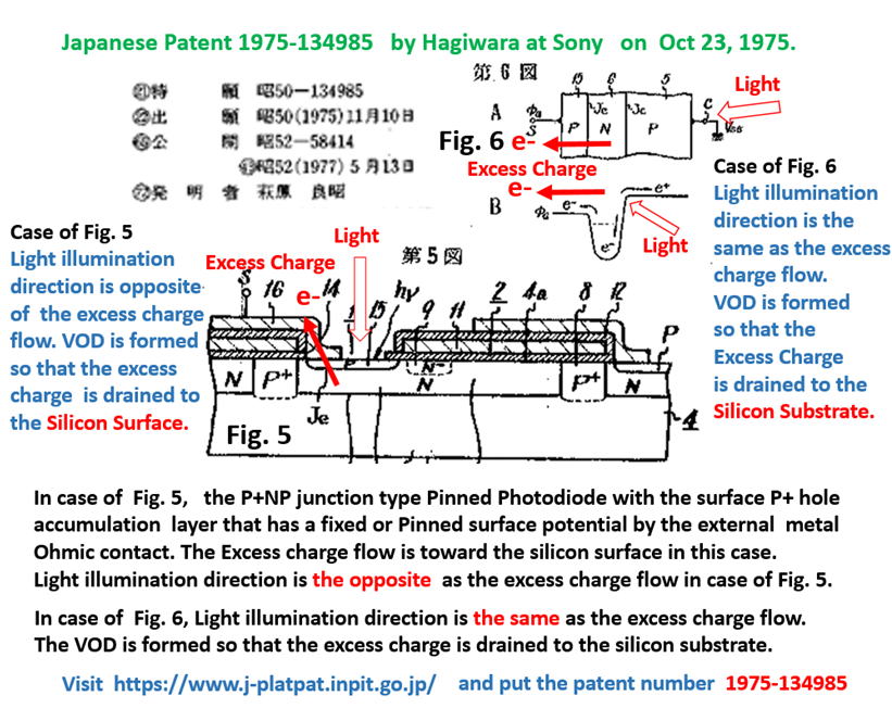
Hagiwara 1975 Pinned Photodiode Patent : JPA_1975_134985/index.html
IEEE_EDTM2020_Paper_on_Pinned_Photodiode_by_Yoshiaki_Hagiwara.html
P2019_3DIC2019Paper_on_3D_Pinned_Photodiode.pdf
P2020_EDTM2020_PaperID_3C4_by_Hagiwara.pdf
P2020_Pinned_Photodiode_Solar_Cell_1.pdf
P2020_Pinned_Photodiode_Solar_Cell_2.pdf
++++++++++++++++++++++++++++++++++++++++++++++
index001_Image_Sensor_1975_1977_and_2014_Patents.html
index002_Facts_on_Invention_of_Pinned_Photodiode.html
index003_Hagiwara_Publication_List.html
index004_My_Wonderful_Memory_Pictures.html
index005_Image_Sensor_Story_by_Hagiwara.html
index006_Invention_of_Pinned_Photodiode_in_1975.html
++++++++++++++++++++++++++++++++++++++++++++++
JPG021_All_Misunderstandings_on_PPD_inventions_
should_be_clearified_by_Hagiwara_1975_PPD_Patent_Applications.
http://www.aiplab.com/Image_Sensor_Story_14.jpg
JPG022_NEC(Teranishi)_did_not_invented_PPD_in_1979_
and_the_IEDM1982_Teranishi_Photodiode_was_NOT_PPD
http://www.aiplab.com/image3B_Hagiwara_at_Sony_invented_Pinned_Photodiode_in_1975.jpg
JPG023_Difference_of_Buried_Photodiode_and_Pinned_Photodiode_must_be_understood_clearly.
http://www.aiplab.com/Difference_of_Pinned_Photodiode_and_Buried_Photodiode_1.jpg
JPG024_Difference_of_Buried_Photodiode_and_Pinned_Photodiode_must_be_understood_clearly.
http://www.aiplab.com/Difference_of_Buried_Photodiode_and_Pinned_Photodiode_1.jpg
JPG025_Pinned_Photodiode_must_have_Adjacent_Channel_Stops_nearby_
........in order to_pin_the_surface_ P+_hole_accumulation_layer....
http://www.aiplab.com/Hagiwara_invented_PPD_and_Virtual_Charge_Transfer.jpg
![]()
JPG025_Hagiwara_invented_in_1975_the_P+NPsub double_junction_dynamic_photo_transistor_
http://www.aiplab.com/Difference_of_Static_and_Dynamic_Photo_Transistor.jpg
![]()
JPG026_Hagiwara_invented_the_Virtual_Phase_Charge_Transfer_in_1975
http://www.aiplab.com/Hagiwara_invented_PPD_and_Virtual_Charge_Transfer_in_1975_S01.jpg
![]()
JPG027_Hagiwara_invented_the_Virtual_Phase_Charge_Transfer_in_1975
http://www.aiplab.com/Hagiwara_invented_PPD_and_Virtual_Charge_Transfer_in_1975_S02.jpg
![]()
JPG028_Hagiwara_invented_the_Virtual_Phase_Charge_Transfer_in_1975
http://www.aiplab.com/Hagiwara_invented_PPD_and_Virtual_Charge_Transfer_in_1975_S03.jpg
![]()
JPG029_Hagiwara_invented_the_Virtual_Phase_Charge_Transfer_in_1975
http://www.aiplab.com/Hagiwara_invented_PPD_and_Virtual_Charge_Transfer_in_1975_S04.jpg
![]()
JPG030_Hagiwara_invented_the_Virtual_Phase_Charge_Transfer_in_1975
http://www.aiplab.com/Hagiwara_invented_PPD_and_Virtual_Charge_Transfer_in_1975_S05.jpg
![]()
JPG031_Hagiwara_invented_the_Virtual_Phase_Charge_Transfer_in_1975
http://www.aiplab.com/Hagiwara_invented_PPD_and_Virtual_Charge_Transfer_in_1975_S06.jpg
![]()
JPG032_Hagiwara_invented_the_Virtual_Phase_Charge_Transfer_in_1975
http://www.aiplab.com/Hagiwara_invented_PPD_and_Virtual_Charge_Transfer_in_1975_S07.jpg
![]()
JPG033_Hagiwara_invented_the_Virtual_Phase_Charge_Transfer_in_1975
http://www.aiplab.com/Hagiwara_invented_PPD_and_Virtual_Charge_Transfer_in_1975_S08.jpg
![]()
JPG034_Hagiwara_invented_the_Virtual_Phase_Charge_Transfer_in_1975
http://www.aiplab.com/P1996_no_image_lag_pinned_photo-diode_invented_in_1975_by_Hagiwara.jpg
JPG035_Hagiwara_invented_in_1975_
the_double_junction_dynamic_photo_transistor_and_
the_triple_junction_dynamic_photo_thyristor
http://www.aiplab.com/JP1975-134985_Patent_Claims_in_English_Translation.jpg
![]()
JPG036_Hagiwara_invented_in_1975_
the_double_junction_dynamic_photo_transistor_
with_no_image_lag_feature_and_VOD_function
http://www.aiplab.com/Two_type_of_VOD_in_JP1975-134985.jpg
JPG037_Most_important_Contribution_of_
Hagiwsara_1975_PPD_invention_
was_the_short_wave_blue_light_Sensitivity
http://www.aiplab.com/What_is_True_Pinned_Photodiode.jpg
JPG038_Most_important_Contribution_of_Hagiwsara_1975_PPD_invention_
was_the_short_wave_blue_light_Sensitivity
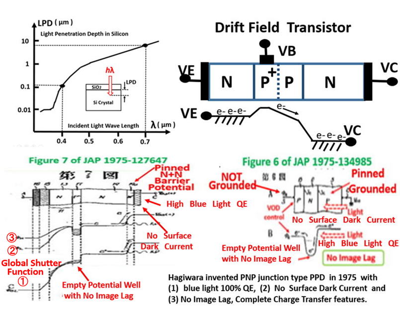
http://www.aiplab.com/Pinned_Photodiode_Drift_Field_Trasistor.jpg
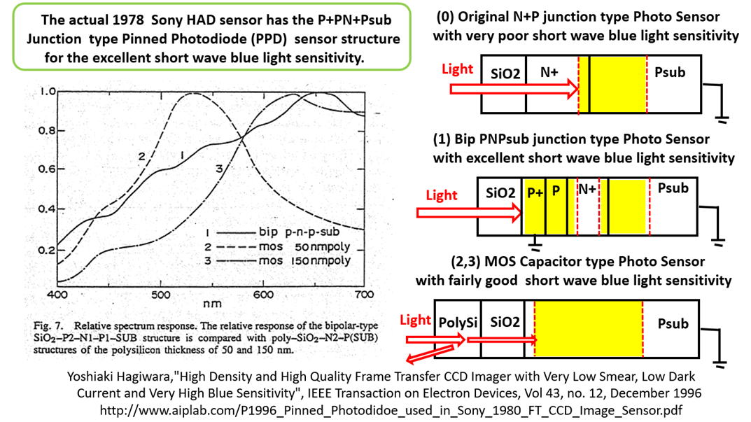
JPG039_Most_important_Contribution_of_Hagiwsara_1975_PPD_invention_
was_the_short_wave_blue_light_Sensitivity
http://www.aiplab.com/Pinned_Photodiode_Reported_in_Hagiwara_SSDM1978_Paper.jpg

+++++++++++++++++++++++++++++++++++++++++++++++++++++++++++++++++++++++++
l
*********************************************************************
Please write me freely anything related to my activities: *********************************************************************
hagiwara-yoshiaki@aiplab.com for my activity at http://www.aiplab.com/
hagiwara@ssis.or.jp for my activity at http://www.ssis.or.jp/en/index.html
*********************************************************************