++++++++++++++++++++++++++++++++++++++++++++++++++++++++++++++++++++++++++


Image Sensor Story by Yoshiaki Hagiwara

++++++++++++++++++++++++++++++++++++++++++++++++++++++++++++++++++++++++++

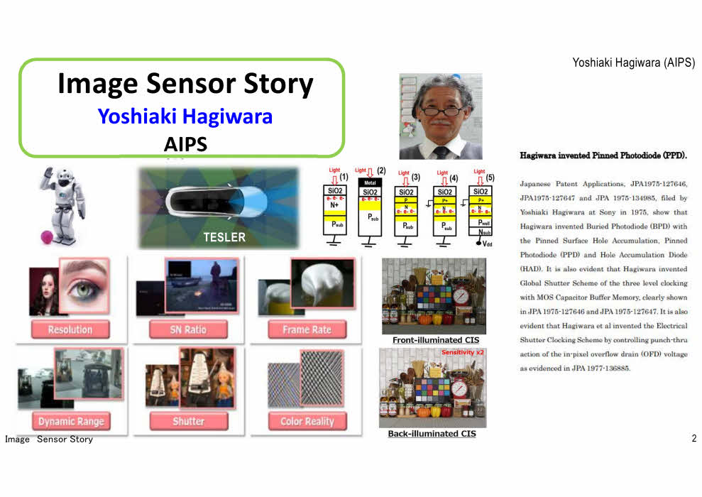
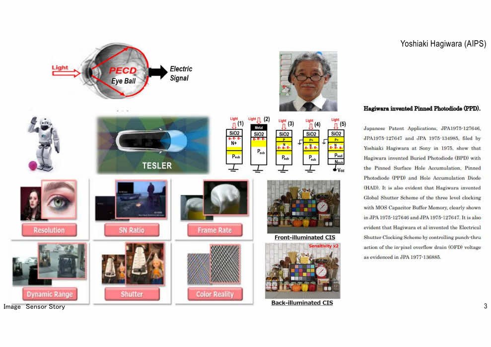
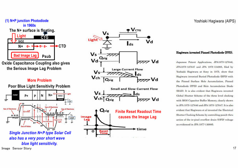
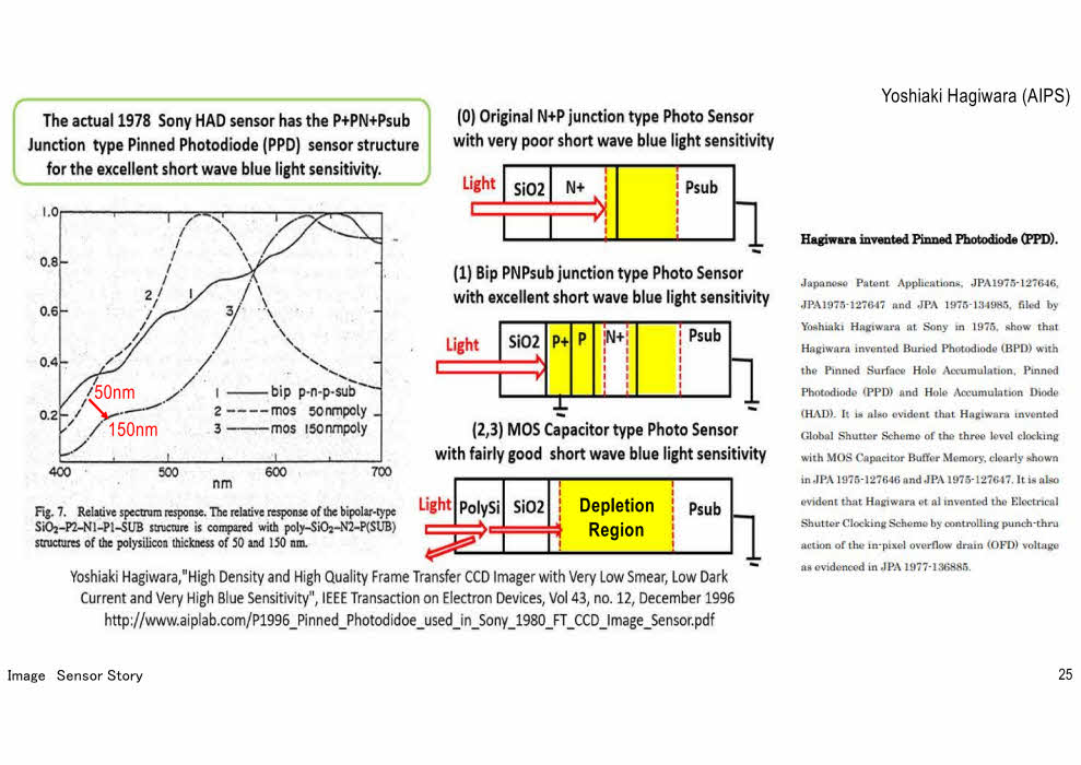
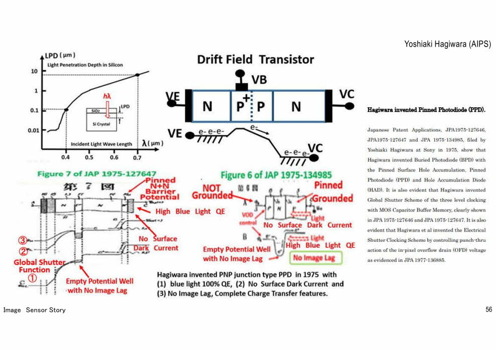
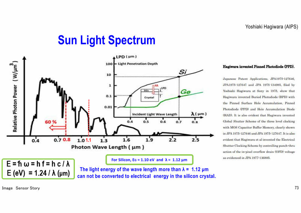
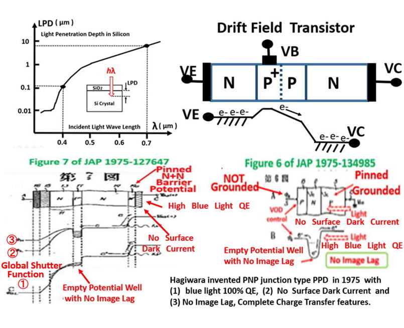
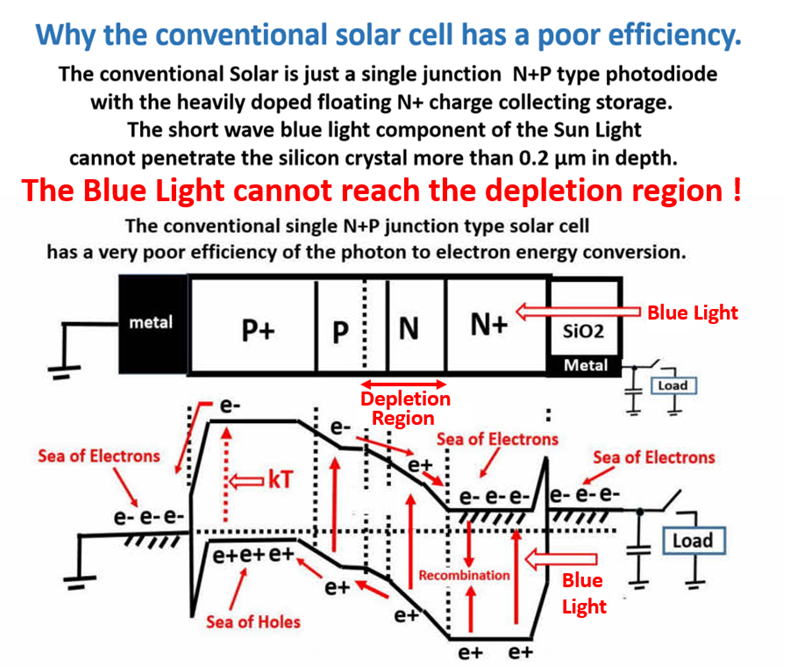
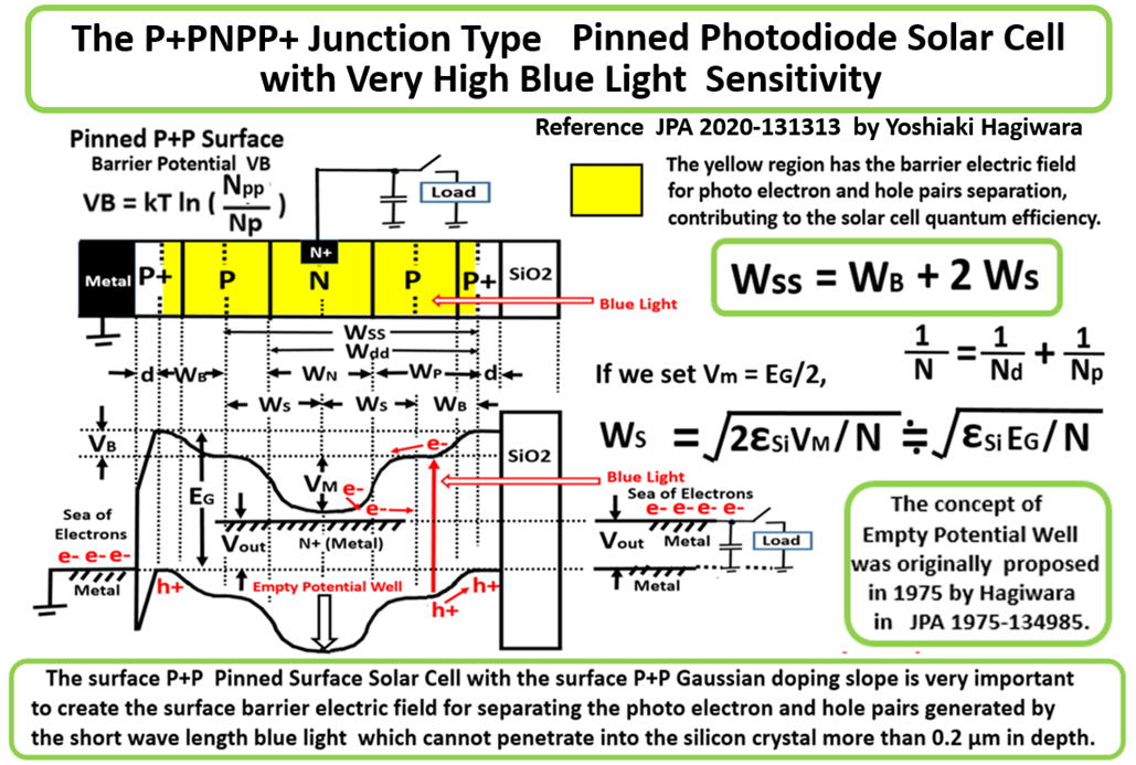
The most important feature of Image Sensor
is the short wave blue light sensitivity.

The short wave blue light cannot penetrate
more than 0.2 micro meter in depth of silicon crystal.

Usually the photo electron and hole pairs are
generated in the PN junction depletion region
which is deep inside the silicon crystal
of more than a few micro meters in depth.

Hence, the short wave blue light cannot reach
the PN junction depletion region.

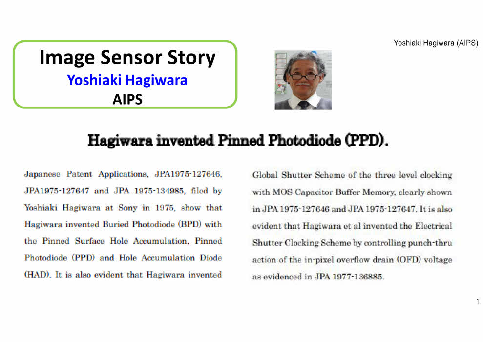
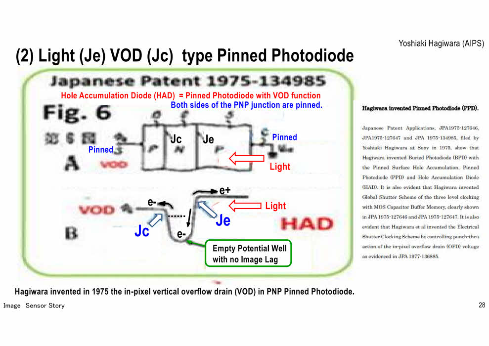
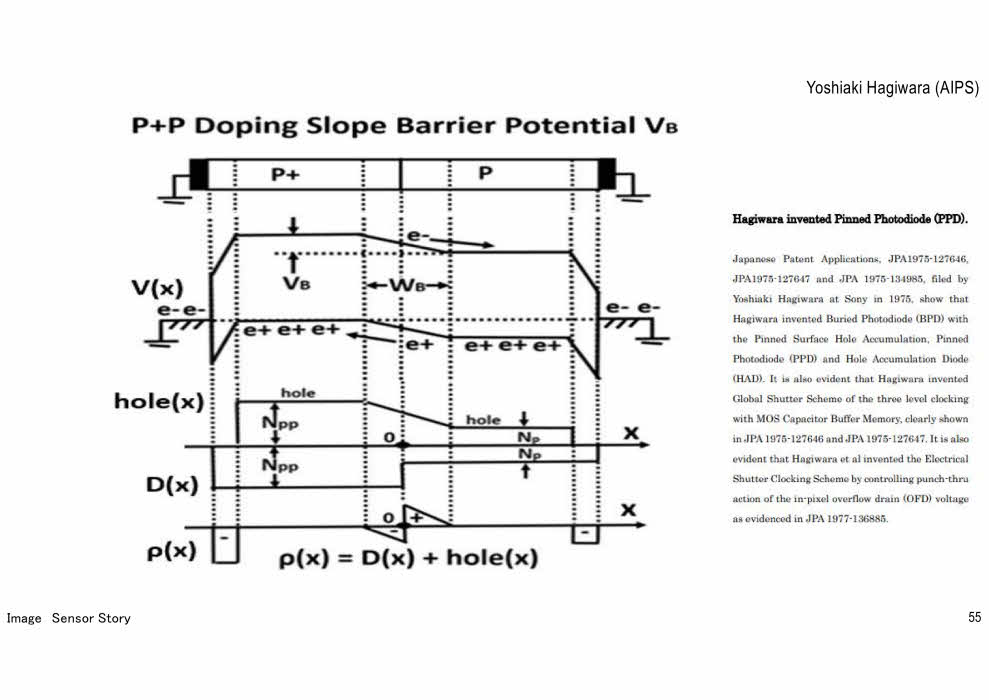
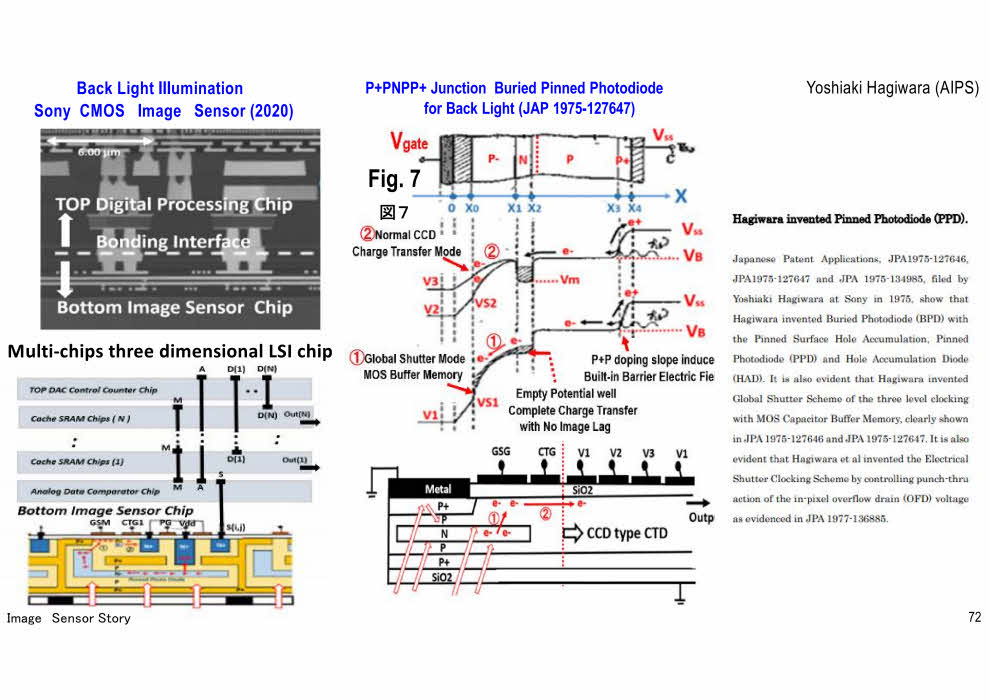
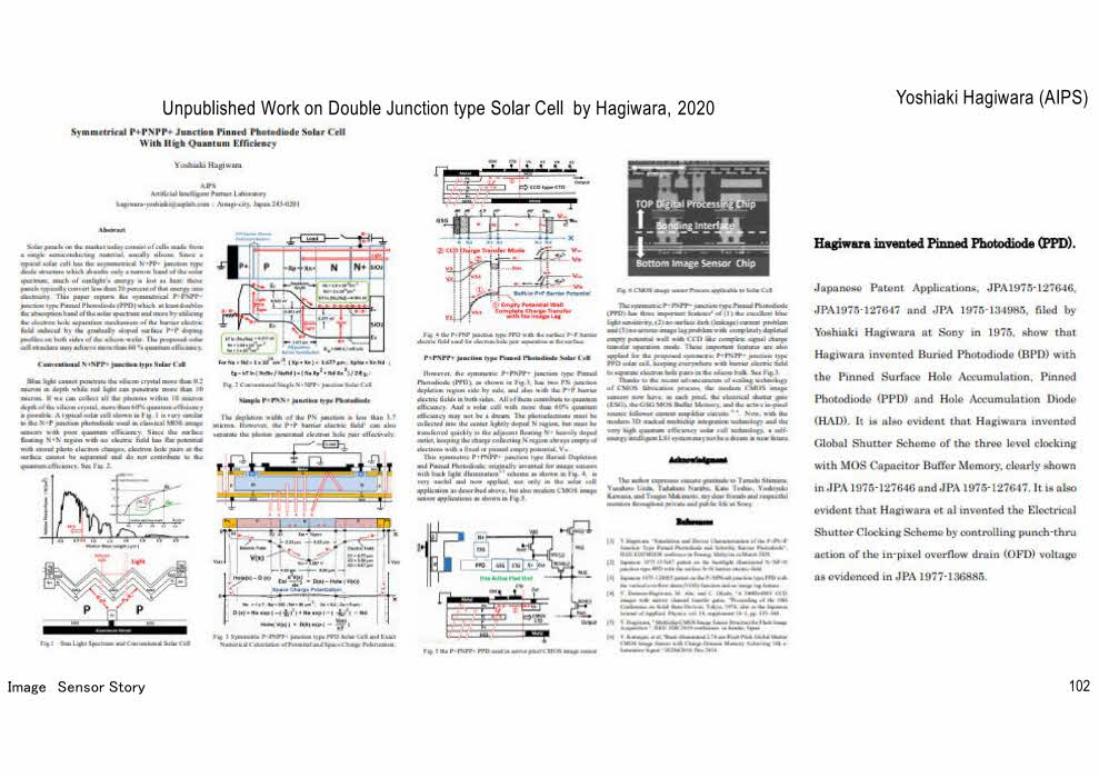
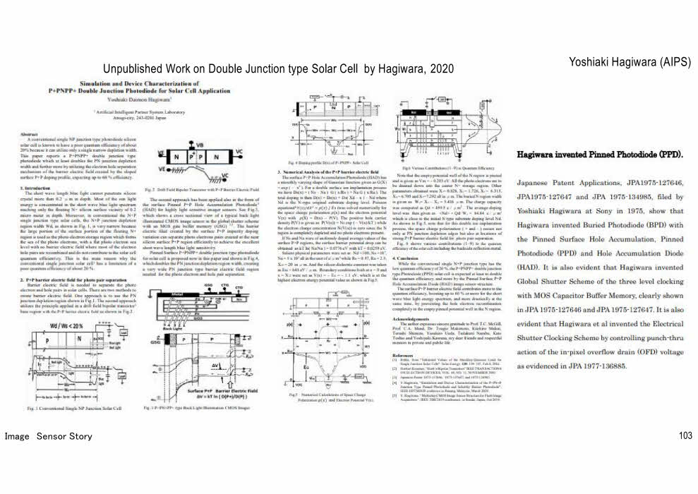
Yoshiaki Hagiwara in 1975 proposed
in Japanese Patent Applications
JPA 1975-127646 and JPA 1975-127647
that
the surface barrier field induced by
the surface Gaussian impurity atom doping slope
can be used to separate
the photo electron and hole pairs
generated at the silicon surface
of less than 0.2 micro meter in depth.

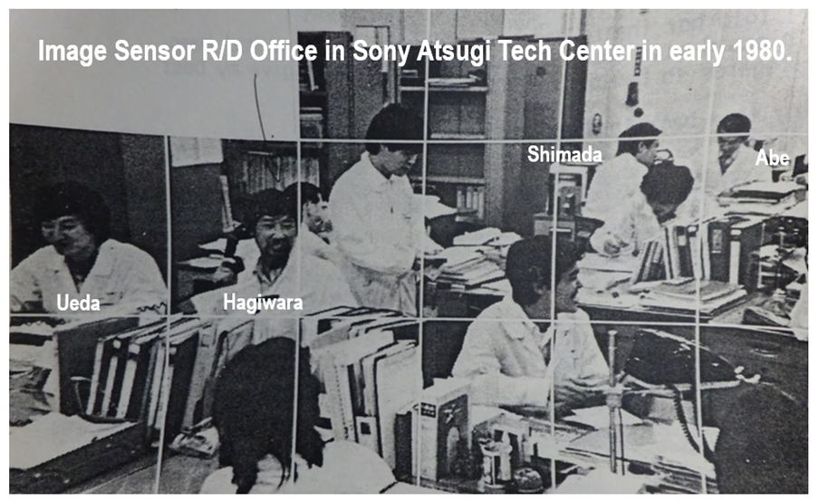
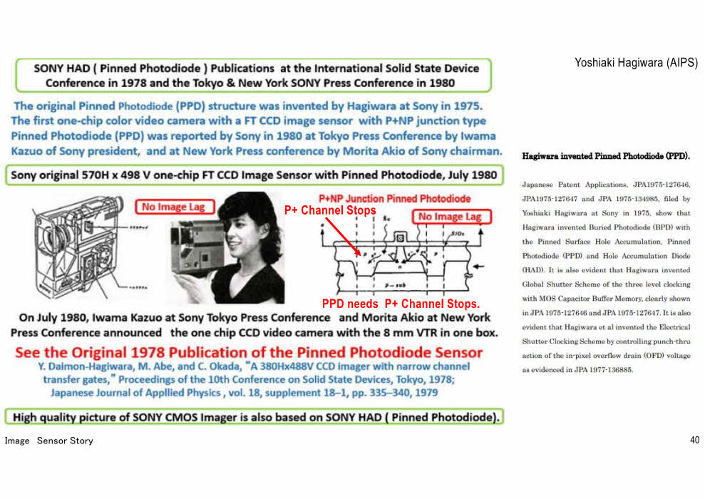
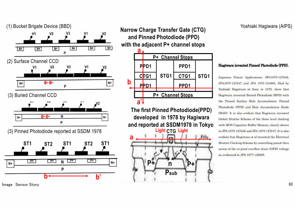
Yoshiaki Hagiwara in 1978 reported in SSDM1978 paper
the excellent blue light sensitivity
of P+NP double junction type Pinned Photodiode.

++++++++++++++++++++++++++++++++++++++++++++++++++++++++++++++++++++++++++


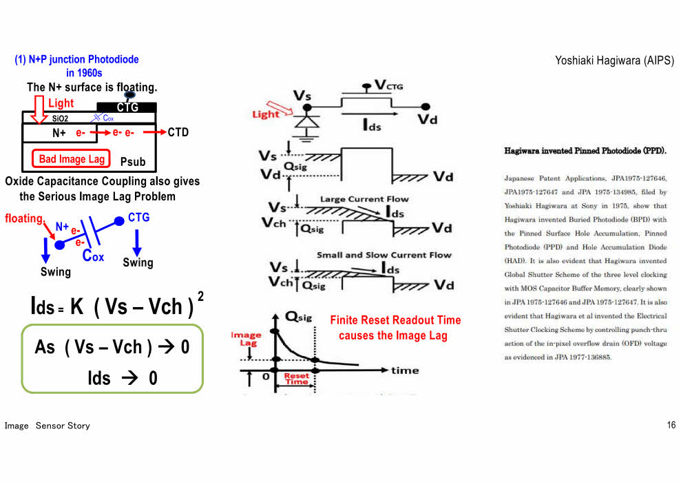
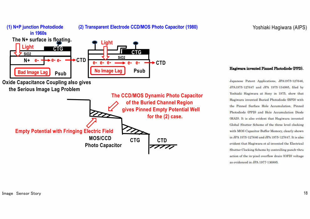
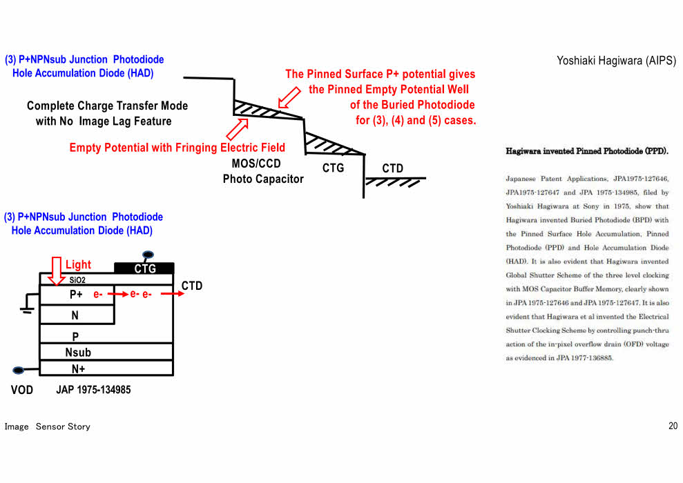
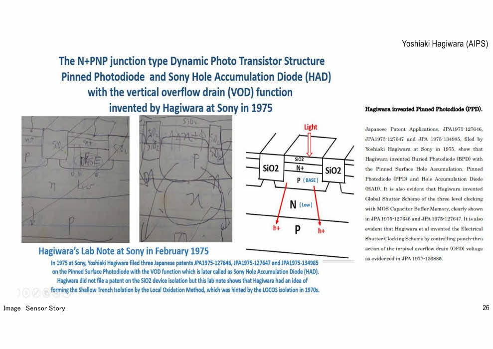
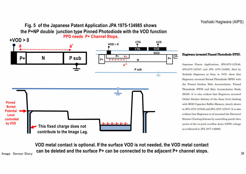
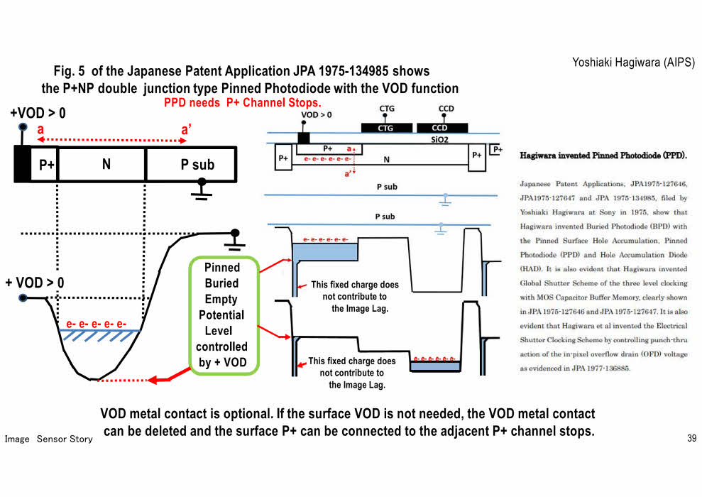
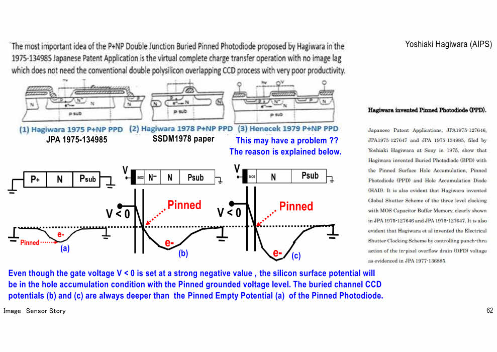
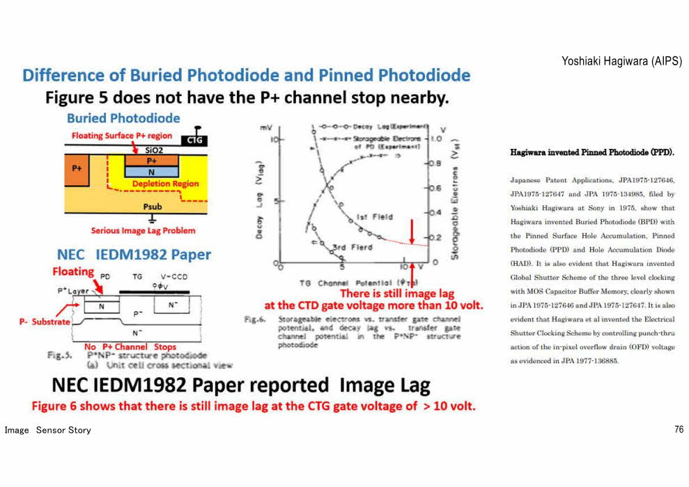
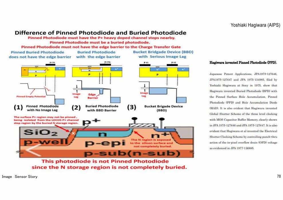
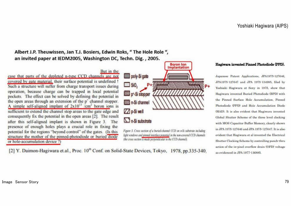
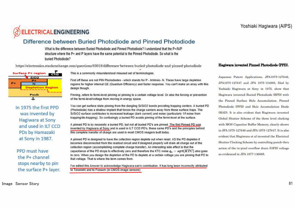
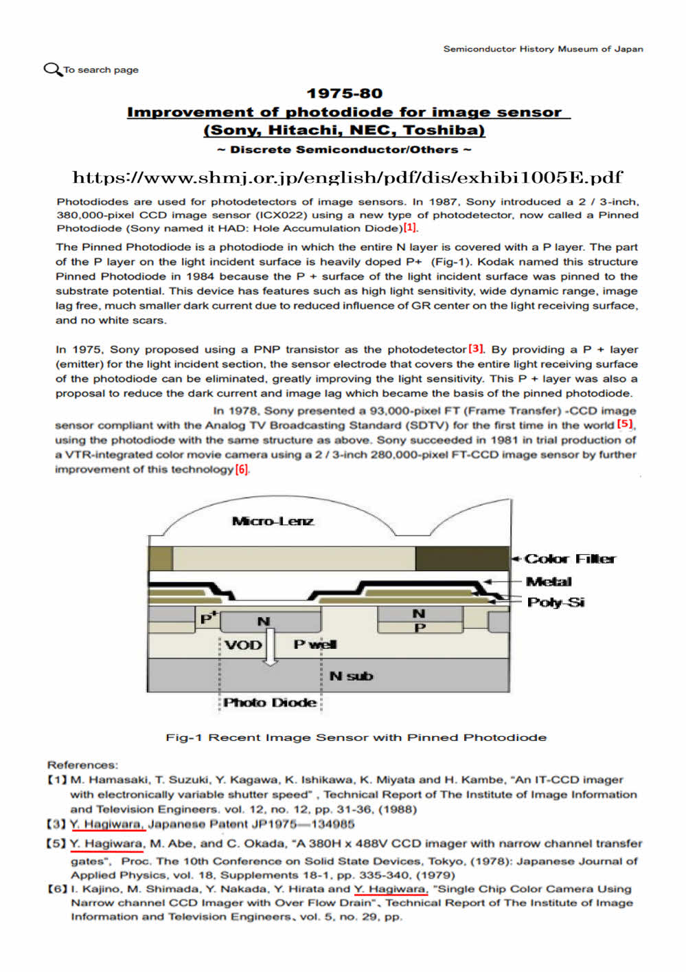
Pinned Photodiode is defined just as a Buried Photodiode
with a pinned surface majority carrier accumulation region
of the fixed and flat surface electrical potential
of no surface electric fileld
with
very low surface dark current.

The pinned surface potential also gives
the pinned empty potential
of the pinned buried charge collecting and storage region.

The pinned empty potential well implies
no image lag feature.

Pinned Photodiode is by necessity always Buried Photodiode.

But Buried Photodiode is not always Pinned Photodiode.

Buried Photodiode may have no pinned surface potential.

Buried Photodiode may have
a completely depleted surface potential
with a strong surface electric field
extended to the surface oxide.

The completely depleted surface potential
of Buried Photodiode
means that the floating surface potential
and the floating buried charge collecting and storage region
with the incomplete charge transfer of the image lag problem.

Hence Buried Photodiode may have the image lag problem
while Pinned Photodiode does not have
the image lag problem.

It is not well understood
that Buried Photodiode is not always Pinned Photodiode.

It is not well understood
the difference of Pinned Photodiode and Buried Photodiode.

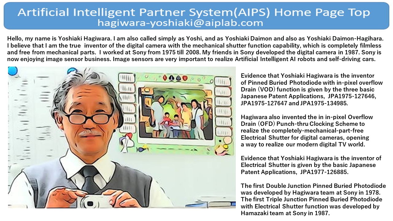
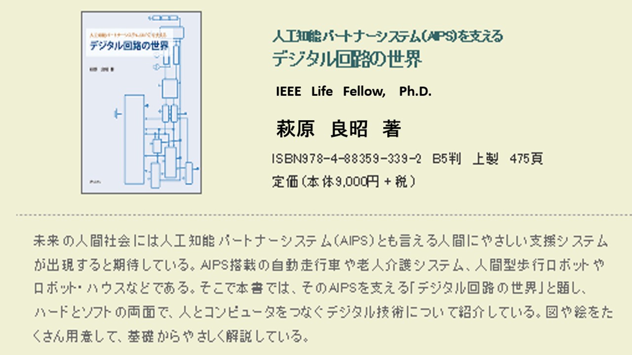
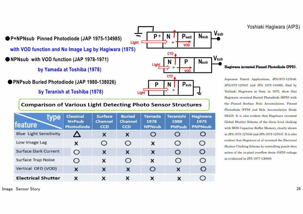
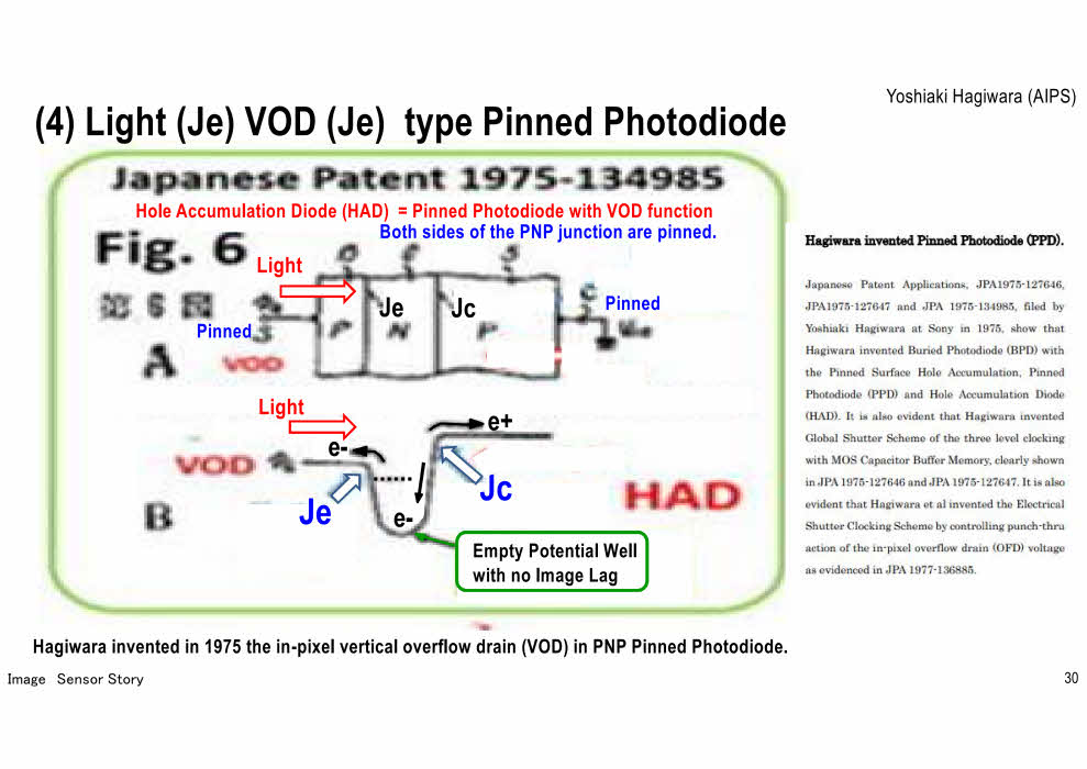
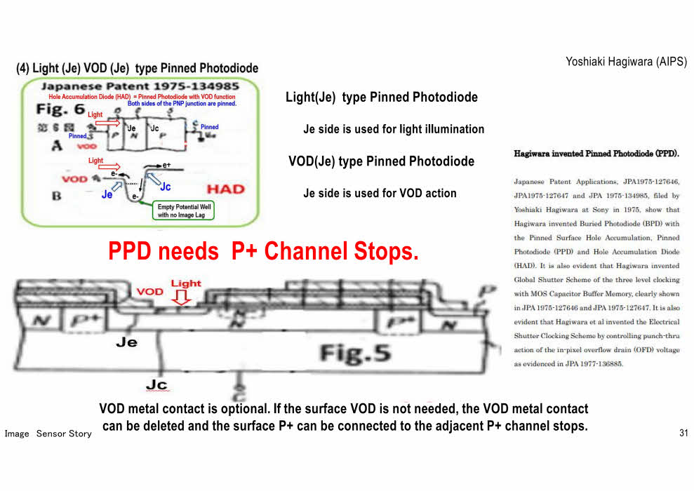
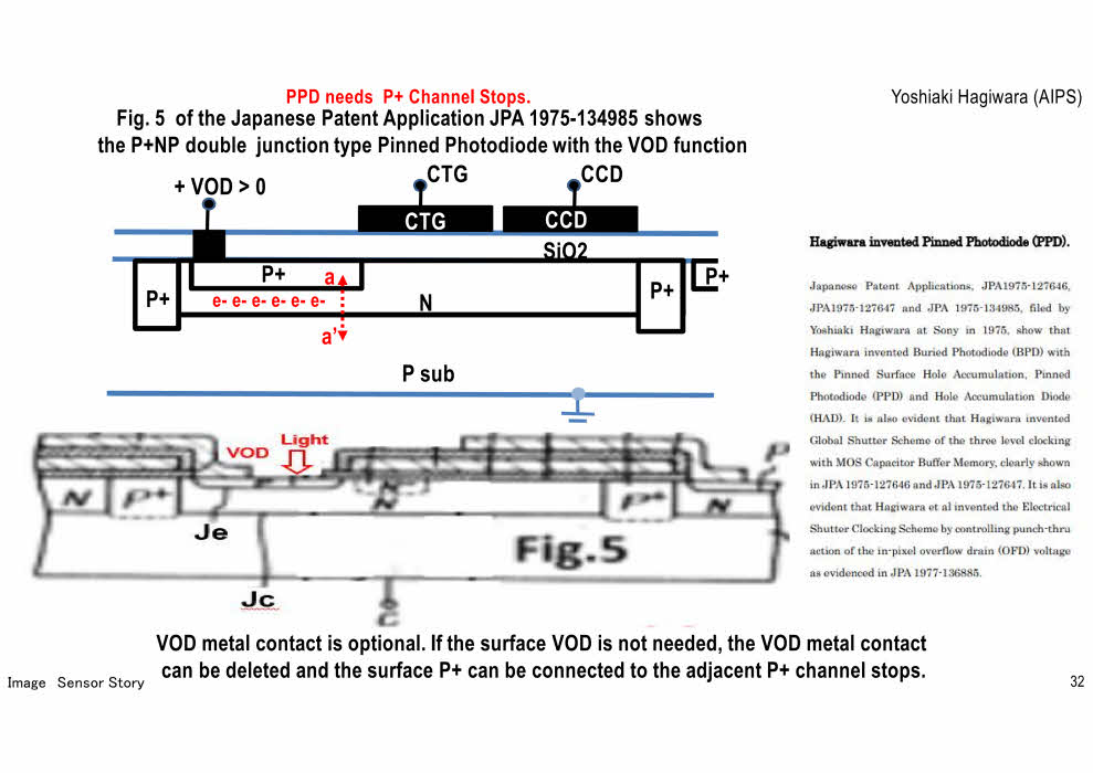
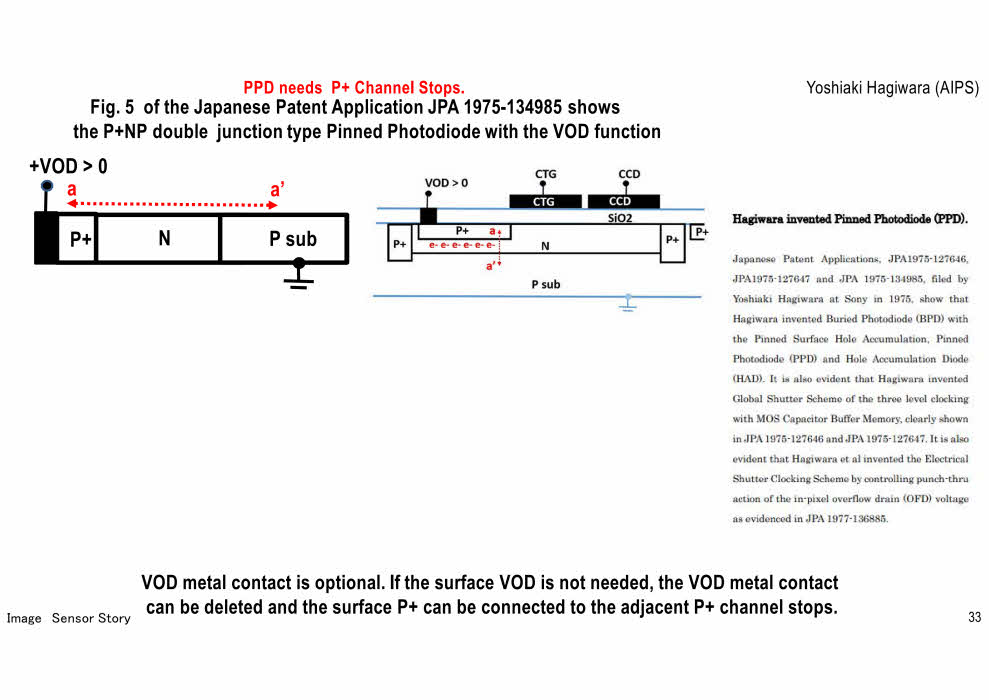
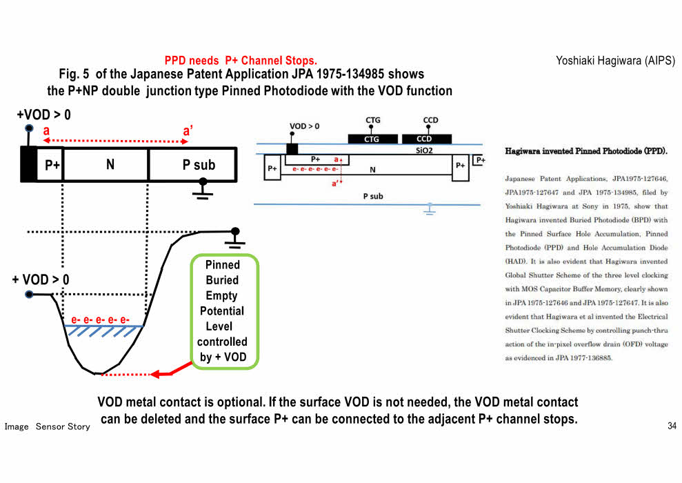
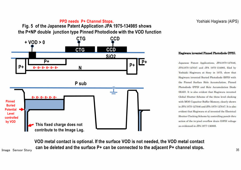
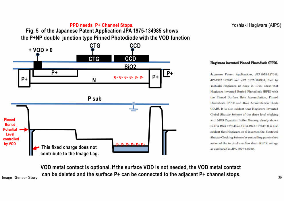
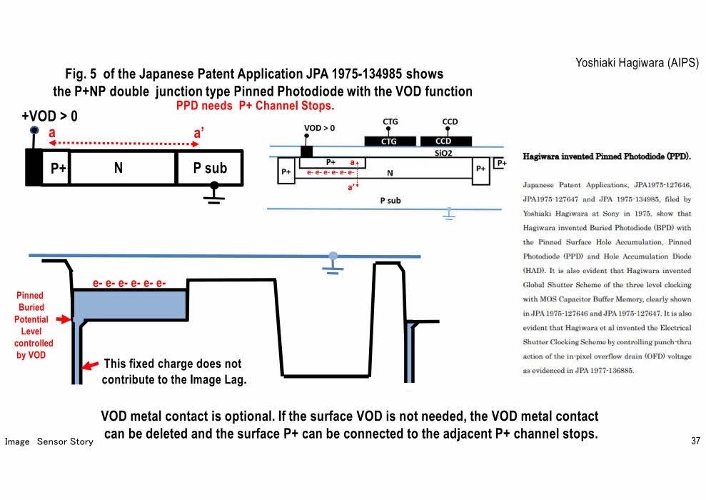
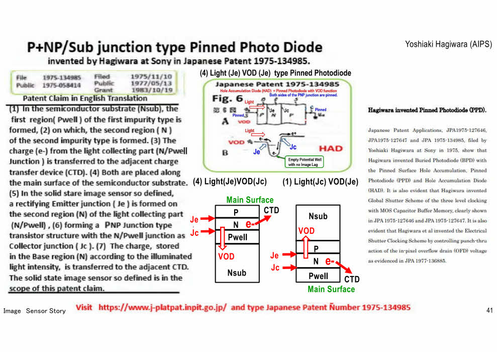
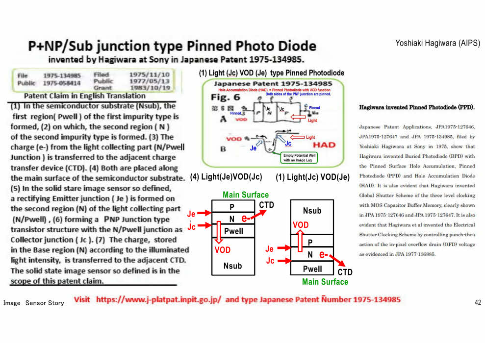
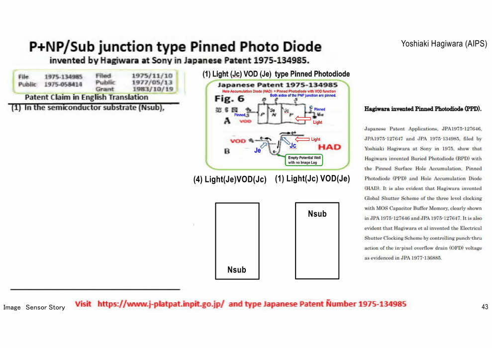
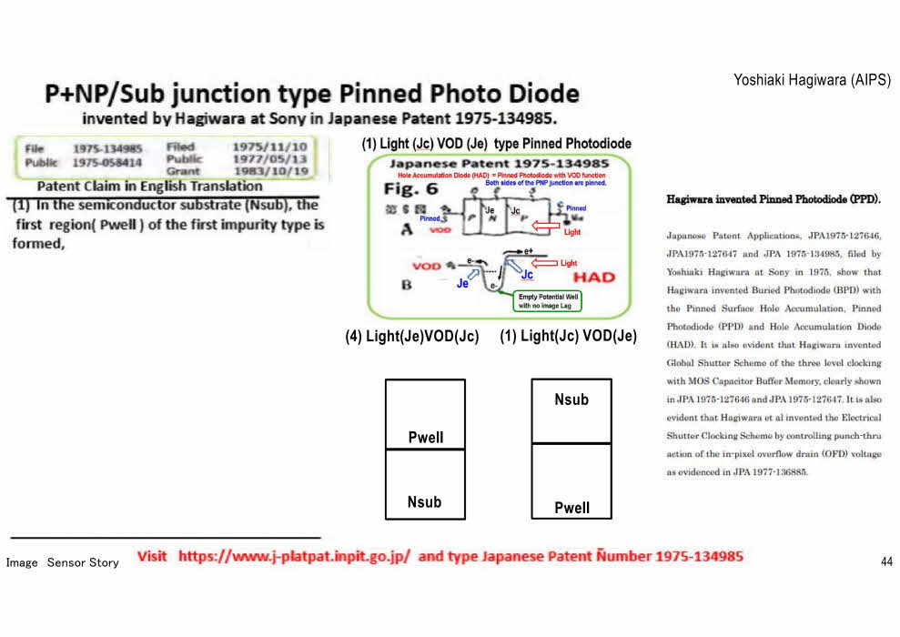
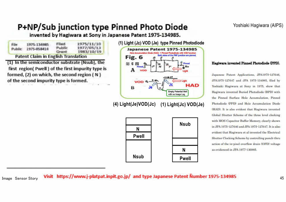
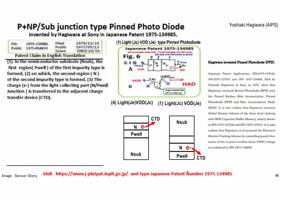
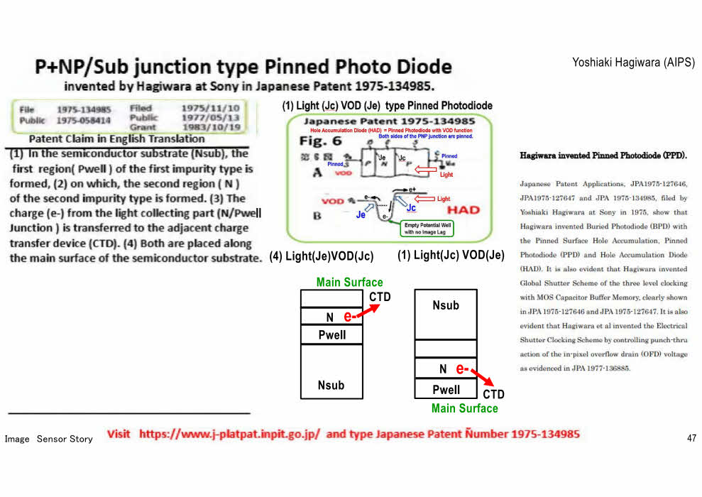
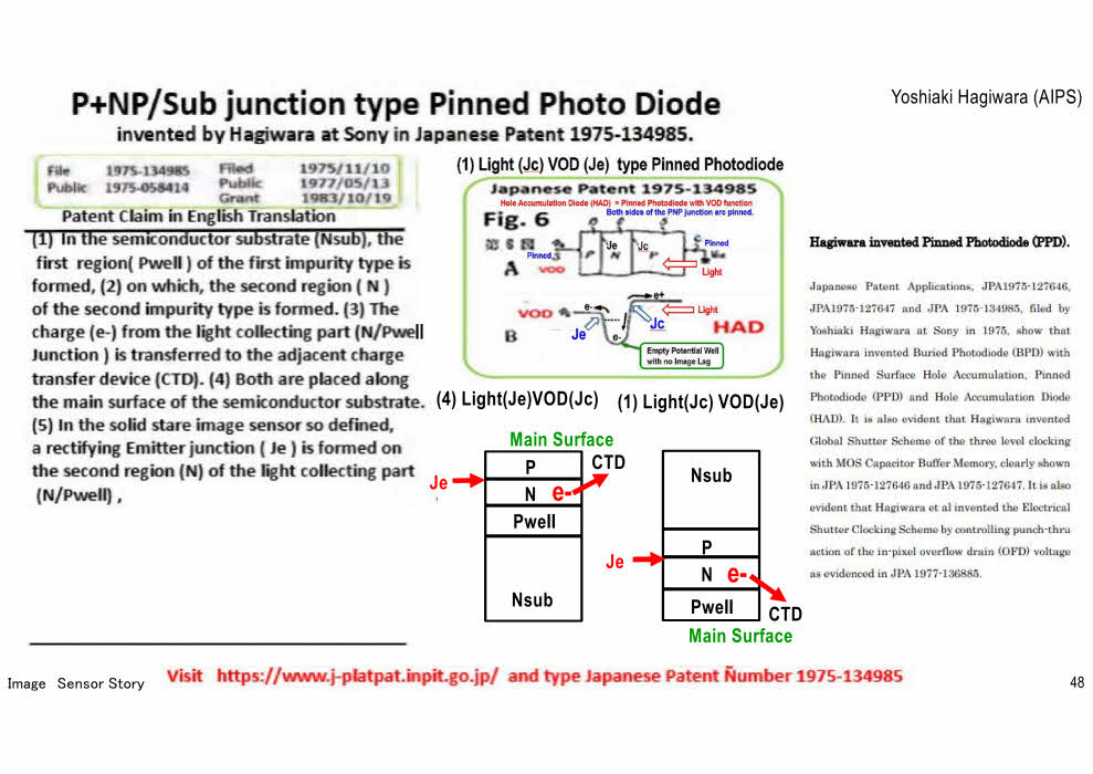
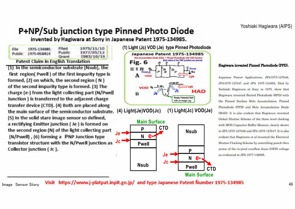
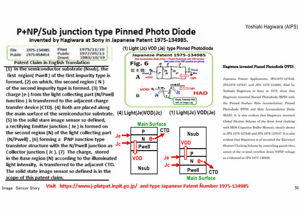
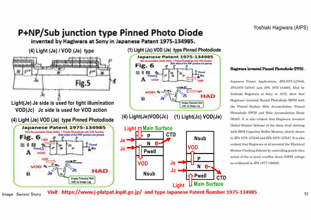
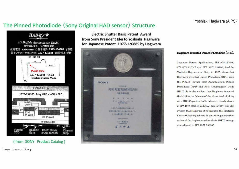
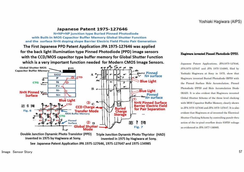
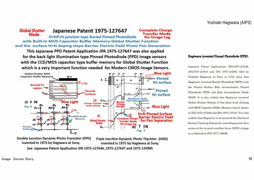
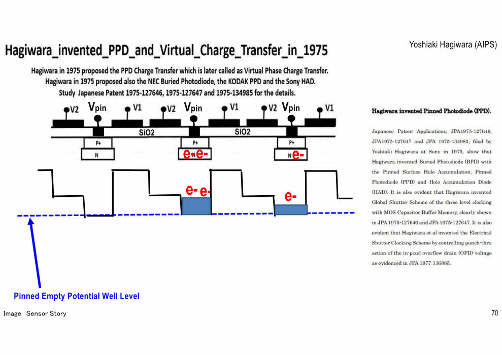
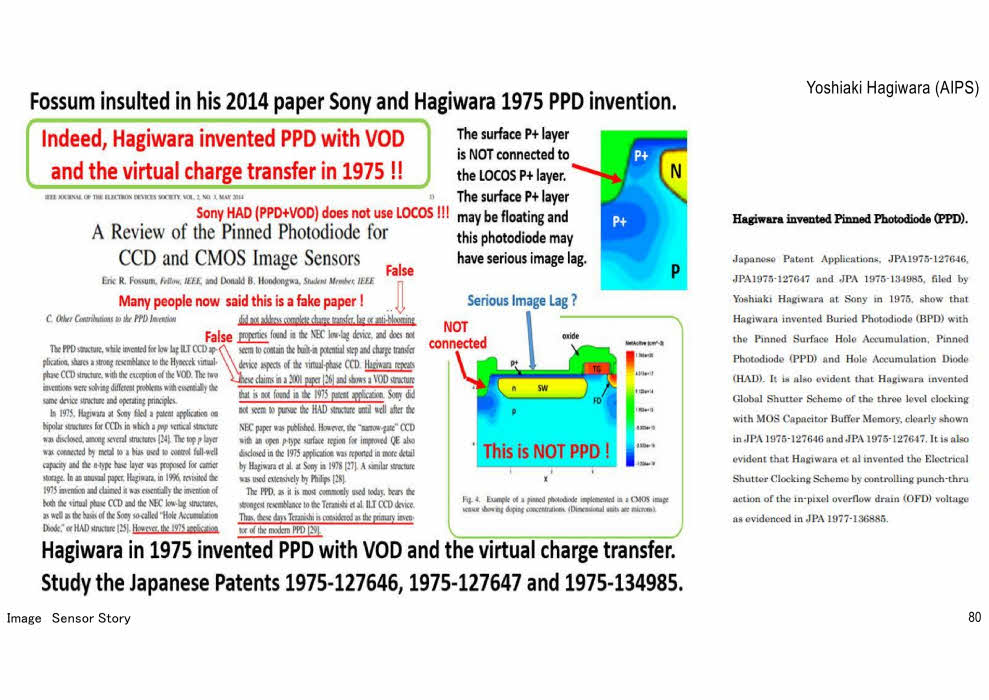
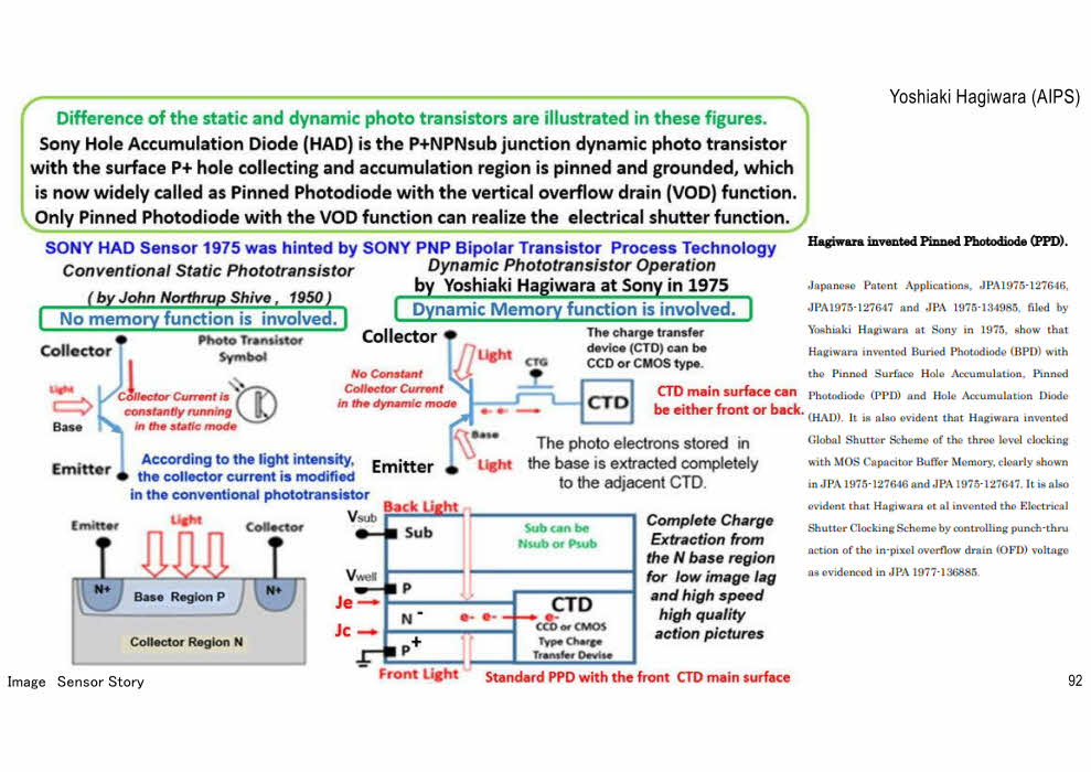
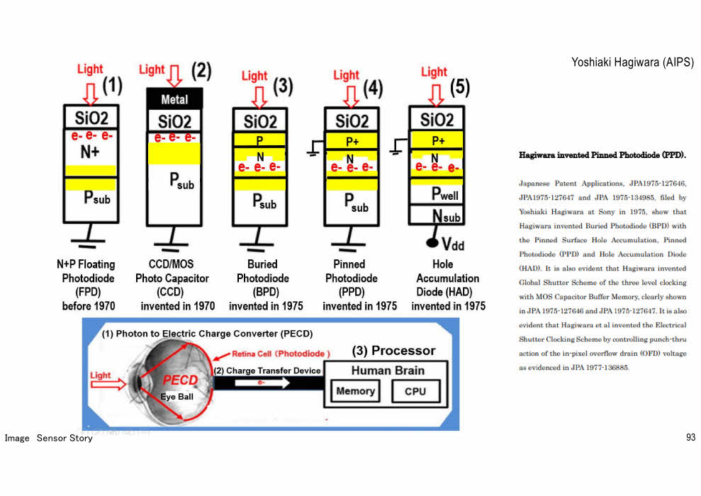
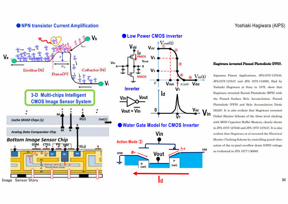
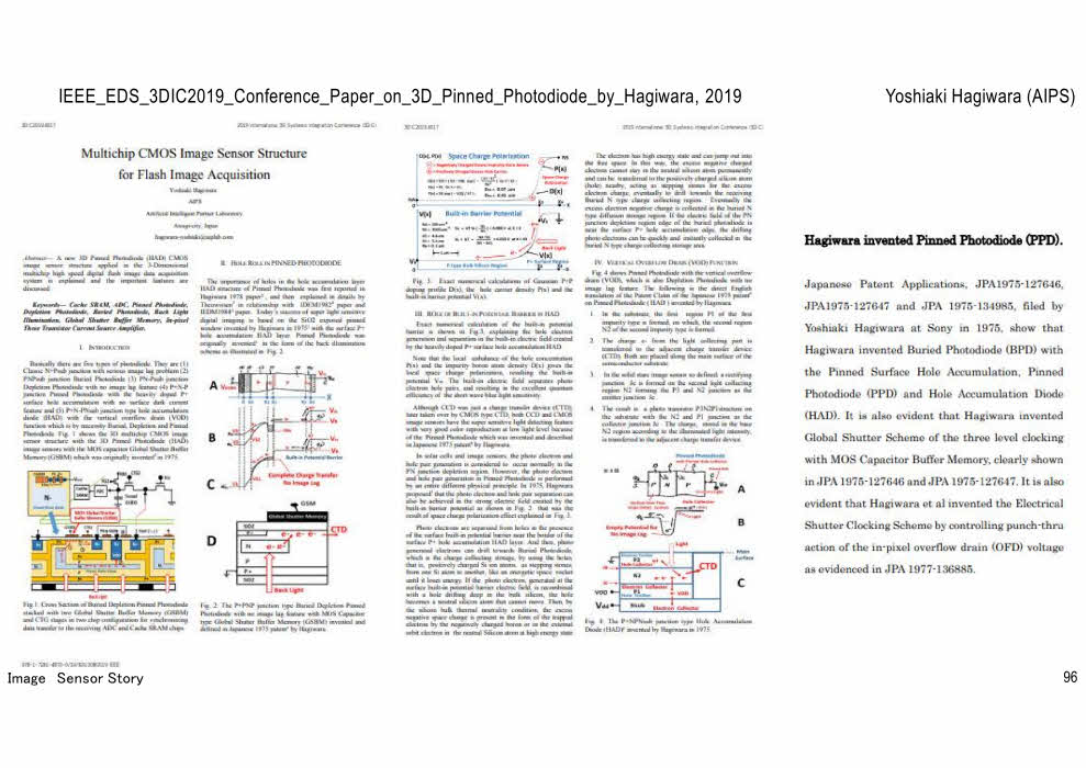
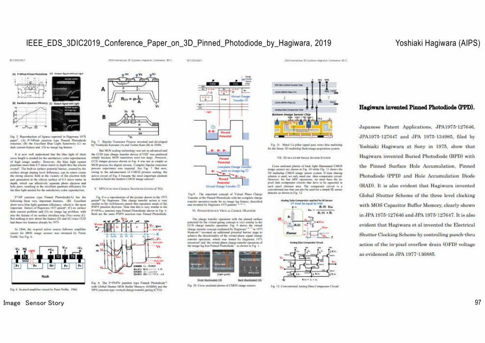
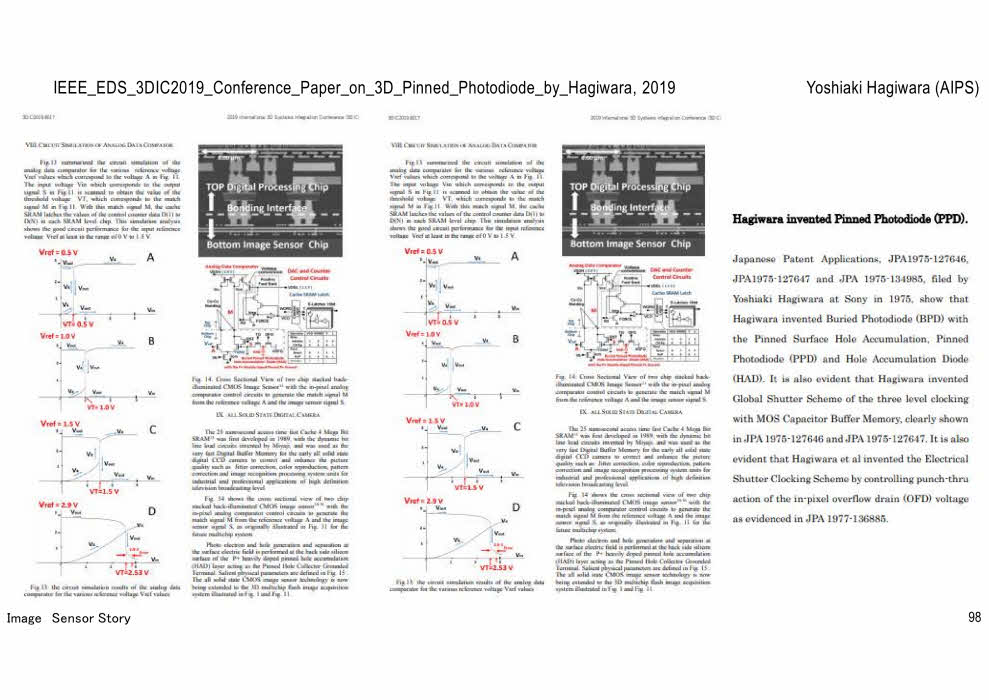
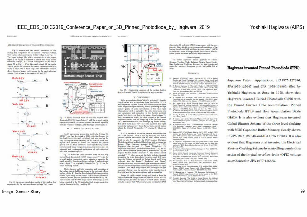
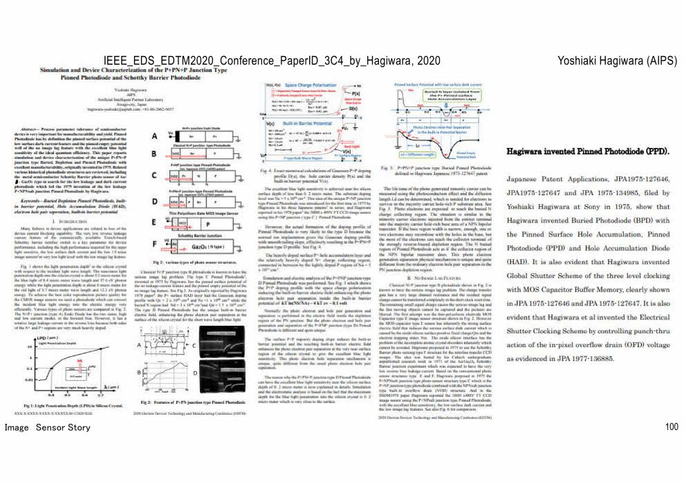
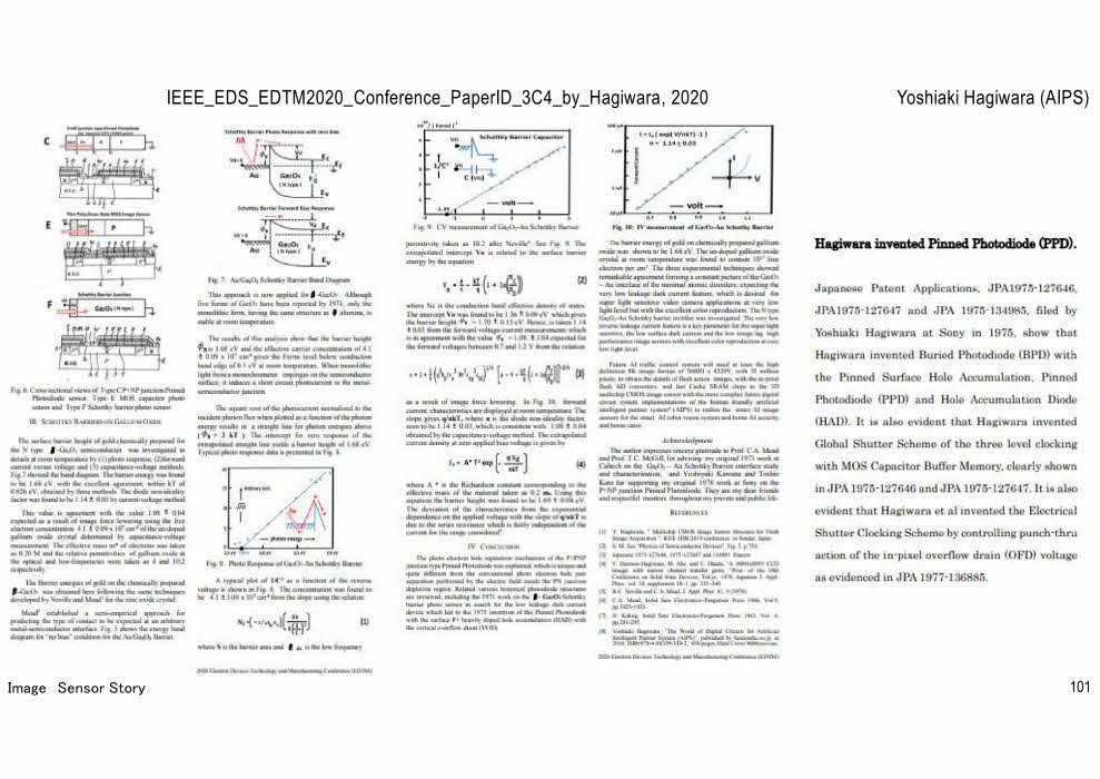
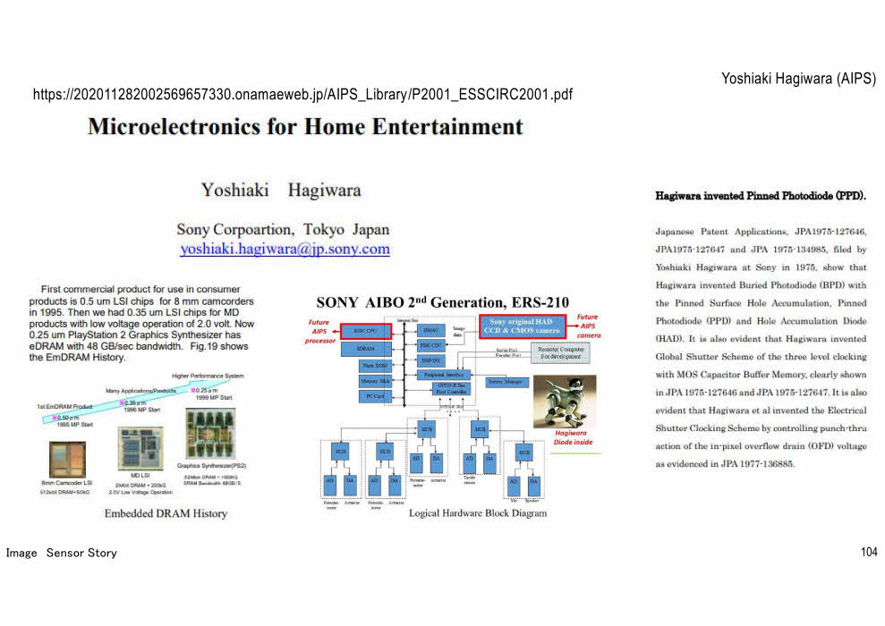
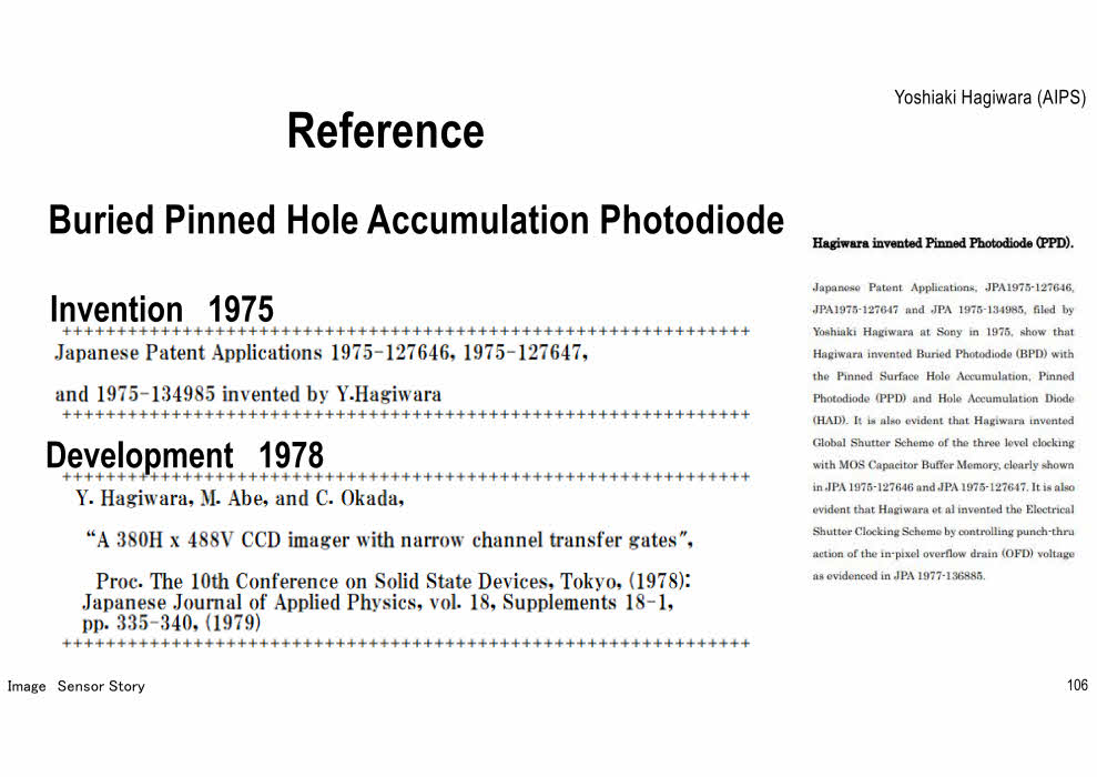
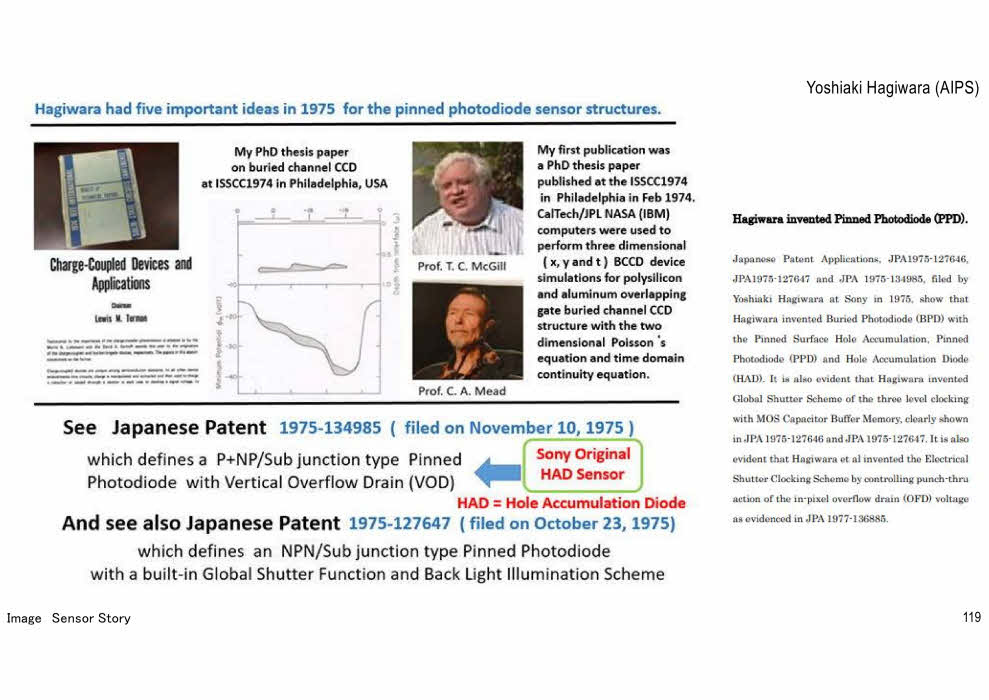
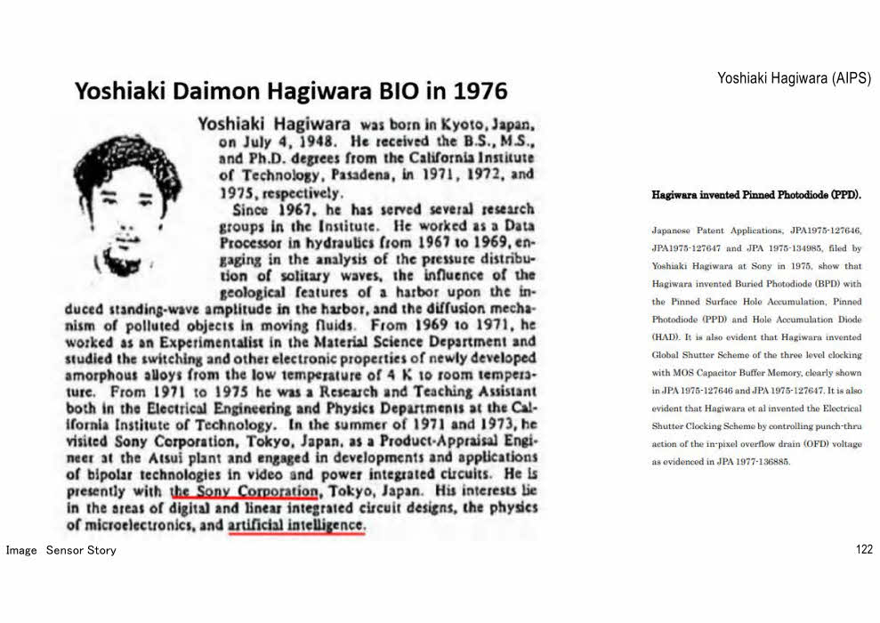
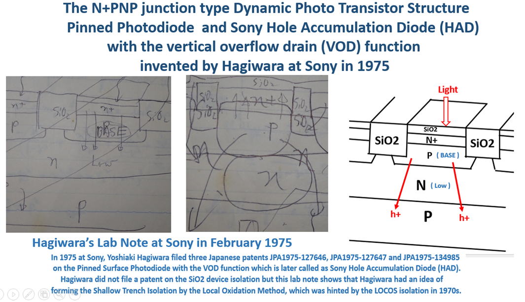
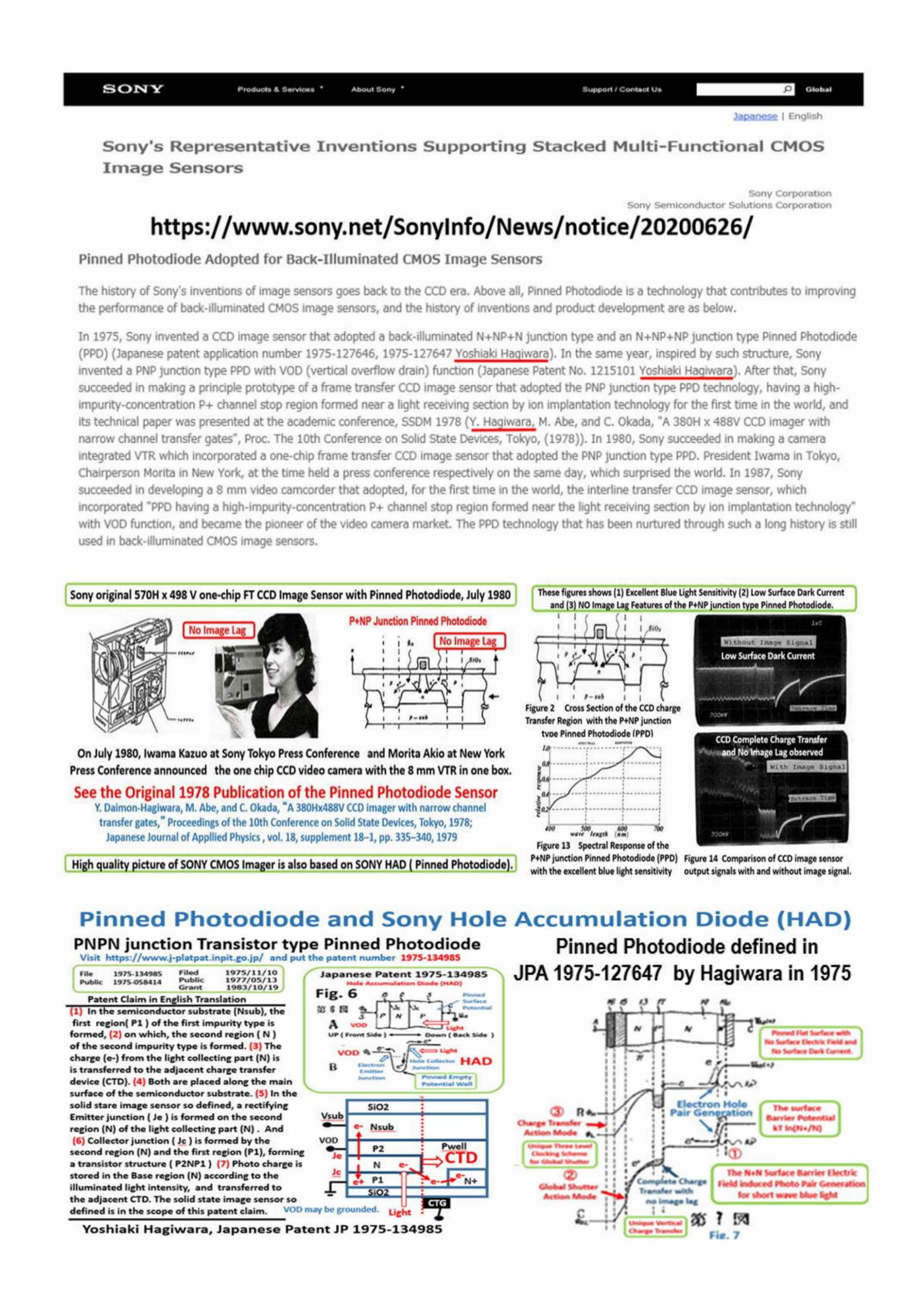
In either cases, Yoshiaki Hagiwara at Sony invented in 1975
both Buried Photodiode (BPD) ,
Pinned Photodiode(PPD),
and also Hole Accumulation Diode (HAD)
.

The evidence is given in the Japanese Patent Applicaitons

JPA 1975-127646

JPA 1975-127647

JPA 1975-134985, .

filed by Hagiwara at Sony in 1975.

show that Hagiwara invented Buried Photodiode (BPD),
Pinned Photodiode (PPD)
and Hole Accumulation Diode (HAD).

++++++++++++++++++++++++++++++++++++++++++++++++++++++++++++++++++++++++++

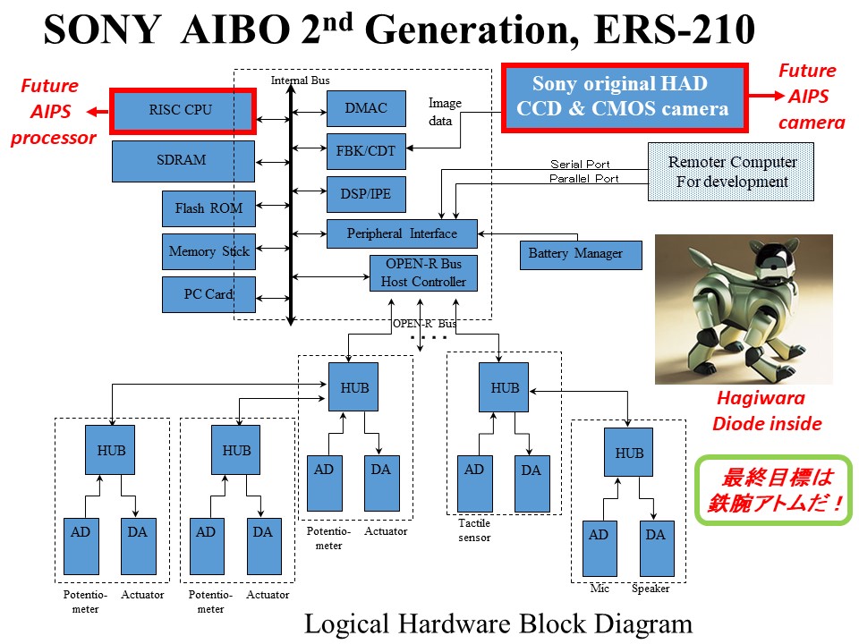
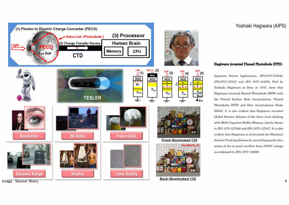
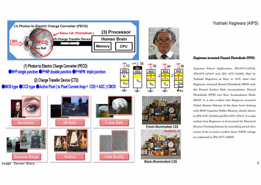
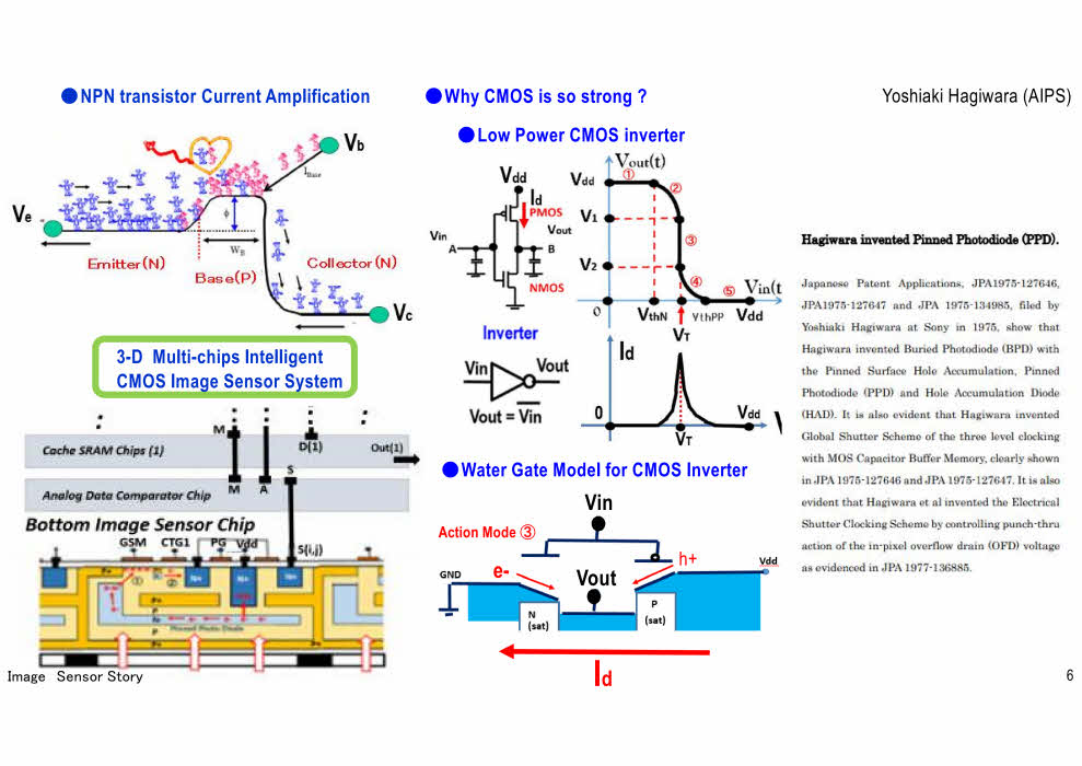
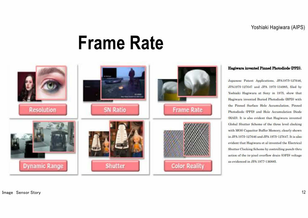
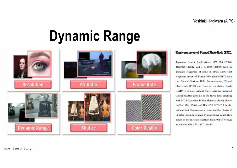
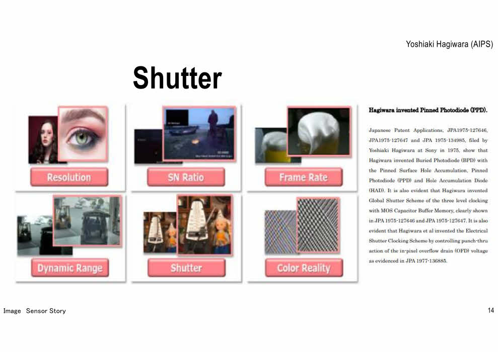
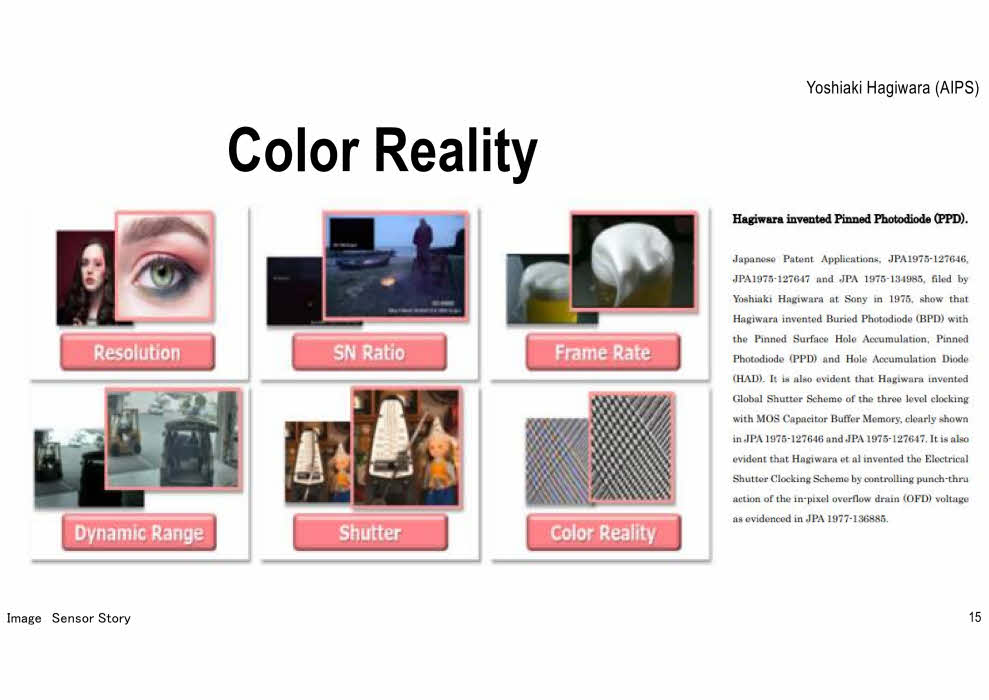
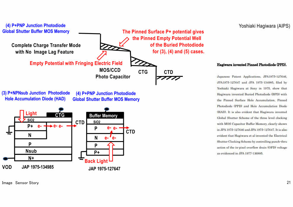
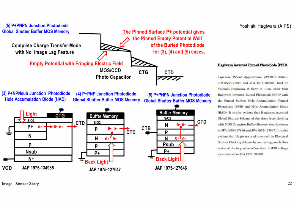
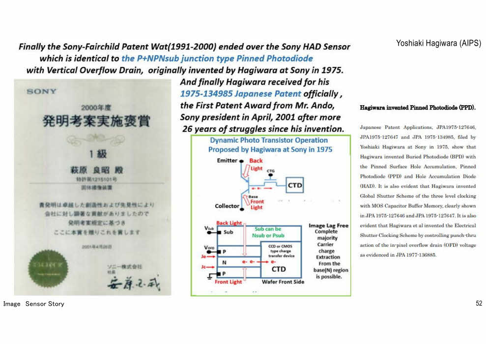
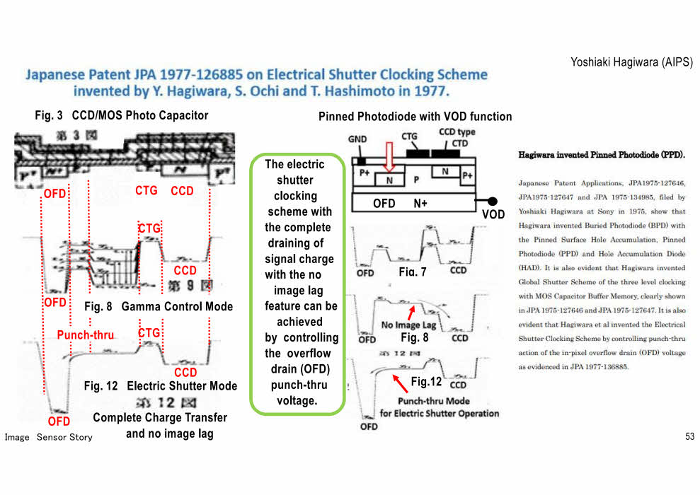
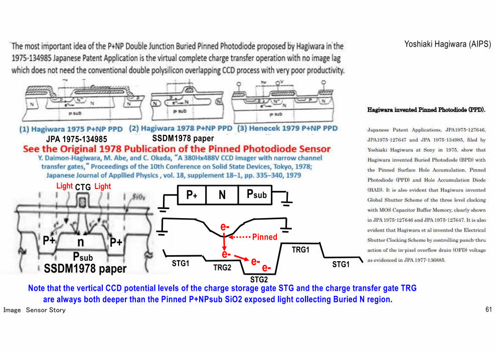
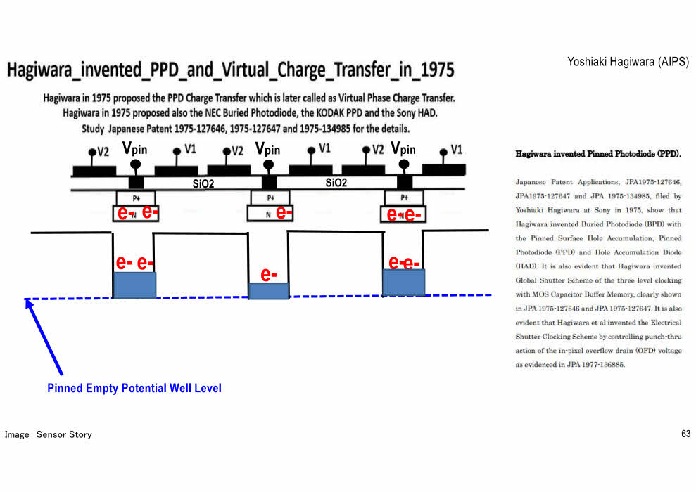
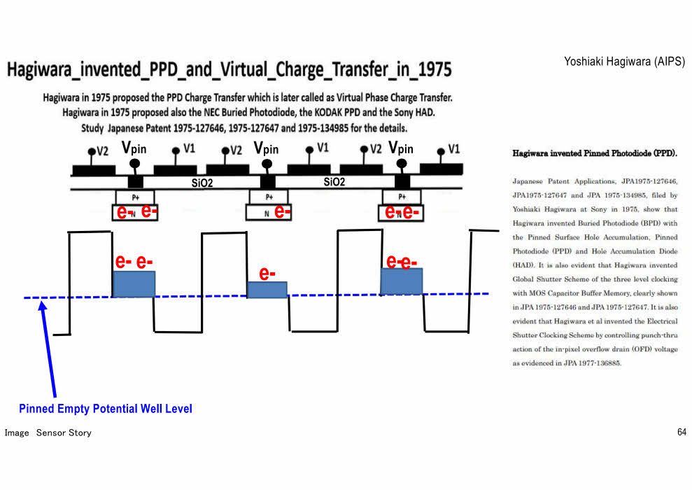
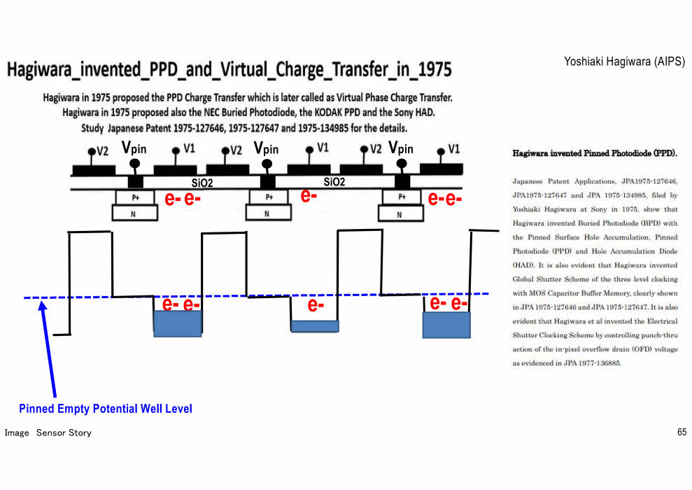
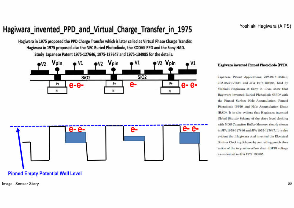
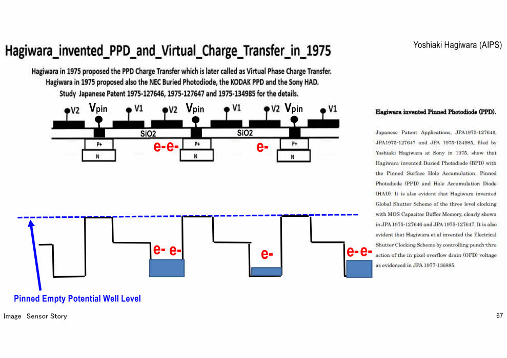
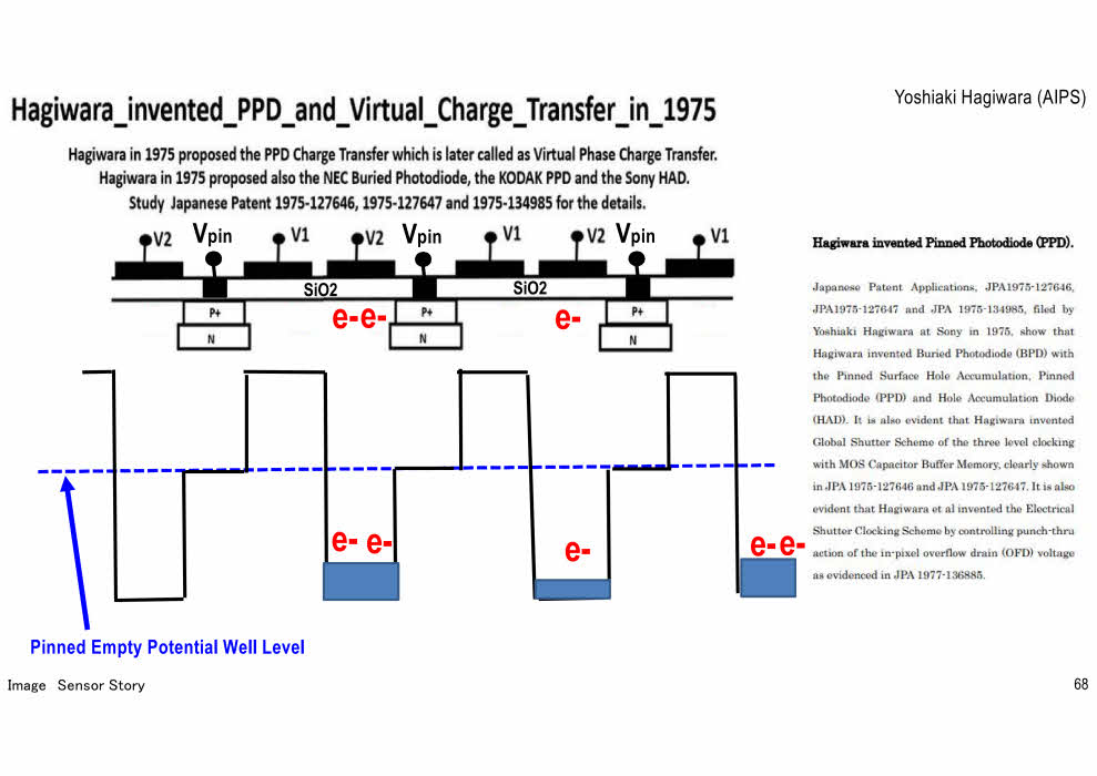
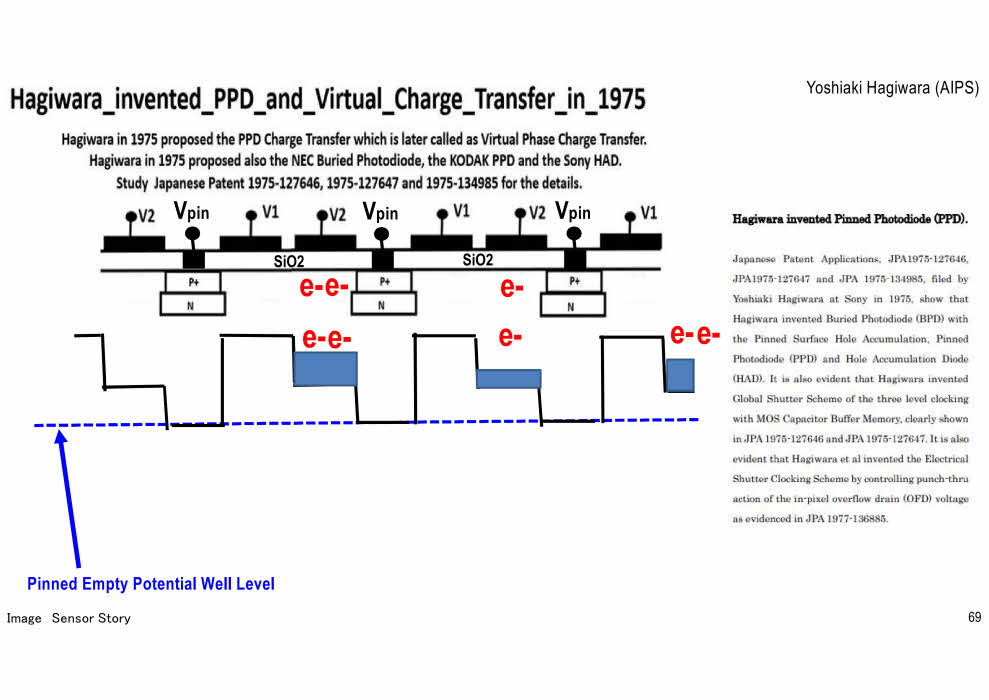
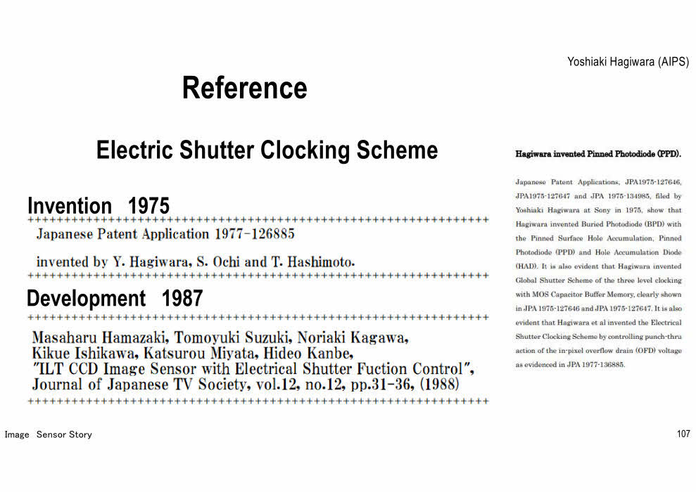
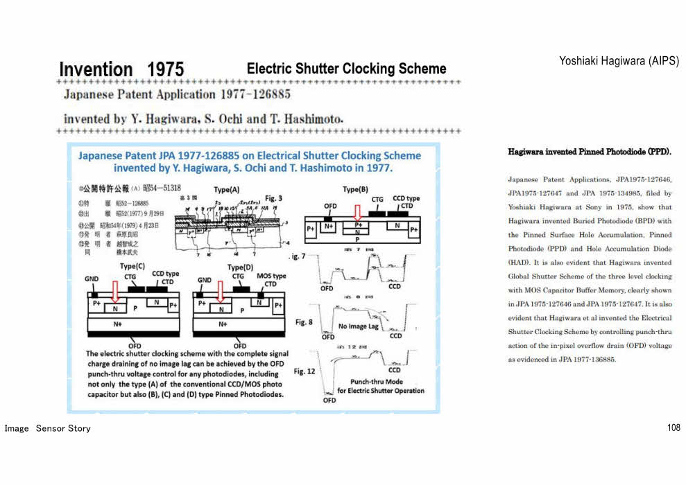
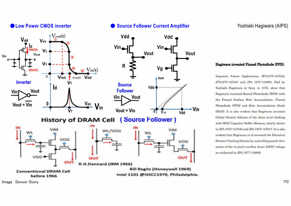
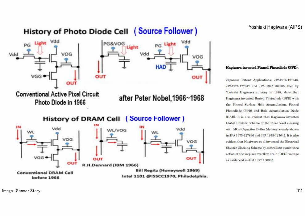
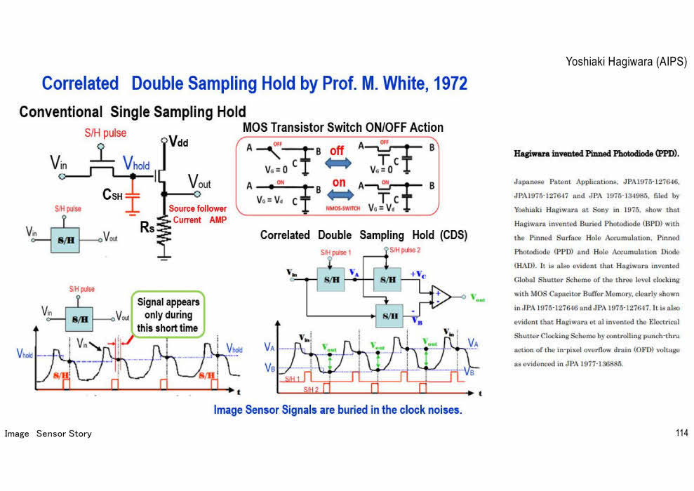
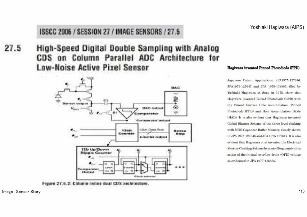
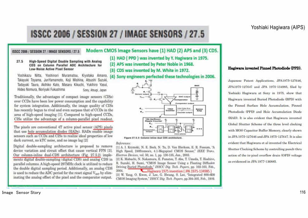
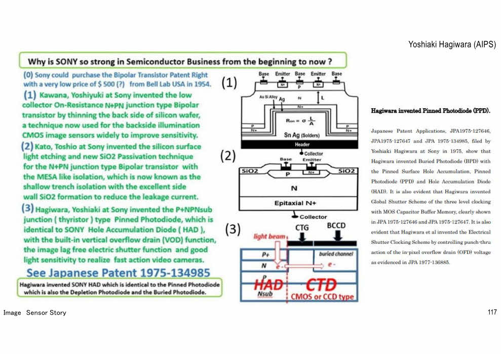
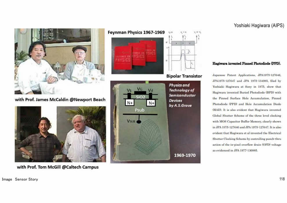
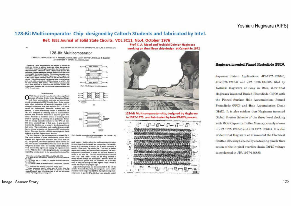
It is also evident in JPA 1975-127646 and JPA 1975-127647
that Hagiwara invented Global Shutter Scheme
of the three level clocking
with MOS Capacitor Buffer Memory.

It is also evident that Hagiwara et al invented
the Electrical Shutter Clocking Scheme
by controlling punch-thru action
of the in-pixel overflow drain (OFD) voltage
as evidenced in JPA 1977-136885.

++++++++++++++++++++++++++++++++++++++++++++++++++++++++++++++++++++++++++

Hagiwara published recently two IEEE EDS papers.

P2019_3DIC2019Paper_on_3D_Pinned_Photodiode.pdf


P2020_EDTM2020_PaperID_3C4_by_Hagiwara.pdf

MP4_Video_Presentation of EDTM2020_Paper is given below

P2020_EDTM2020_PaperID_3C4_by_Hagiwara.mp4

More details are explained below.

++++++++++++++++++++++++++++++++++++++++++++++++++++++++++++++++++++++++++


Image Sensor Story by Yoshiaki Hagiwara.pdf


Hagiwara_invented_PPD_and_Sony_HAD_in_1975.html

Hagiwara_invented_PPD_and_Sony_HAD_in_1975.pdf


The_First_Pinned_Photodiode_was_invented_in_1975_by_Yoshiaki_Hagiwar_at_Sony.pdf


++++++++++++++++++++++++++++++++++++++++++++++++++++++++++++++++++++++++++

Hagiwara Yoshiaki Lecture Notes for AIPS Robotics

++++++++++++++++++++++++++++++++++++++++++++++++++++++++++++++++++++++++++

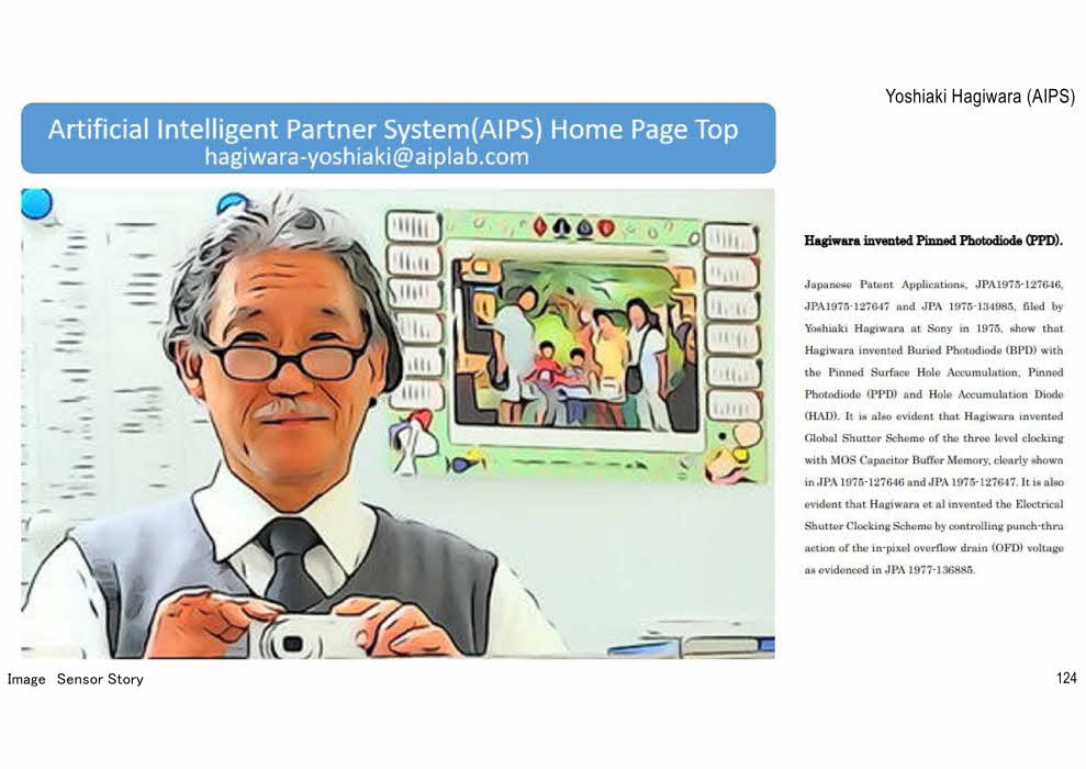
AIPS is the non-profit private organizaion (NPPO)

dedicated to produce scientific guide books and educational and introductory materials

devoted for the develpments of the Human Friendly Artificial Intelligent Partner System (AIPS),

AI Real Time Pattern Recognition Processors and Robotics Intelligent Vision Systems.


++++++++++++++++++++++++++++++++++++++++++++++++++++++++++++++


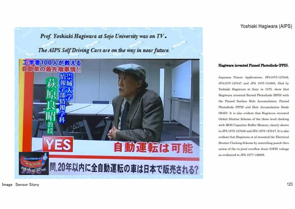
Yoshiaki Hagiwara was invited to talk about his dreams

in the international technical conferences .


https://imagesensors.org/

P1979_CCD79_in_Edinburgh_1979.pdf

https://www.esscirc-essderc2021.org/

http://www.aiplab.com/P2001_ESSCIRC2001.pdf 

http://www.aiplab.com/P2008_ESSCIRC2008Hagiwara.pdf 

http://isscc.org/

P2013_ISSCC2013PanelTalk.pdf

https://www.coolchips.org/


P2017_CoolChipsPanel170419.pdf


Yoshiaki Hagiwara also wrote papers about his works and dreams.


P1978_Pinned_Photodiode_1978_Paper_by_Hagiwara.pdf

P1996_Pinned_Photodidoe_used_in_Sony_1980_FT_CCD_Image_Sensor.pdf 

P2019_3DIC2019Paper_on_3D_Pinned_Photodiode.pdf 

P2020_EDTM2020_PaperID_3C4_by_Hagiwara.pdf
 

P2020_EDTM_PaperID_3C4_by_Hagiwara_MP4_Video_Presentation


These works were based on the following Japanese Patent Applications

that was never been desiclosed in details until recently

because of Hagiwara himself neglecting to appeal its importance.


JP1975-127646.pdf 

JP1975-127647.pdf 

JP1975-134985.pdf 

JP1977-126885.pdf 


++++++++++++++++++++++++++++++++++++++++++++++++++++++++++++++++


++++++++++++++++++++++++++++++++++++++++++++++++++++
On Nov 13, 2021, a Japanese Newspaper by Sangyou Times
wrote an aticle introducing Hagiwara.
++++++++++++++++++++++++++++++++++++++++++++++++++++

https://www.sangyo-times.jp/article.aspx?ID=5331


Future_of_Image_Sensors_and_Solar_Cells.pdf

Future_of_Image_Sensors_and_Solar_Cells.html

+++++++++++++++++++++++++++++++++++++++++++++


Sony_acknowledged_that_Hagiwara_invented_PPD_with_VOD_for_Electric_Shutter_Function

Semiconductor_History_Museum_of_Japan_also_supoorts_Hagiwara_1975_PPD_invention

Hagiwara_drew_the_Triple_Junction_Type_Pinned_Photodiode_in_his_1975_Lab_Note


++++++++++++++++++++++++++++++++++++++++++++++++++++++++++++++++
*********************************************************************
hagiwara-yoshiaki@aiplab.com for my activity at http://www.aiplab.com/
hagiwara@ssis.or.jp for my activity at http://www.ssis.or.jp/en/index.html

*********************************************************************


SSIS_Education_Activity ( Members Only )


SSIS_Education_GP_Activity_PR_MP4_01

SSIS_Education_GP_Activity_PR_MP4_02

SSIS_Education_GP_Activity_PR_MP4_03


Image_Sensor_Introduction_MP4_Video_for_AIPS_Robotics_by_Yoshiaki_Hagiwara


Image_Sensor_Story_Hagiwara_html ( Members Only )

*****************************


l


********************************************
AIPS Library
*******************************************

Yoshiaki Hagiwara wrote a book on
"the World of Artificial Intelligent Digital Circuits",
which is important and needed to built
the intelligent image sensor systems.

ISBM978-4-88359-339-2
Hard Cover, 460 page,
\ 9000 Japanese Yen + tax


If you are interestied in the book, Please visit

https://www.seizansha.co.jp/ISBN/ISBN978-4-88359-339-2.html

https://www.seizansha.co.jp/


++++++++++++++++++++++++++++++++++++++++++++++++++++++++++++++++++++++++++


++++++++++++++++++++++++++++++++++++++++++++++++++++++++++++++++

Gate Way to AIPS Library

++++++++++++++++++++++++++++++++++++++++++++++++++++++++++++++++

index_001_Enjoy_the_World_of_Hagiwara_Tomie_E_Tegami_Gallery.html

index_002_Enjoy_the_World_of_Hagiwara_Yoshiaki_Talks_and_Photo_Desk.html

index_003_Enjoy_the_World_of_Japanese_Short_Poem.html

index_004_Enjoy_the_World_of_Korean_Conversation.html

index_005_Enjoy_the_World_of_English_Conversation.html

index_006_Enjoy_the_World_of_Mathematics_Physics_and_Relativiry_Theory.html

index_007_Enjoy_the_World_of_Quantum_Mechanics_and_Semiconductor_Device_Physics.html

index_008_Enjoy_the_World_of_Artificial_Intelligent_Partner_System_AIPS_Digital_Circuits.html

index_009_Enjoy_the_World_of_Solid_State_Image_Sensors_and_PPD_Solar_Cells.html

index_010_Hagiwara_is_the_true_inventor_of_Pinned_Photodiode_PPD_and_Sony_HAD.html


++++++++++++++++++++++++++++++++++++++++++++++++++++++++++++++++


+++++++++++++++++++++++++++++++++++++++++++++++++++++++++++++++++++++++++++++

Hagiwara_invented_PPD_and_Sony_HAD_in_1975.pdf


+++++++++++++++++++++++++++++++++++++++++++++++++++++++++++++++++++++++++++++

001_Hagiwara_invented_PPD_and_Sony_HAD_in_1975.pdf

002_Image_Sensor_Story_by_Hagiwara.pdf

003_Future_of_Image_Sensors_and_Solar_Cells.pdf

004_The_First_Pinned_Photodiode_was_invented_in_1975_by_Yoshiaki_Hagiwar_at_Sony.pdf

+++++++++++++++++++++++++++++++++++++++++++++++++++++++++++++++++++++++++++++

++++++++++++++++++++++++++++++++++++++++++++++++++++++++++++++++++++++++++

What is the difference of Pinned Photodiode(PPD) and Buried Photodiode(BPD) ?

++++++++++++++++++++++++++++++++++++++++++++++++++++++++++++++++++++++++++

Buried Photodiode (BPD) was invented by Yoshiaki Hagiwara at sony in 1975
as a double junction type PNP photodiode.

JP1975-127646.pdf
JP1975-127647.pdf
JP1975-134985.pdf

However, Buried Photodiode(BPD) is not always Pinned Photodiode (PPD).

Buried Photodiode(BPD) may not have the Pinned surface p region.

Buried Photodiode(BPD) may have the serious image lag problem.

Buried Photodiode(BPD) may have the serious surface dark curent

when the surface is completely depleted and has the surface strong electric field


Pinned Photodiode (PPD) was also invented by Yoshiaki Hagiwara at Sony in 1975
in JPA 1975-127646 as a double junction type N+N-P+NP-P Buried Photodiode
and in JPA 1975-127647 as a triple junction type N+N-P+N Buried Photodiode
with the Pinned Surface N+N barrier electric field in the surface electron accumulation region
of the excellent short wave blue light sensitivity,
the very low surface dark current noise, and
the complete charge transfer capability of no image lag feature.

JP1975-127646.pdf

JP1975-127647.pdf

A triple junction type P+NPNsub Pinned Photodiode,
which is a double junction type P+NP Pinned Photodiode in the N type Silicon substrate Nsub,
was also invented in JPA 1975-134985 by Yoshiaki Hagiwara at Sony in 1975
with the built-in vertical overflow drain (VOD) capability.

JP1975-134985.pdf

Electrical Shutter Function Clocking Scheme
of controling the punch thru voltage of the built-in verical overflow drain (VOD)
was also invented in JPA 1975-126885 by Yoshiaki Hagiwara at Sony in 1977
and was applied in the triple junction type P+NPNsub Pinned Photodiode
which was named in 1987 as Hole Accumulation Diode(HAD) by Sony Hamazaki Team .

JP1977-126885.pdf

+++++++++++++++++++++++++++++++++++++++++++++++++++++++++++++++++++++++++++++++


+++++++++++++++++++++++++++++++++++++++++++++++++++++++++++++++++++++++++++++++

JP1977-837_Hitachi_Koike.pdf

JP1978-1971_Toshiba_Yamada_VOD_patent.pdf

JP1980-138026_NEC_Teranishi_Patent.pdf

+++++++++++++++++++++++++++++++++++++++++++++++++++++++++++++++++++++++++++++++

P1976_128_bit_Comparator.pdf

P1978_Pinned_Photodiode_1978_Paper_by_Hagiwara.pdf

P1979_CCD79_in_Edinburgh_1979.pdf

P1989_SONY_4MSRAM_1989.pdf

P1996_Pinned_Photodidoe_used_in_Sony_1980_FT_CCD_Image_Sensor.pdf

P2001_ESSCIRC2001.pdf

P2008_ESSCIRC2008Hagiwara.pdf

P2013_ISSCC2013PanelTalk.pdf

P2019_3DIC2019Paper_on_3D_Pinned_Photodiode.pdf

P2020_EDTM2020_PaperID_3C4_by_Hagiwara.pdf

P2020_Pinned_Photodiode_Solar_Cell_1.pdf

P2020_Pinned_Photodiode_Solar_Cell_2.pdf


+++++++++++++++++++++++++++++++++++++++++++++++++++++++++++++++++++++++++++++++

Buried_Photodiode_is_not_always_PPD_Hagiwara_Nov_2020.pdf

Difference_of_Pinned_Photodiode_and_Buiried_Photodiode.pdf

E-mail_Communication_on_Sony_Loral_Patent_War_1996.pdf

E-mail_communication_with_Albert_san_and_Yoshi.pdf

Evidence_that_Hagiwara_is_the_inventor_of_Pinned_Photodiode_2020_10_04a.pdf

Evidence_that_Hagiwara_is_the_inventor_of_Pinned_Photodiode_in_Japanese.pdf

Hagiwara_invented_PPD_and_Sony_HAD_in_1975.pdf

Hagiwara_invented_PPD_and_Sony_HAD_in_1975_2020_08_21.pdf

Hagiwara_invented_PPD_and_Sony_HAD_in_1975_Head.pdff

Image_Sensor_Story_07.pdf

Image_Sensor_Story_14.pdf

Origin_of_1975_Concept_of_Pinned_Photodiode.pdf

The_evidence_that_Hagiwara_is_the_inventor_of_Pinned_Photodiode_2020_10_02 .pdf


+++++++++++++++++++++++++++++++++++++++++++++++++++++++++++++++++++++++++++++++

Hagiwara_invented_PPD_and_Sony_HAD_in_1975.html

+++++++++++++++++++++++++++++++++++++++++++++++++++++++++++++++++++++++++++++++

AIPS Library
+++++++++++++++++++++++++++++++++++++++++++++++++++++++++++++++++++++++++++++++

Past Homepage Backups

2021_01_23

2020_12_22
2020_12_17
2020_12_15
2020_12_09

2020_06_27

2019_09_25
2019_07_12

2018_11_29


*********************************************************************

I really wish now to receive a chance to explain in public,
specially in the IEEE EDS community about the details of
my early pioneering works on image sensor invention
and development efforts. I devoted my life in Sony
for educating many young people, not only in Sony
but also universities and our competing companies.
They are the ones who made my dream come true now.

***************************************************************************
hagiwara-yoshiaki@aiplab.com for my activity at http://www.aiplab.com/
hagiwara@ssis.or.jp for my activity at http://www.ssis.or.jp/en/index.html

*********************************************************************