

++++++++++++++++++++++++++++++++++++++++++++++++++++++++++++++++
Gate Way to AIPS Library
++++++++++++++++++++++++++++++++++++++++++++++++++++++++++++++++
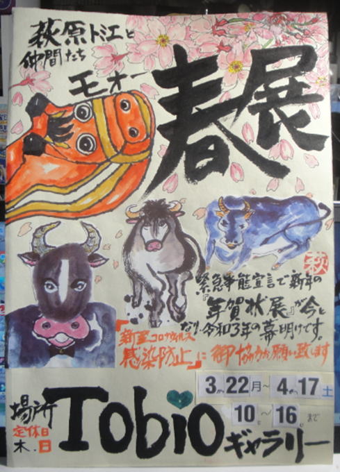
index_001_Enjoy_the_World_of_Hagiwara_Tomie_E_Tegami_Gallery.html
index_002_Enjoy_the_World_of_Hagiwara_Yoshiaki_Talks_and_Photo_Desk.html
index_003_Enjoy_the_World_of_Japanese_Short_Poem.html
index_004_Enjoy_the_World_of_Korean_Conversation.html
index_005_Enjoy_the_World_of_English_Conversation.html
index_006_Enjoy_the_World_of_Mathematics_Physics_and_Relativiry_Theory.html
index_007_Enjoy_the_World_of_Quantum_Mechanics_and_Semiconductor_Device_Physics.html
index_008_Enjoy_the_World_of_Artificial_Intelligent_Partner_System_AIPS_Digital_Circuits.html
index_009_Enjoy_the_World_of_Solid_State_Image_Sensors_and_PPD_Solar_Cells.html
index_010_Hagiwara_is_the_true_inventor_of_Pinned_Photodiode_PPD_and_Sony_HAD.html
++++++++++++++++++++++++++++++++++++++++++++++++++++++++++++++++
+++++++++++++++++++++++++++++++++++++++++++++++++++++++++++++++++++++++++++++
Hagiwara_invented_PPD_and_Sony_HAD_in_1975.pdf
+++++++++++++++++++++++++++++++++++++++++++++++++++++++++++++++++++++++++++++
001_Hagiwara_invented_PPD_and_Sony_HAD_in_1975.pdf
002_Image_Sensor_Story_by_Hagiwara.pdf
003_Future_of_Image_Sensors_and_Solar_Cells.pdf
004_The_First_Pinned_Photodiode_was_invented_in_1975_by_Yoshiaki_Hagiwar_at_Sony.pdf
+++++++++++++++++++++++++++++++++++++++++++++++++++++++++++++++++++++++++++++
++++++++++++++++++++++++++++++++++++++++++++++++++++++++++++++++++++++++++
What is the difference of Pinned Photodiode(PPD) and Buried Photodiode(BPD) ?
++++++++++++++++++++++++++++++++++++++++++++++++++++++++++++++++++++++++++
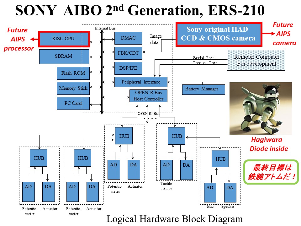
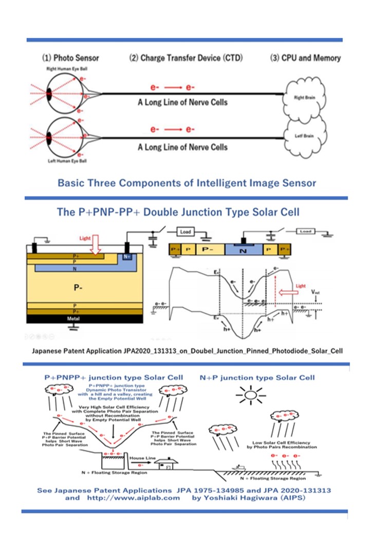
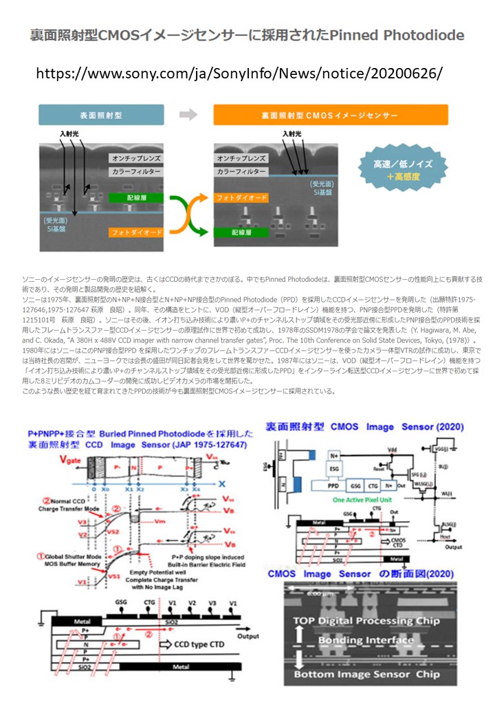
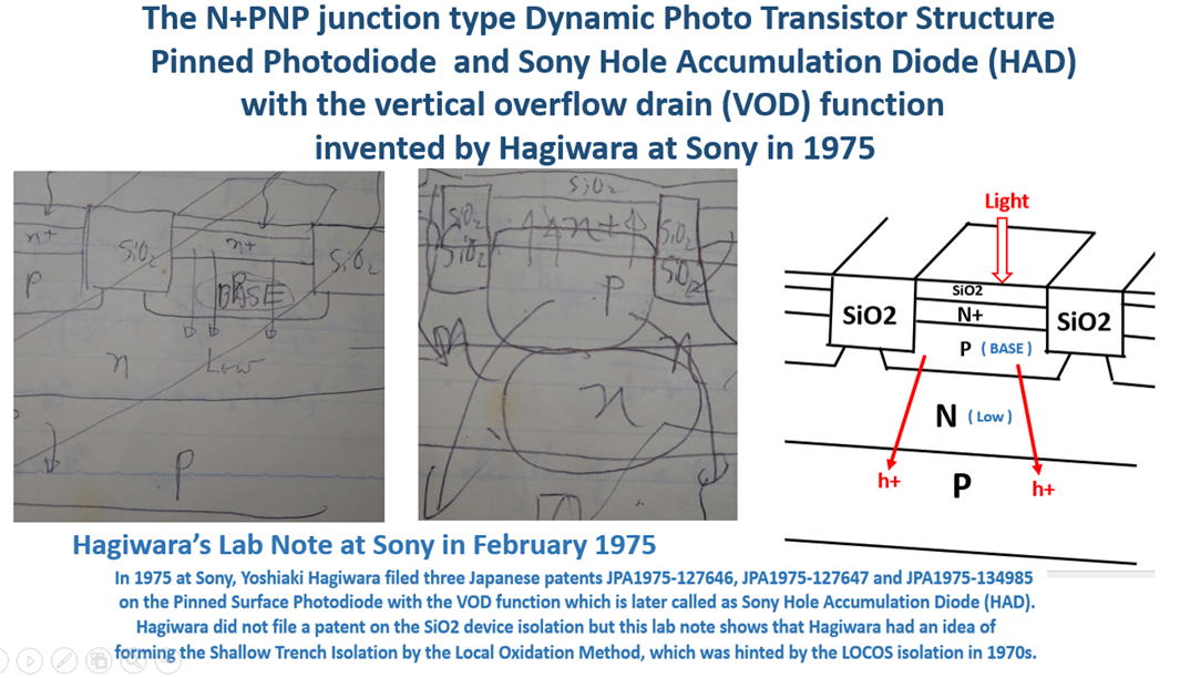
Buried Photodiode (BPD) was invented by Yoshiaki Hagiwara at sony in 1975
as a double junction type PNP photodiode.
JP1975-127646.pdf
JP1975-127647.pdf
JP1975-134985.pdf
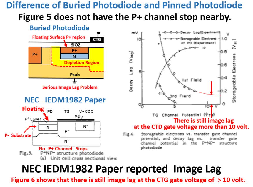
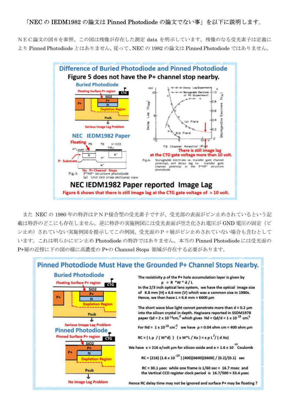
However, Buried Photodiode(BPD) is not always Pinned Photodiode (PPD).
Buried Photodiode(BPD) may not have the Pinned surface p region.
Buried Photodiode(BPD) may have the serious image lag problem.
Buried Photodiode(BPD) may have the serious surface dark curent
when the surface is completely depleted and has the surface strong electric field
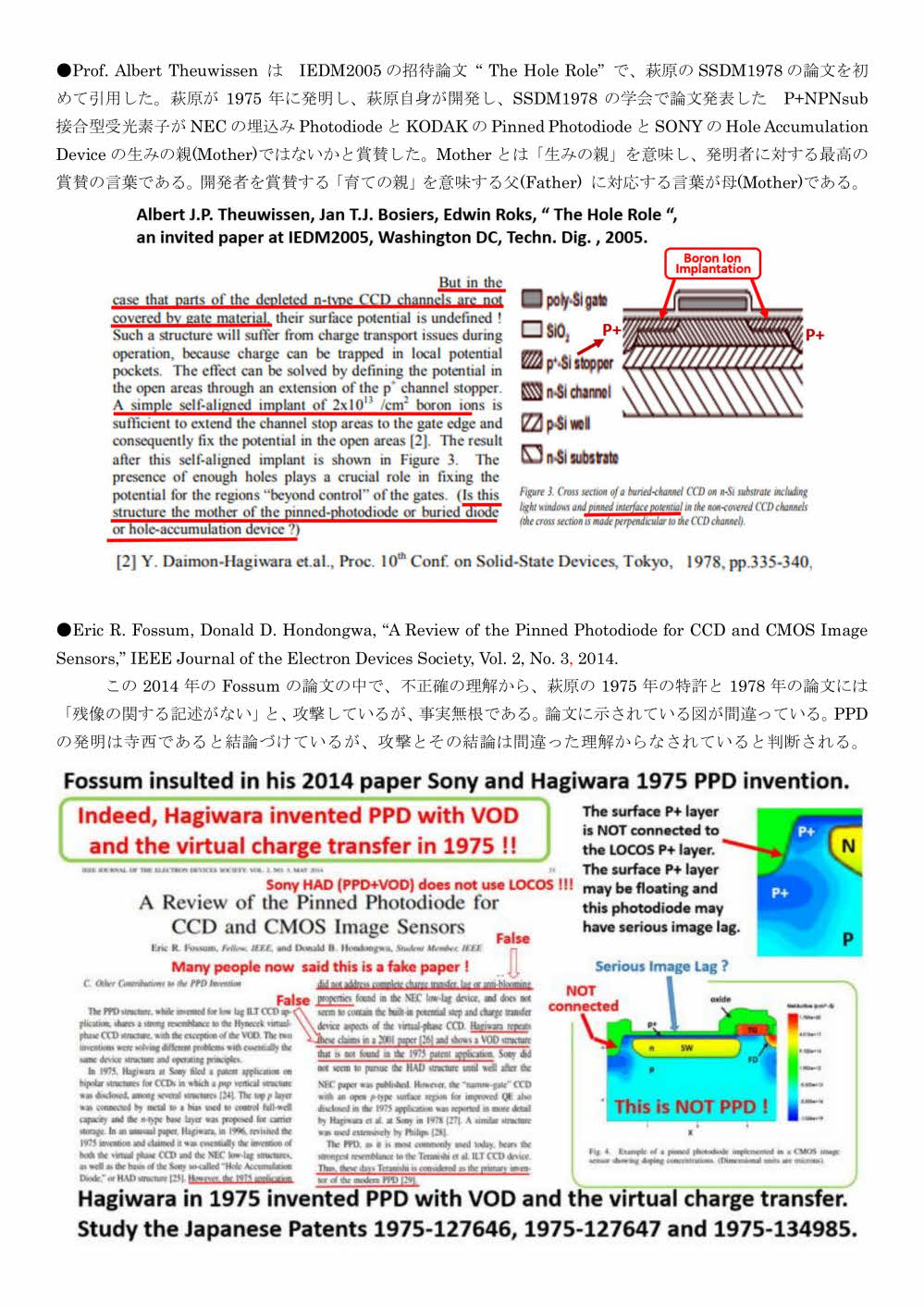
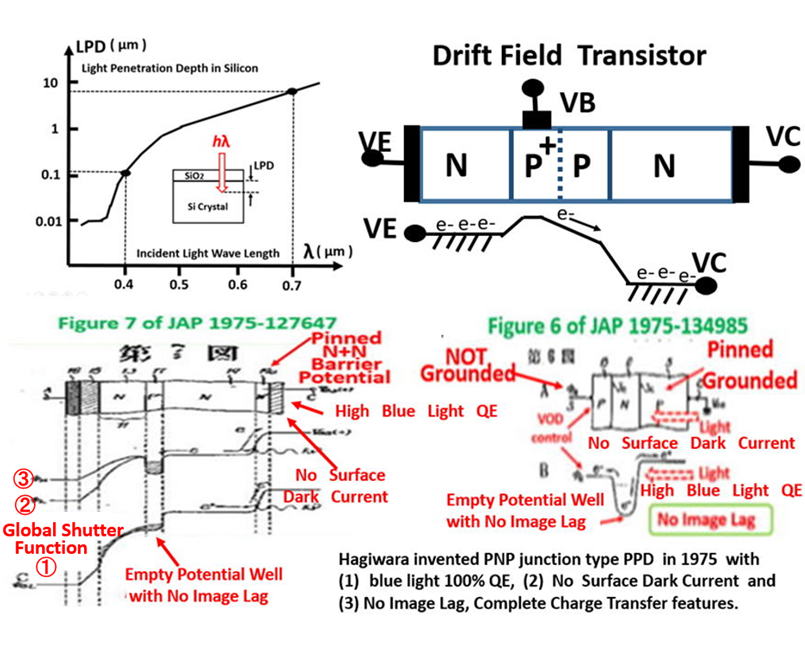
Pinned Photodiode (PPD) was also invented by Yoshiaki Hagiwara at Sony in 1975
in JPA 1975-127646 as a double junction type N+N-P+NP-P Buried Photodiode
and in JPA 1975-127647 as a triple junction type N+N-P+N Buried Photodiode
with the Pinned Surface N+N barrier electric field in the surface electron accumulation region
of the excellent short wave blue light sensitivity,
the very low surface dark current noise, and
the complete charge transfer capability of no image lag feature.
JP1975-127646.pdf
JP1975-127647.pdf
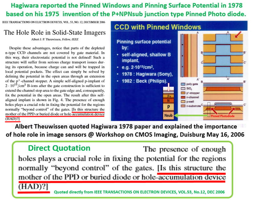
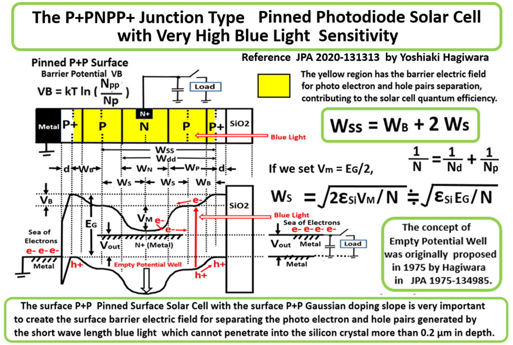
A triple junction type P+NPNsub Pinned Photodiode,
which is a double junction type P+NP Pinned Photodiode in the N type Silicon substrate Nsub,
was also invented in JPA 1975-134985 by Yoshiaki Hagiwara at Sony in 1975
with the built-in vertical overflow drain (VOD) capability.
JP1975-134985.pdf
Electrical Shutter Function Clocking Scheme
of controling the punch thru voltage of the built-in verical overflow drain (VOD)
was also invented in JPA 1975-126885 by Yoshiaki Hagiwara at Sony in 1977
and was applied in the triple junction type P+NPNsub Pinned Photodiode
which was named in 1987 as Hole Accumulation Diode(HAD) by Sony Hamazaki Team .
JP1977-126885.pdf
+++++++++++++++++++++++++++++++++++++++++++++++++++++++++++++++++++++++++++++++
+++++++++++++++++++++++++++++++++++++++++++++++++++++++++++++++++++++++++++++++
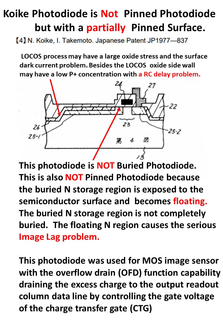
JP1977-837_Hitachi_Koike.pdf
JP1978-1971_Toshiba_Yamada_VOD_patent.pdf
JP1980-138026_NEC_Teranishi_Patent.pdf
+++++++++++++++++++++++++++++++++++++++++++++++++++++++++++++++++++++++++++++++
P1976_128_bit_Comparator.pdf
P1978_Pinned_Photodiode_1978_Paper_by_Hagiwara.pdf
P1979_CCD79_in_Edinburgh_1979.pdf
P1989_SONY_4MSRAM_1989.pdf
P1996_Pinned_Photodidoe_used_in_Sony_1980_FT_CCD_Image_Sensor.pdf
P2001_ESSCIRC2001.pdf
P2008_ESSCIRC2008Hagiwara.pdf
P2013_ISSCC2013PanelTalk.pdf
P2019_3DIC2019Paper_on_3D_Pinned_Photodiode.pdf
P2020_EDTM2020_PaperID_3C4_by_Hagiwara.pdf
P2020_Pinned_Photodiode_Solar_Cell_1.pdf
P2020_Pinned_Photodiode_Solar_Cell_2.pdf
+++++++++++++++++++++++++++++++++++++++++++++++++++++++++++++++++++++++++++++++
Buried_Photodiode_is_not_always_PPD_Hagiwara_Nov_2020.pdf
Difference_of_Pinned_Photodiode_and_Buiried_Photodiode.pdf
E-mail_Communication_on_Sony_Loral_Patent_War_1996.pdf
E-mail_communication_with_Albert_san_and_Yoshi.pdf
Evidence_that_Hagiwara_is_the_inventor_of_Pinned_Photodiode_2020_10_04a.pdf
Evidence_that_Hagiwara_is_the_inventor_of_Pinned_Photodiode_in_Japanese.pdf
Hagiwara_invented_PPD_and_Sony_HAD_in_1975.pdf
Hagiwara_invented_PPD_and_Sony_HAD_in_1975_2020_08_21.pdf
Hagiwara_invented_PPD_and_Sony_HAD_in_1975_Head.pdff
Image_Sensor_Story_07.pdf
Image_Sensor_Story_14.pdf
Origin_of_1975_Concept_of_Pinned_Photodiode.pdf
The_evidence_that_Hagiwara_is_the_inventor_of_Pinned_Photodiode_2020_10_02 .pdf
+++++++++++++++++++++++++++++++++++++++++++++++++++++++++++++++++++++++++++++++
Hagiwara_invented_PPD_and_Sony_HAD_in_1975.html
+++++++++++++++++++++++++++++++++++++++++++++++++++++++++++++++++++++++++++++++
AIPS Library
+++++++++++++++++++++++++++++++++++++++++++++++++++++++++++++++++++++++++++++++
Past Homepage Backups
2021_03_01
2021_01_23
2020_12_22
2020_12_17
2020_12_15
2020_12_09
2020_06_27
2019_09_25
2019_07_12
2018_11_29
++++++++++++++++++++++++++++++++++++++++++++++++++++++++++++++++
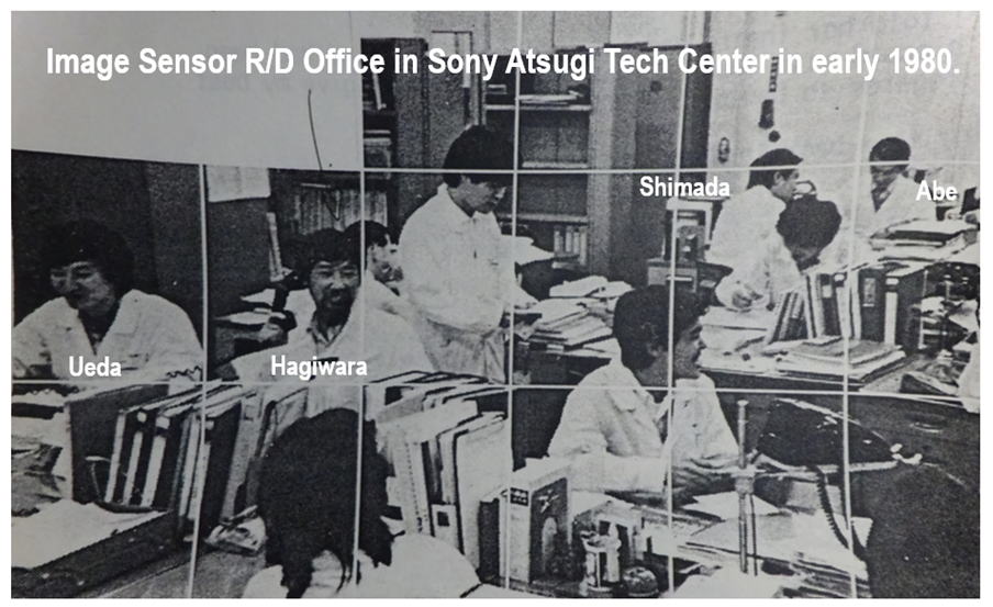
My Wonderful Memory Pictures
++++++++++++++++++++++++++++++++++++++++++++++++++++++++++++++++
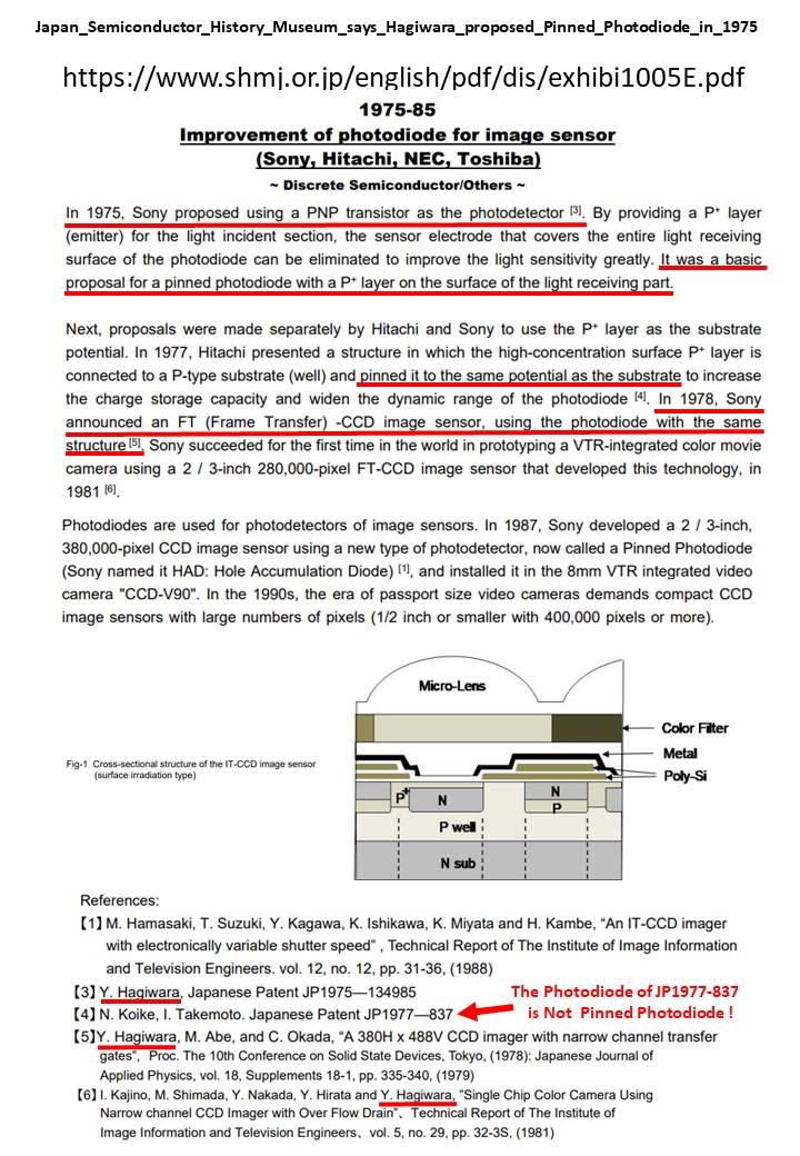
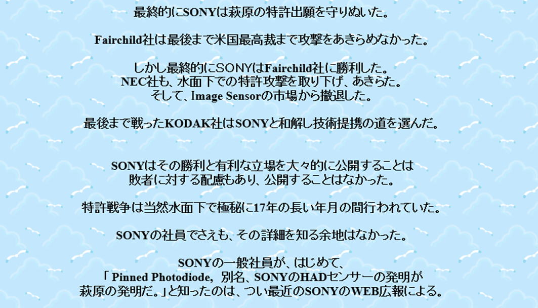
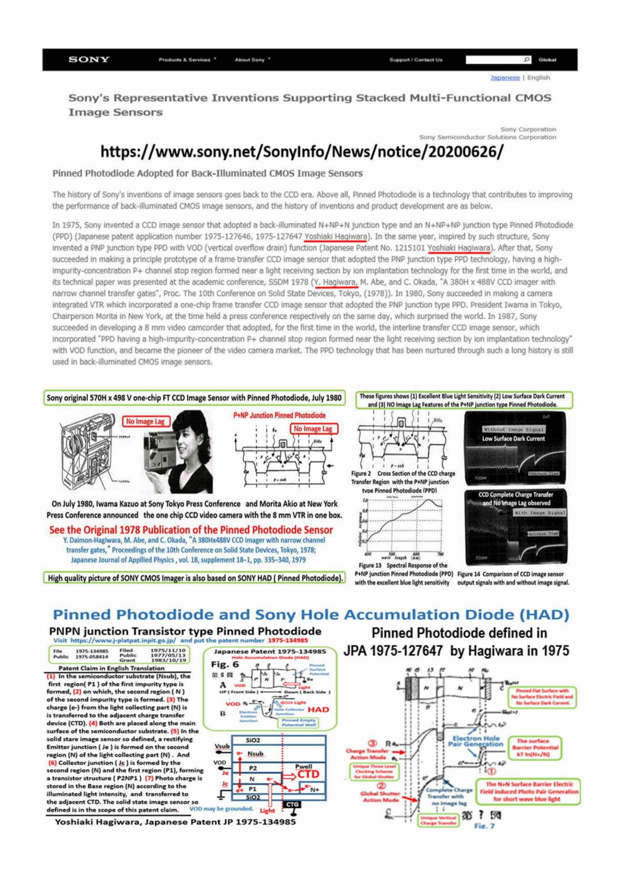
Hagiwara had to defend his 1975 Pinned Photodiode Basic Patents
JPA 1975-127646, JPA 1975-127647 and JPA 1975-134985
from Faircild, NEC and Kodack Patent Attacks
more than 15 years from 1990 till 2015.
Sony won the Farichi/Sony Patent War in 2000.
NEC gave up patent disputes and stopped image sesnor business.
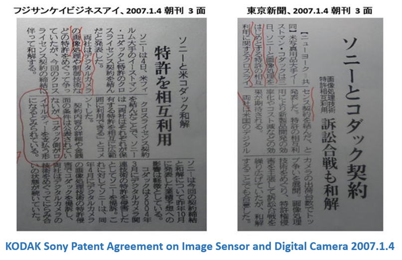
Sony and Kodak made a friendly technical cross liscence mutual agreement.
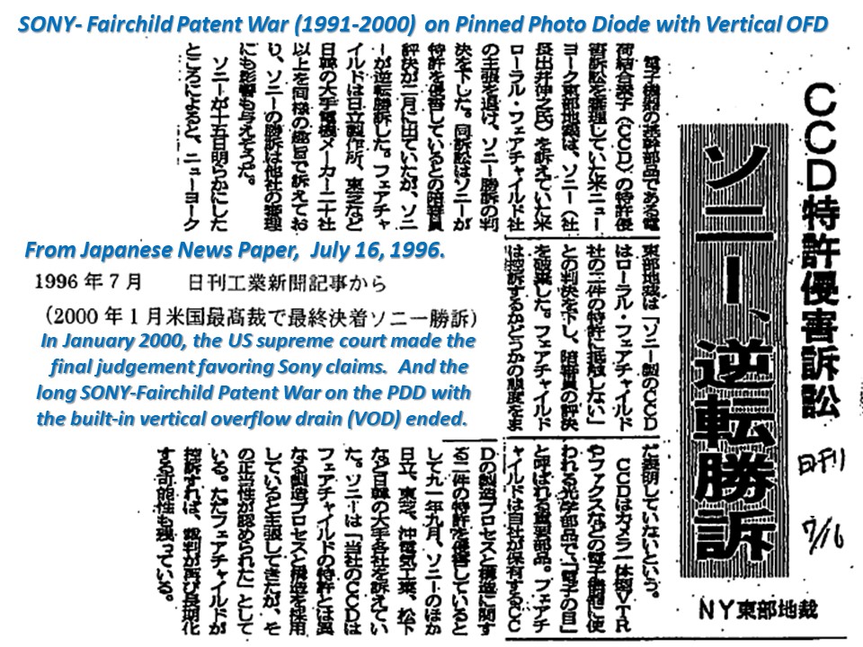
Sony and Kodak made a friendly technical cross liscence mutual agreement
while NEC gave up patent disputes and stopped image sesnor business..
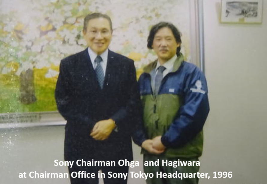
The chairman of Sony, Mr. Ohga and other Sony Executives were very happy
about the happy result of the Patent War.
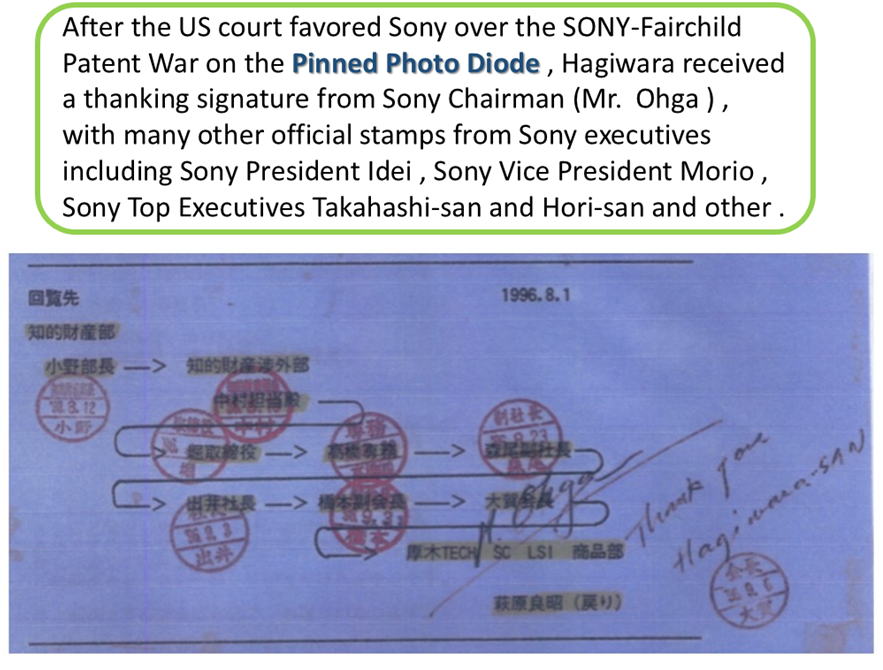
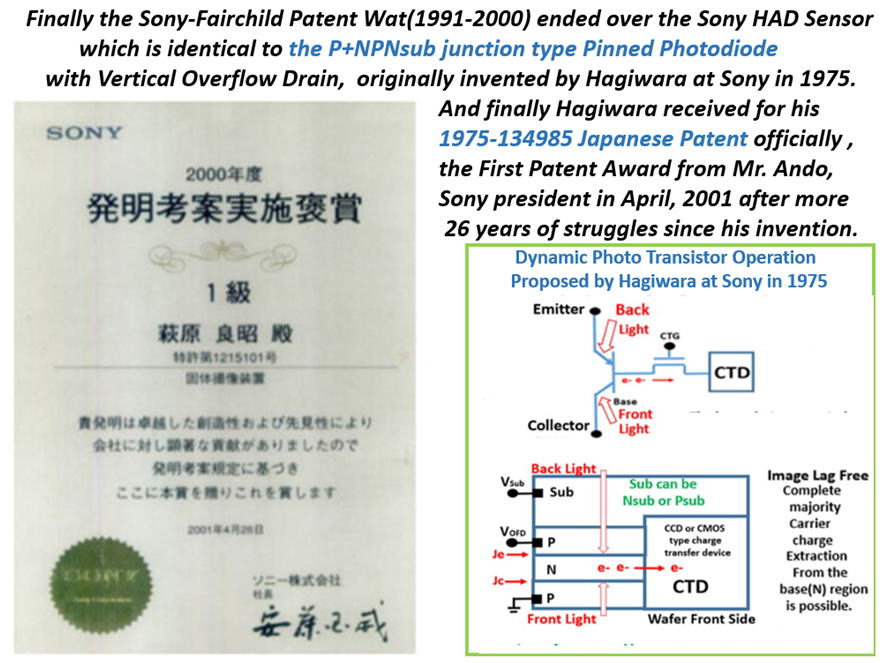
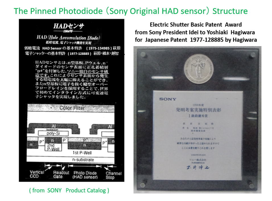
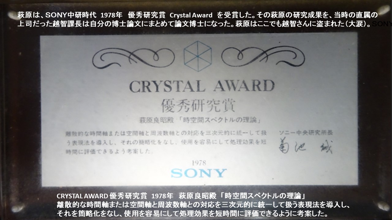
Hagiwara also received the Sony Central Research Center Crystal Award in 1978
for his image sensor time and space spectrum analysis.
Sony_acknowledged_that_Hagiwara_invented_PPD_with_VOD_for_Electric_Shutter_Function
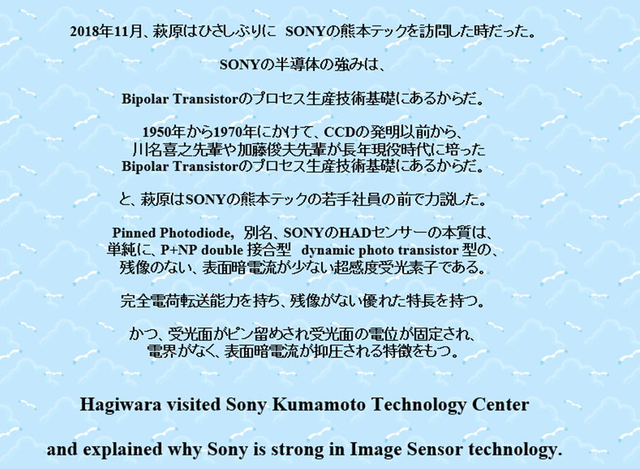
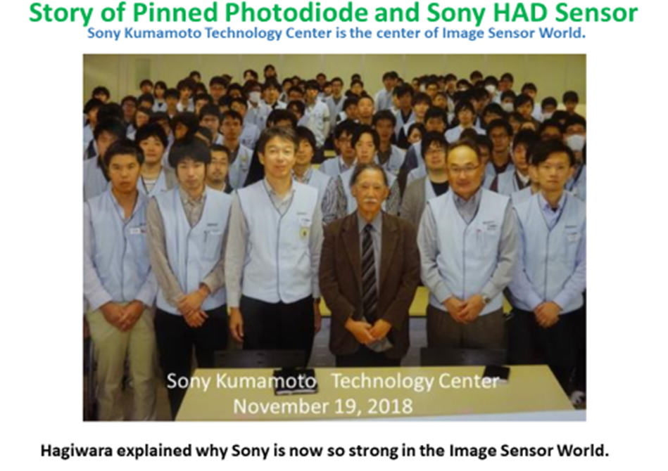
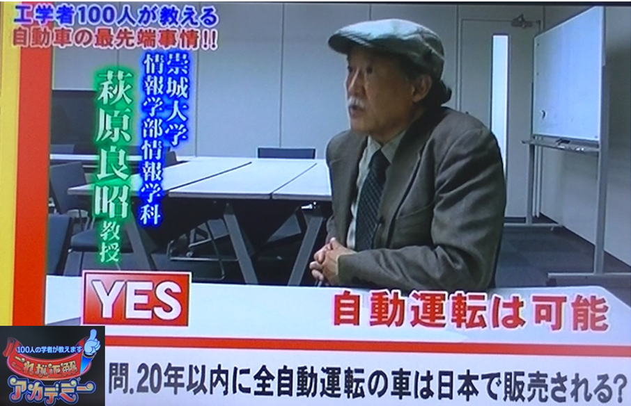
Prof. Yoshiaki Hagiwara at Sojo University was on TV .
The AIPS Self Driving Cars are on the way in near future.
*********************************************************************
Hagiwara_Japanese_Patents_and_Published_Papers_PDF_Files
*********************************************************************
1_Sony_vs_Loral_Patent_War_1_Reviews.pdf
1_Sony_vs_Loral_Patent_War_2_Supporting_Opinions.pdf
1_Sony_vs_Loral_Patent_War_3_E-mail_Communication_on_Sony_Loral_Patent_War_1996.pdf
1_Sony_vs_Loral_Patent_War_4_E-mail_communication_with_Albert_san_2018_07_10.pdf
1_Sony_vs_Loral_Patent_War_5_HAD_sensor_NEC_SONY_Patent_War.pdf
1_Sony_vs_Loral_Patent_War_6_JP1980_138026_NEC_Buried_Photodiode_Patent.pdf
1_Sony_vs_Loral_Patent_War_7_JP1978-1971_Toshiba_Yamada_VOD_patent.pdf
1_Sony_vs_Loral_Patent_War_53_pages.pdf
*********************************************************************
1_Sony_vs_Loral_PAtent_War_13_pages.pdf
2_The_evidence_that_Hagiwara_is_the_inventor_of_Pinned_Photodiode_7_pages.pdf
3_JP1975-127646_NPNP_triple_junction_Pinned_Photodiode_Patent_32_pages.pdf
4_JP1975-127647_NPN_double_junction_Pinned_Photodiode_Patent_22_pages.pdf
5_JP1975-134985_PNP_double_junction_Pinned_Photodiode_on_Nsub_Patent_7_pages.pdf
6_JP1977-126885_Elecric_Shutter_Clocking_Scheme_by_OFD_Punch_Thru_Action_13_pages.pdf
7_JP2014-135497_Digital_Transformation_Circuit_for_Image_Sensors_29_pages.pdf
8_JP2020_131313_on_Doubel_Junction_Pinned_Photodiode_Solar_Cell_65_Pages.pdf
9_P1978_Pinned_Photodiode_1978_Paper_by_Hagiwara_7_Pages.pdf
10_P1996_Pinned_Photodidoe_used_in_Sony_1980_FT_CCD_Image_Sensor_9_Pages.pdf
11_P2001_ESSCIRC2001_Micro-Electronics_for_Home_Entertainment_11_pages.pdf
12_P2008_ESSCIRC_2008_SOI_Design_in_Cell_Processor_and_Beyond_7_pages.pdf
13_P2013_ISSCC2013_Panel_Talk_25_pages.pdf
14_P2017_CoolChips_Panel_170419_29_pages.pdf
15_P2019_3DIC2019_Paper_on_3D_Pinned_Photodiode_6_pages.pdf
16_P2020_EDTM2020_PaperID_3C4_by_Hagiwara_4_pages.pdf
Hagiwara_Japanese_Patents_and_Published_Papers_302_pages.pdf
*********************************************************************
hagiwara-yoshiaki@aiplab.com for my activity at http://www.aiplab.com/
hagiwara@ssis.or.jp for my activity at http://www.ssis.or.jp/en/index.html
*********************************************************************