++++++++++++++++++++++++++++++++++++++++++++++
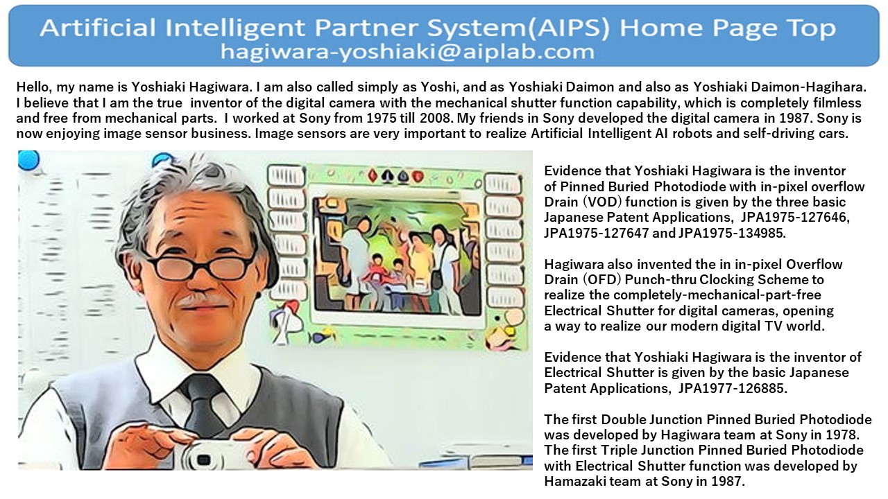
This is the Top Page of the AIPS HOMEPAGE
updated at 22:00 p.m. on Nov 30, 2021 ( Japan Time )
Please write me freely at hagwiara-yoshiaki@aiplab.com
++++++++++++++++++++++++++++++++++++++++++++++++++++++++
The Evidence that Yoshiaki Hagiwara at Sony Invented Pinned Photodiode in 1975.
++++++++++++++++++++++++++++++++++++++++++++++++++++++++
Dear Sir
Your honest, free and neutral opinion on the history of invention
and development efforts of image sensors is very important.
The truth should be revealed to all of the people in the world.
You are just one of them. But each one is very, very important.
I summarized my point of view on the history of the invention and the development efforts
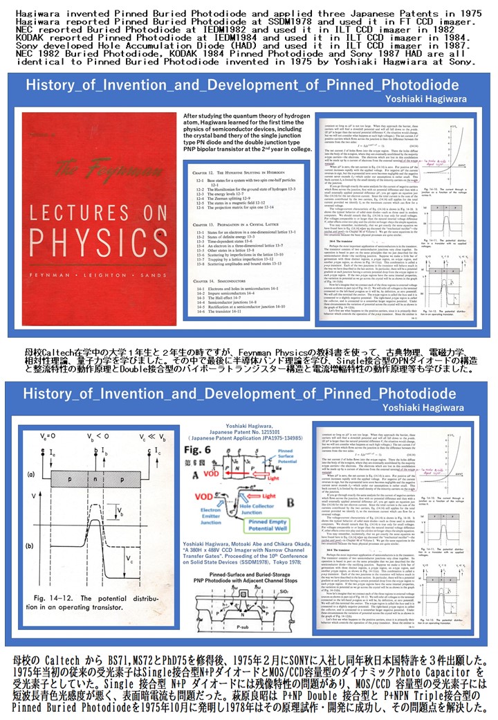
of Pinned Photodiode. When I jointed SONY in 1975 after receiving PhD from Caltech, Sony
people understood the importance of the CCD complete charge transfer operation and the
excellent feature of no image lag in the CCD/MOS dynamic photo capacitors. However
Sony was suffering the yield problem due to the strong surface electric field and the
poor short wave blue light sensitivity since the CCD/MOS dynamic photo capacitors have
the metallic polysilicon electrodes which do not pass the short wave blue light. As you may
know the short wave blue light cannot penetrate more than 0.1 micro meter in depth in
the silicon crystal. The double dynamic photo transistor and the triple junction photo
thyristor were the answers which do not have the surface electric field nor the metallic
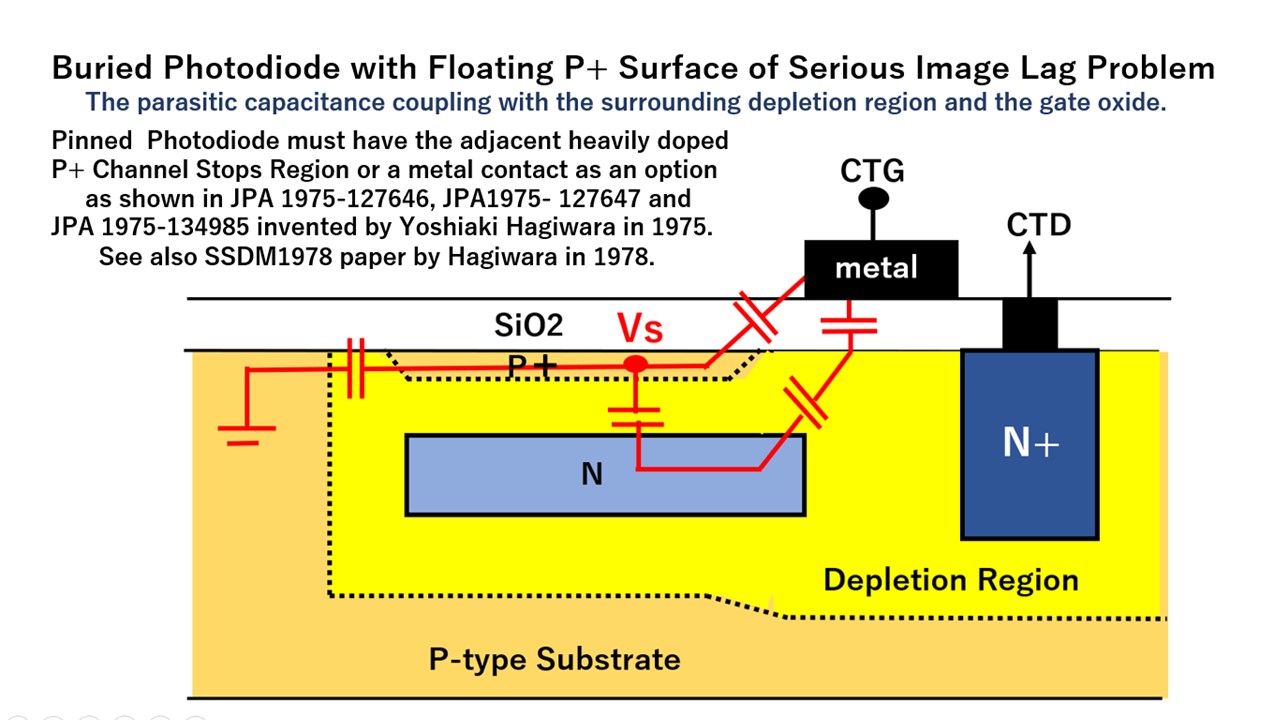
electrodes. I applied Japanese patents JP1975-127646, JP1975-127647 and JP1975-134985.
The proposed photodiodes were intended to be applied to the interline CCD image sensors
as explained in my Japanese 1975 patents . I developed the P+NP double junction type photodiode
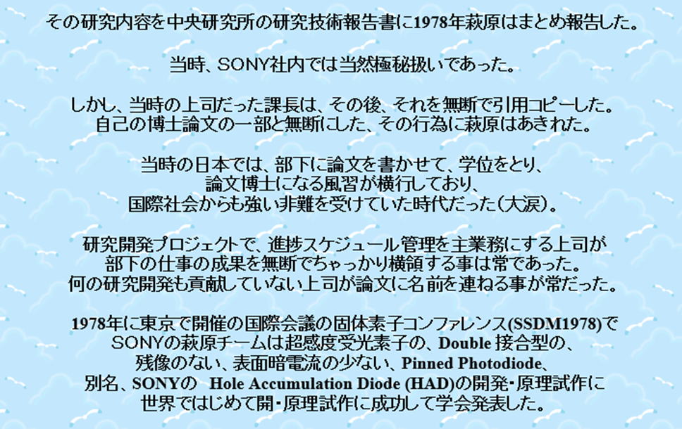
in 1978 used it in the FT CCD image sensors and reported at SSDM1978 conference in Tokyo.
After that , SONY kept silent since it was a top secrete project in SONY. SONY took more than
8 years to develop and make the passport size portable video cameras with the P+NPN triple
junction type photodiode with the in-pixel overflow drain with the complete electrical
shutter function for action pictures. Sony was only the maker who could produce the camera.
I summarized the details in the site shown below. The problem was that I forgot completely
myself the details of my 1975 inventions since I was busy since 1980 in developing the system
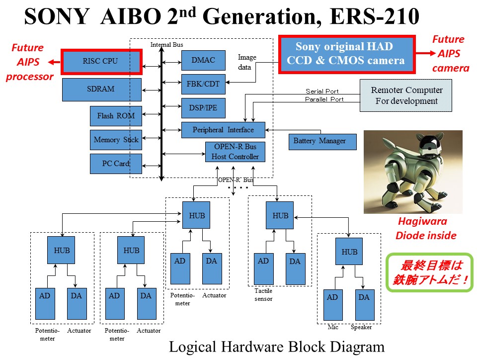
LSI chip sets such as for the SONY AIBO robots and the PS2 and PS3 Play Station Game Machines.
I uploaded here the complete form of my point of view on the PPD invention and development efforts.
I wish people would kindly read this for me and let me know what they think about this.
I am not asking your opinion on the patent issues. Patent issues
were already settled and no problems. Sony is now enjoying the
image sensor business being protected by Hagiwara 1975 Pinned
Photodiode patents. KODAK , NEC and Fairchild also did apply
similar PPD patents. But they were all applied later than 1975.
I am asking your opinion on who is the inventor and who
first developed Pinned Photodiode and reported in the
international technical conference.
These facts are important for the history of image sensors and
have very important meanings as back ground information
and for educational purpose for young generations who
may have interest in image sensors and its history.
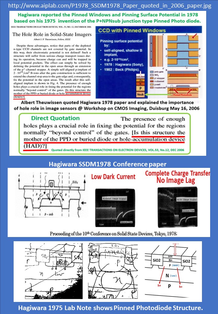
The SSDM1978 Conference held in Tokyo in 1978 is also an
international conference but with a very limited number.
The published SSDM1978 conference journal paper is not widely accessed.
But Albert Theuwissen found my SSDM1978 paper after 18 years
and quoted my original 1978 PPD work in his IEEE2006 paper.
Albert Theuwissen did not emphasize the complete charge transfer feature of
Pinned Photodiode since CCD has already the complete charge transfer feature.
The complete charge transfer feature was nothing new.
The importance of Pinned Photodiode were
(1) The excellent short wave blue sensitivity and
(2) the Low Surface Dark Current.
Firstly, since CCD has the metal electrode, it has a poor short wave
blue light sensitivity.
Secondly, the CCD/MOS dynamic photo capacitor has a strong surface electric field
which induces the undesired surface dark current.
However, Albert Theuwissen apparently and SONY( Hagiwara) already understood
the feature of the complete charge Transfer mode of Pinned Photodiode.
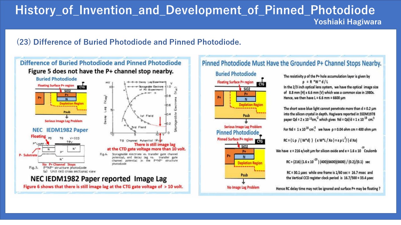
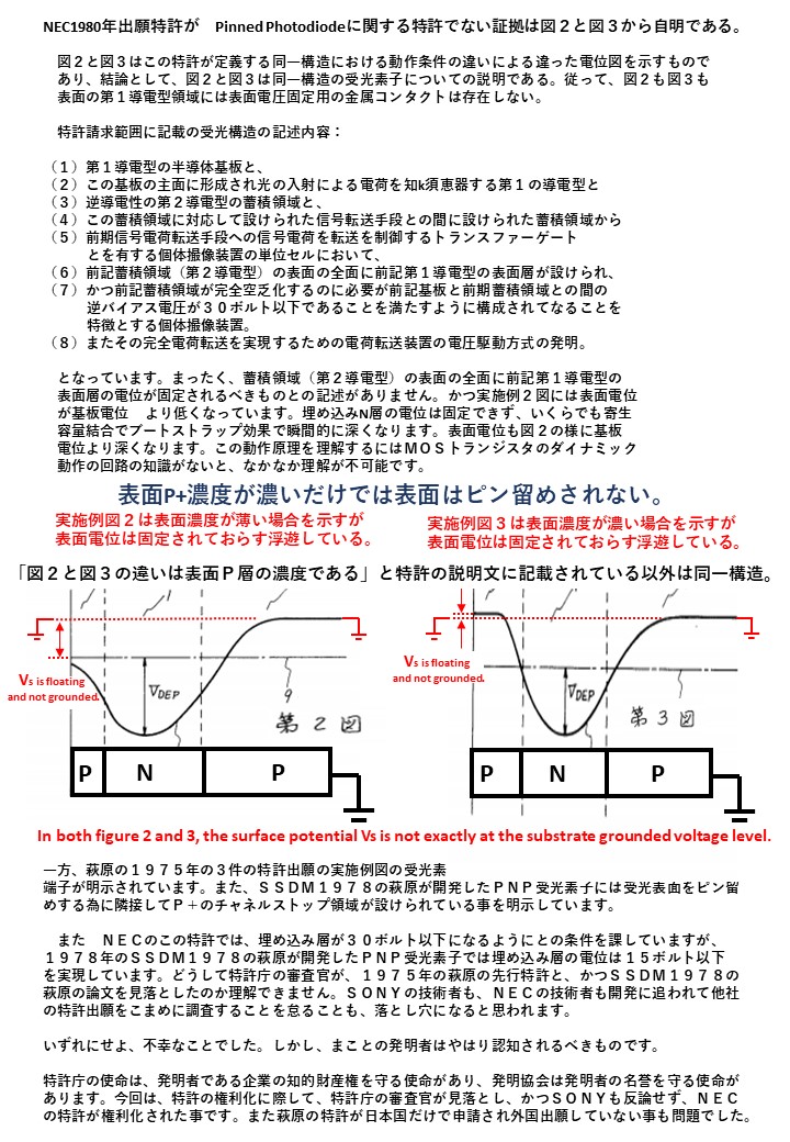
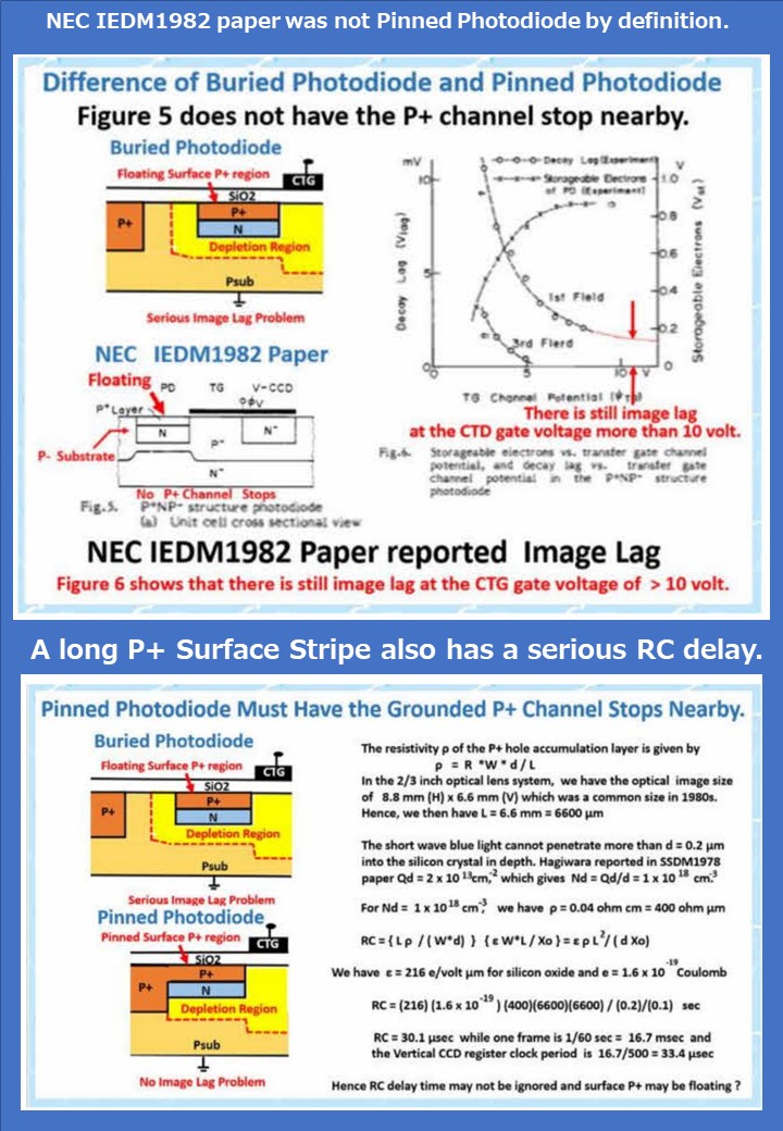
NEC IEDM1982 paper by Teranishi reported the importance of the image lag feature
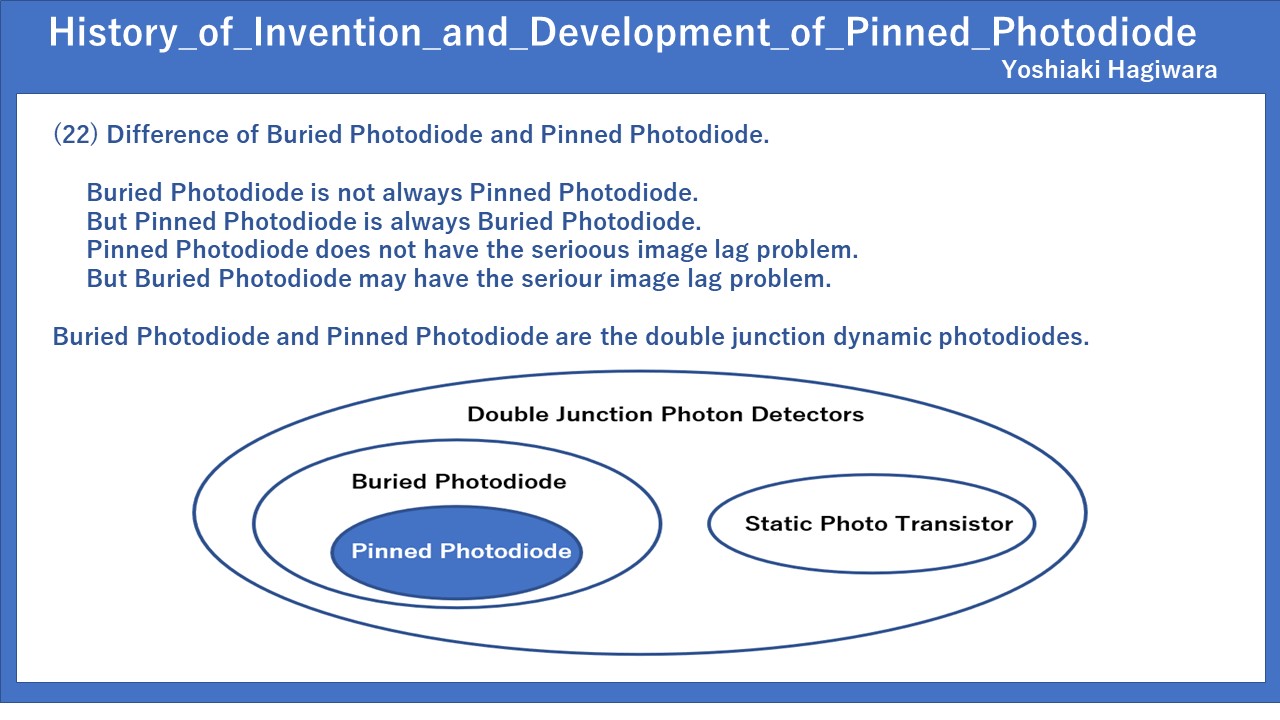
of Buried Photodiode. But Buried Photodiode is not always Pinned Photodiode.
NEC IEDM1982 paper by Teranishi also reported the serious undesired image lag
feature of the NEC1982 Buried Photodiode in the IEDM1982 paper. Any photodiode
with image lag feature is not Pinned Photodiode according to the Fossum Paper.
Hence NEC IEDM1982 paper was not Pinned Photodiode by definition.
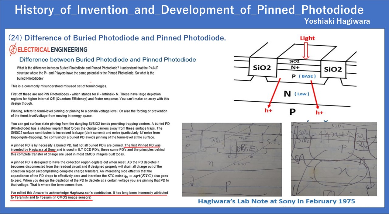
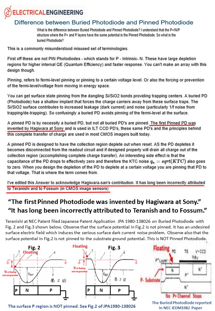
The Difference of Pinned Photodiode and Buried Photodiode was well explained in
the article which says ,"...acknowledge Hagiwara-san's contribution.It has long
been incorrectly attributed to Teranishi and to Fossum (in CMOS image sensors)"
"A pinned PD is designed to have the collection region deplete out when reset.
AS the PD depletes it becomes disconnected from the readout circuit and
if designed properly will drain all charge out of the collection region
(accomplishing complete charge transfer). An interesting side effect is
that the capacitance of the PD drops to effectively zero and therefore
the KTC noise qn=sqrt(KTC) also goes to zero. When you design the depletion
of the PD to deplete at a certain voltage you are pinning that PD to that
voltage. That is where the term comes from. I've edited this Answer to
acknowledge Hagiwara-san's contribution. It has long been incorrectly
attributed to Teranishi and to Fossum (in CMOS image sensors)"
Actually the in-pixel active sensor was first invented and reported
in 1968 by Peter Noble at Plessy in England UK before Fossum work in 1990.
These truth was not well understood widely.
Teranishi and Fossum are well received to the world for their contributions.
But they never quoted Hagiwara and Noble previous old works.
The people misunderstood that Teranishi and Fossum were
the first inventors and the first developers.
Patent issues are settled and now Sony enjoy the image
Sensor business with advantage over KODAK, NEC ,
Fairchild and other competing companies. Sony has
Hole Accumulation Diode (HAD) which is identical to
Pinned Photodiode in the world wide business with
more than 60 to 70 % share of image sensor devices.
Now the KODAK-named Pinned Photodiode reported in IEDM1984
is now considered as the invention by Teranishi at NEC in 1980,
according to the paper "A Review of the Pinned Photodiode
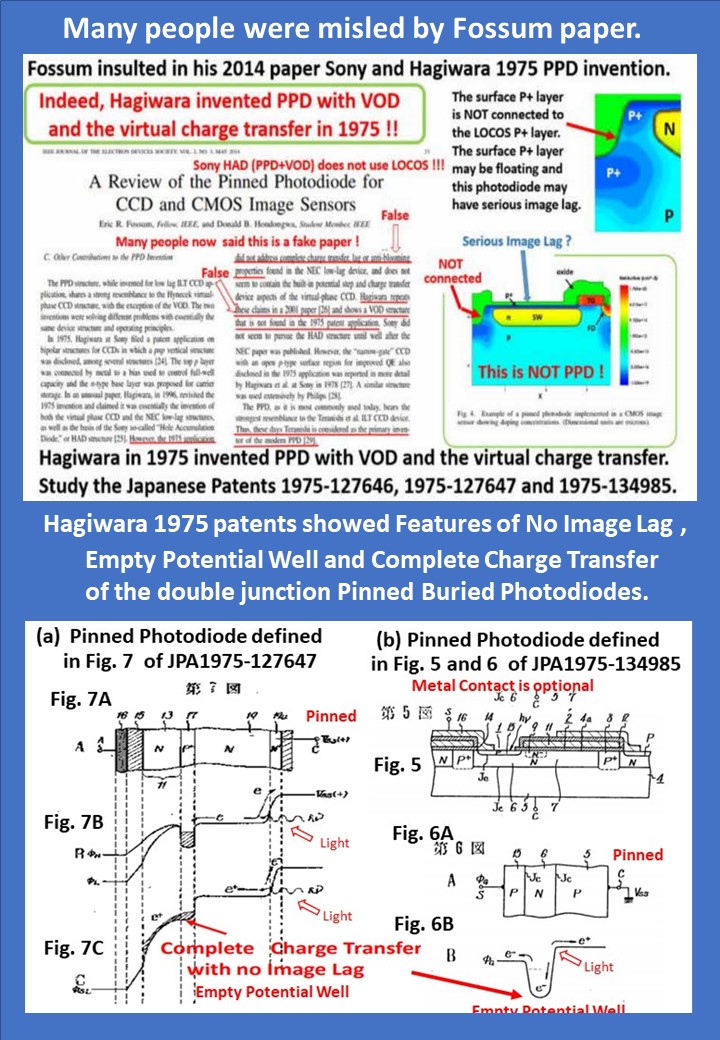
for CCD and CMOS Image Sensors" by E.Fossum. This Fossum
paper was attacking Hagiwara 1975 patent and SSDM1978
paper with misleading descriptions on no image lag issue.
Hagiwara 1975 patent and SSDM1978 paper did report the
complete charge transfer operation and showed the empty
potential well profile which are signs of no image lag feature.
The truth is that Hagiwara proposed 1975 the now-called
Pinned Photodiode in form of the double PNP and triple PNPN
junction dynamic photodiodes originally.
The double PNP and triple PNPN junction dynamic photodiodes
in 1975 and reported the double PNP junction dynamic
photodiode in Hagiwara SSDM1978 paper.
The patent issues were settled and no problems.
In the secret patent disputes and the public US courts ,
Fairchild, KODAK, NEC in the past attacked Sony on the
basic Pinned Photodiode patents but they were all not
successful. NEC gave up image sensor business and
Fairchild and KODAK made friendly technical agreements
with Sony now. I am not asking about the patent issue.
I need to hear your personal opinion on the historical background
of the invention and the Innovation efforts of Pinned Photodiode.
The truth should be revealed to all of the people in the world.
You are just one of them. But each one is very, very important to me.
Fossum paper claims that Hagiwara JPA1975-134984 and
Hagiwara 1978 paper did not describe the image lag feature.
I believe Fossum misunderstood my 1975 patent and 1978 paper.
Hagiwara JPA1975-134984 showed an empty potential of
the buried N storage region of the double junction PNP
dynamic photo transistor structure with the emitter and
the collector terminals both pinned, which is identical to
Pinned Photodiode. As you know the empty potential well
implies the complete charge transfer operation which results
in the excellent feature of no image lag in video camera.
Hagiwara SSDM1978 paper reported the output wave forms of
the image sensor using the double PNP junction photodiode
with the pinned P+ surface region directly connected to
the adjacent P+ channel stops, which is also identical to
the definition of Pinned Photodiode. The output wave forms
showed a very low total surface dark current of less than 3%
and the complete charge transfer efficiency of more than 99.995%
which implies the excellent feature of no image lag.
My work was cited in "A Review of the Pinned Photodiode for CCD
and CMOS Image Sensors" by E.Fossum. Actually E.Fossum was
attacking my 1975 PPD patent and SSDM1978 PPD paper.
Please kindly read carefully Fossum paper. Fossum was not telling
the truth about Hagiwara 1975-134985 patent and Hagiwara
SSDM 1978 paper. Fossum paper was misleading and had a wrong
conclusion.
I have reported the image lag feature of the complete charge
transfer operation both in my 1975 PPD patent and SSDM1978
PPD paper. Fossum did not read carefully or does not understand
the details of my 1975 PPD patent and SSDM1978 PPD paper.
The truth should be revealed to all of the people in the world.
You are just one of them. But each one is very, very important to me.
I would like to hear your personal opinion on this.
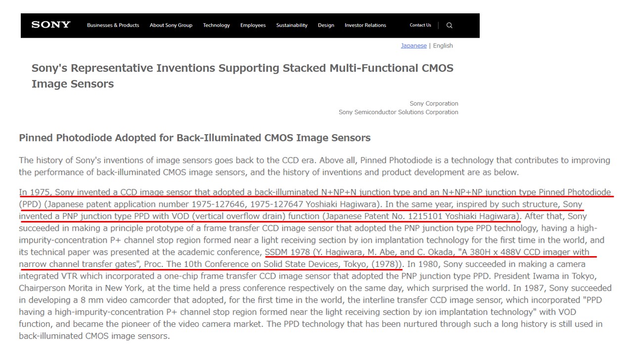
For your information, Sony wrote an article
regarding the original invention of Pinned Photodiode
in the Sony Official Homepage:
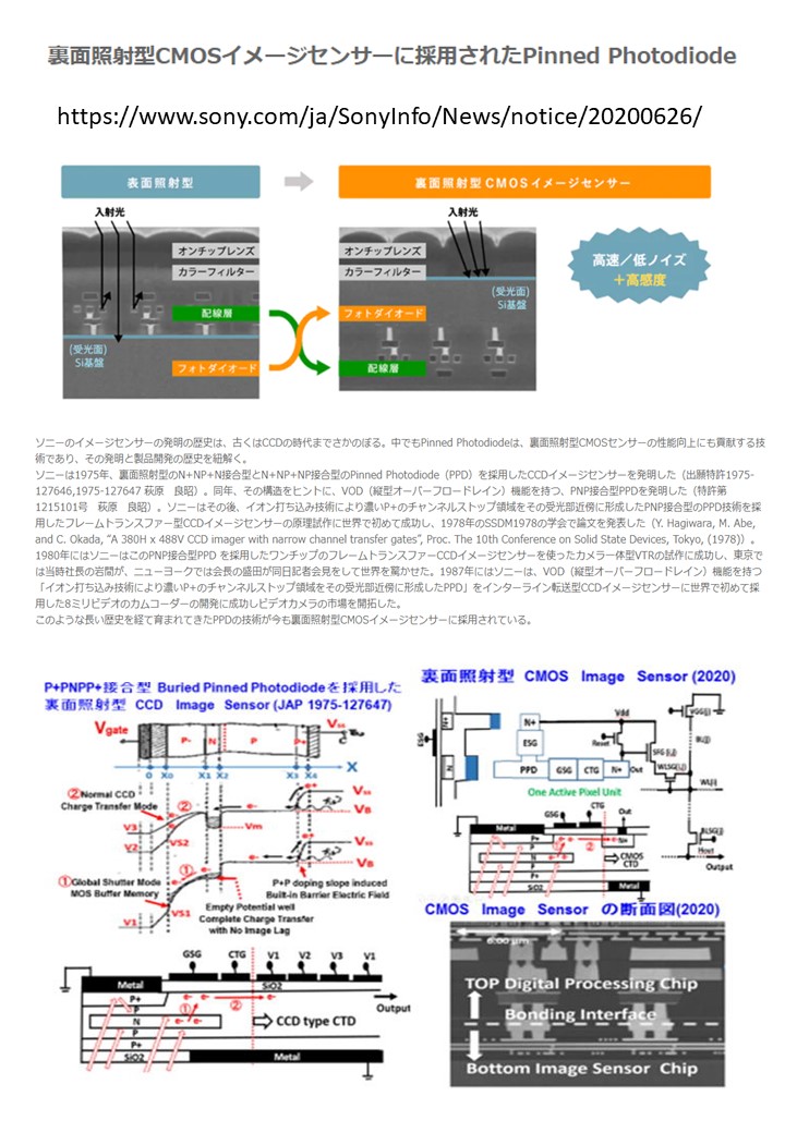
"In 1975, Sony invented a CCD image sensor that adopted a back-illuminated N+NP+N junction type
and an N+NP+NP junction type Pinned Photodiode (PPD) (Japanese patent application number
1975-127646, 1975-127647 Yoshiaki Hagiwara). In the same year, inspired by such structure,
Sony invented a PNP junction type PPD with VOD (vertical overflow drain) function (Japanese
Patent No. 1215101 Yoshiaki Hagiwara). After that, Sony succeeded in making a principle prototype
of a frame transfer CCD image sensor that adopted the PNP junction type PPD technology, having a
high-impurity-concentration P+ channel stop region formed near a light receiving section by ion
implantation technology for the first time in the world, and its technical paper was presented
at the academic conference, SSDM 1978 (Y. Hagiwara, M. Abe, and C. Okada, "A 380H x 488V CCD
imager with narrow channel transfer gates", Proc. The 10th Conference on Solid State Devices,
Tokyo, (1978)). In 1980, Sony succeeded in making a camera integrated VTR which incorporated
a one-chip frame transfer CCD image sensor that adopted the PNP junction type PPD. President
Iwama in Tokyo, Chairperson Morita in New York, at the time held a press conference respectively
on the same day, which surprised the world. In 1987, Sony succeeded in developing a 8 mm video
camcorder that adopted, for the first time in the world, the interline transfer CCD image sensor,
which incorporated "PPD having a high-impurity-concentration P+ channel stop region formed near
the light receiving section by ion implantation technology" with VOD function, and became the
pioneer of the video camera market. The PPD technology that has been nurtured through such a
long history is still used in back-illuminated CMOS image sensors."
The Society of Semiconductor Industry Specialists (SSIS) of Japan
Society of Semiconductor Industry Specialists (ssis.or.jp)
also wrote an article regarding the original invention of Pinned Photodiode
on the SSIS official Homepage:
The Society of Semiconductor Industry Specialists (SSIS) of Japan explained
and claimed in details as
"The Pinned Photodiode is a photodiode in which the entire N layer is
covered with a P layer. The part of the P layer on the light incident
surface is heavily doped P+. Kodak named this structure Pinned Photodiode
in 1984 because the P+ surface of the light incident surface was pinned
to the substrate potential.
This device has features such as high light sensitivity, wide dynamic range,
image lag free, much smaller dark current due to reduced influence of GR center
on the light receiving surface, and no white scars.
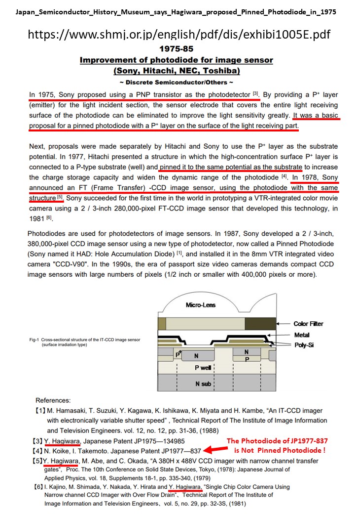
In 1975, Sony proposed using a PNP transistor as the photodetector [3].
By providing a P+ layer (emitter) for the light incident section,
the sensor electrode that covers the entire light receiving surface of
the photodiode can be eliminated to improve the light sensitivity greatly.
It was a basic proposal for a pinned photodiode with a P+ layer on the surface
of the light receiving part."
The reference [3] is my original Japanese Patent on Pinned Photodiode.
The photodiode structure was originally defined as the double PNP dynamic photo transistor
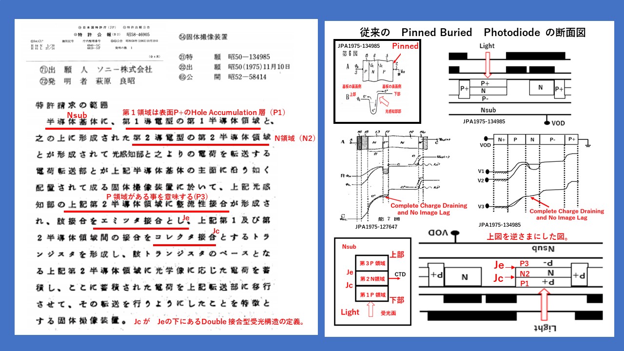
and the triple junction PNPN dynamic photo thyristor in my patent application Jp1975-134985.
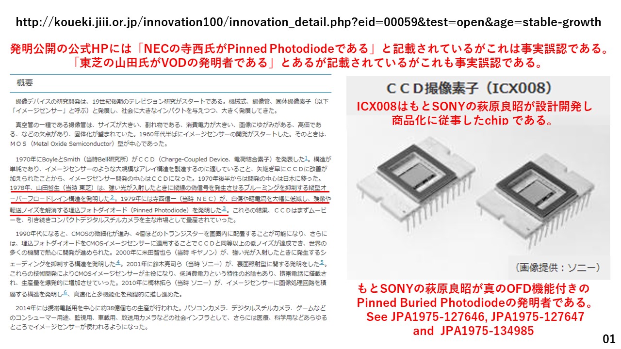
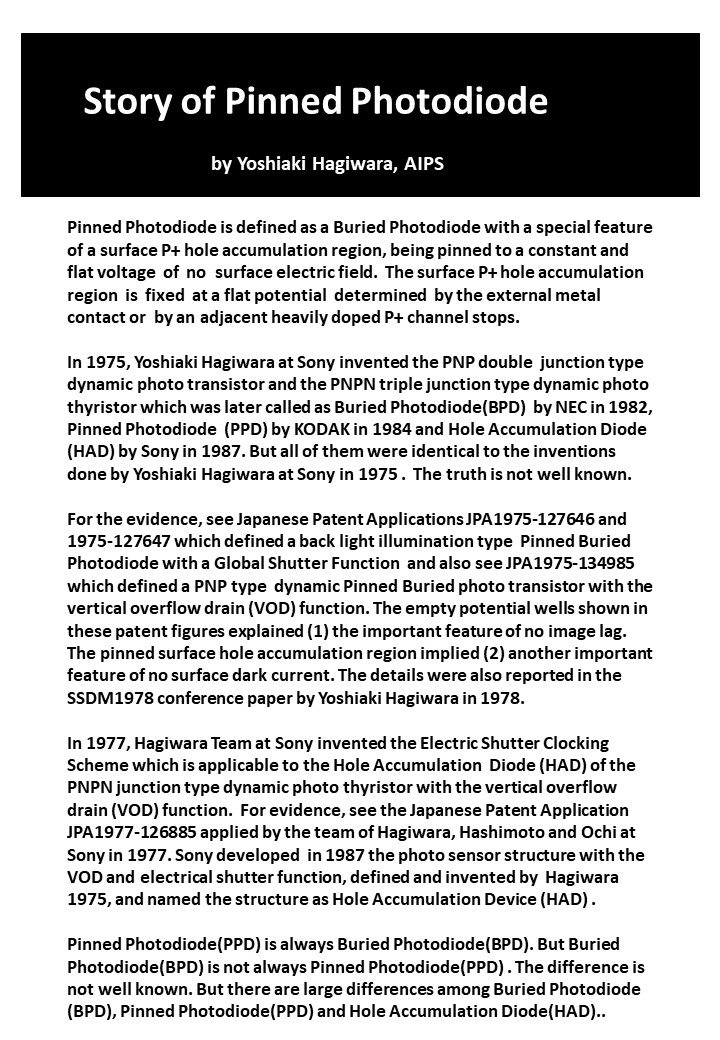
The structure was later called as Buried Photodiode by NEC in 1982, Pinned Photodiode by KODAK in 1984,
and as the Hole Accumulation Diode (HAD) by Sony in 1987.
But all of them are identical to my 1975 invention.
I believe I am the inventor of Pinned Photodiode in 1975 and developed Pinned Photodiode in 1978.
And Sony built the video movie camera used Pinned Photodiode
in the one chip NTSC full size Frame Transfer CCD image sensor in 1980
The details of my works are explained in the following publications.
Would you kindly read my papers and let me know your personal opinion on
who really invented Pinned Photodiode and developed it for the first time in the world ?
++++++++++++++++++++++++++++++++++++++++++++++++++++++++
Paper Accepted with a minor revision. Reviews' Comments:
++++++++++++++++++++++++++++++++++++++++++++++++++++++++
"This is a comprehensive paper, well designed, performed and written.
The logicality of this paper is quite good and the main body provides
sufficient information. The study abstract is concise and clearly presented,
and the figures in the article have well illustrated the study. Meanwhile,
the author gives a comprehensive description in conclusion.
This is a very instructive research. It is suggested that recommendations
for follow-up or future work on this topic should be made."
+++++++++++++++++++++++++++++++++++++++++++++++++++++++++
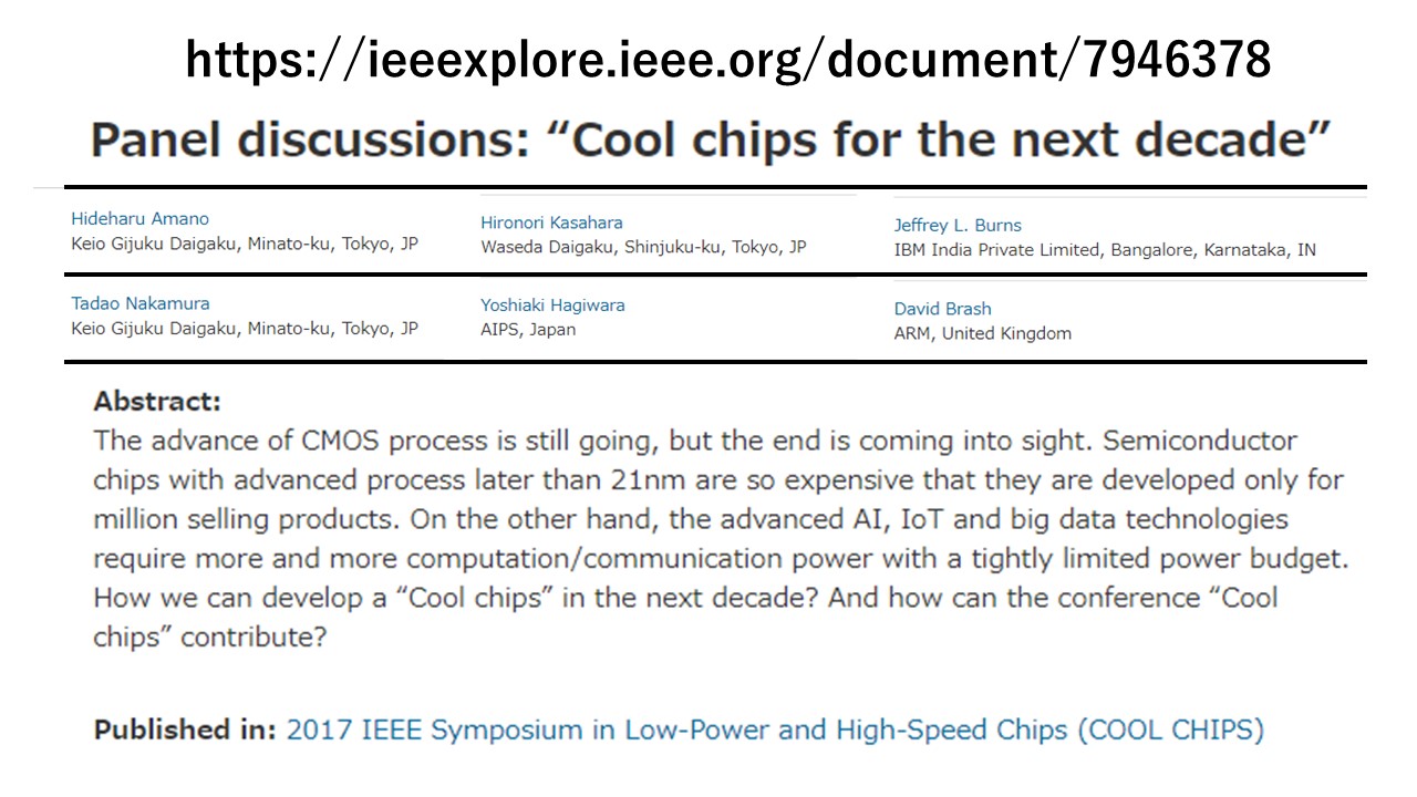
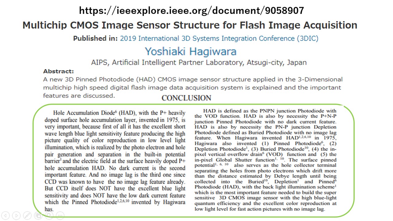
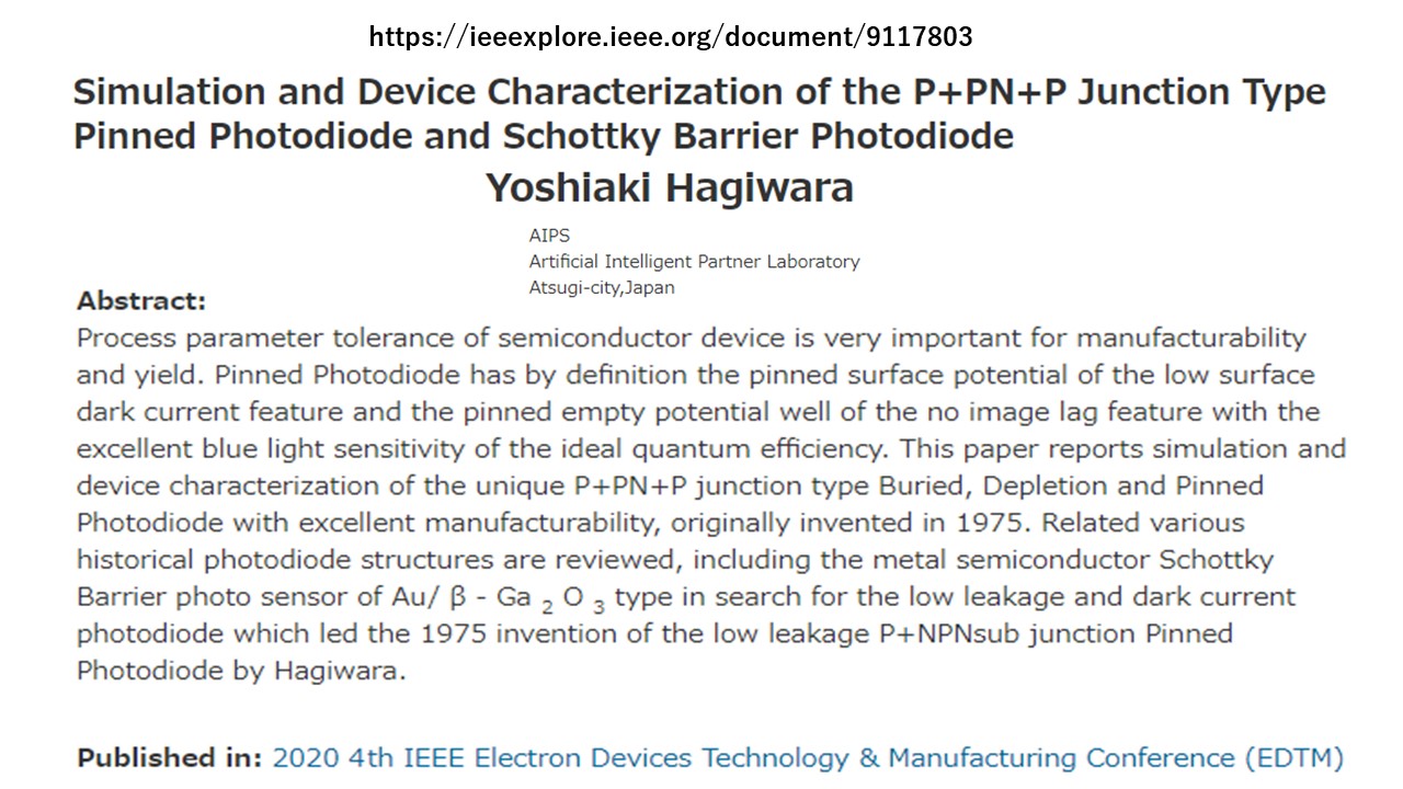
List of Related Published Papers on Pinned Photodiode
+++++++++++++++++++++++++++++++++++++++++++++++++++++++++
Unfortunately these Japanese Patent Applications of mine shown below were
written only in Japanese language and were never disclosed in details to
the English Speaking Community.
*********************************************************************
hagiwara-yoshiaki@aiplab.com for my activity at http://www.aiplab.com/
hagiwara@ssis.or.jp for my activity at http://www.ssis.or.jp/en/index.html
*********************************************************************
++++++++++++++++++++++++++++++++++++++++++++++++++++
On Nov 13, 2021, a Japanese Newspaper by Sangyou Times
wrote an aticle introducing Hagiwara.
++++++++++++++++++++++++++++++++++++++++++++++++++++
Yoshiaki Hagiwara wrote a book on
"the World of Artificial Intelligent Digital Circuits",
which is important and needed to built
the intelligent image sensor systems.
ISBM978-4-88359-339-2
Hard Cover, 460 page,
\ 9000 Japanese Yen + tax
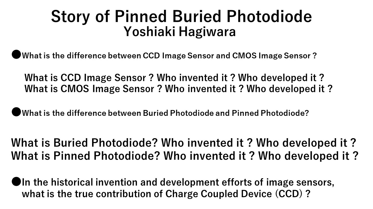
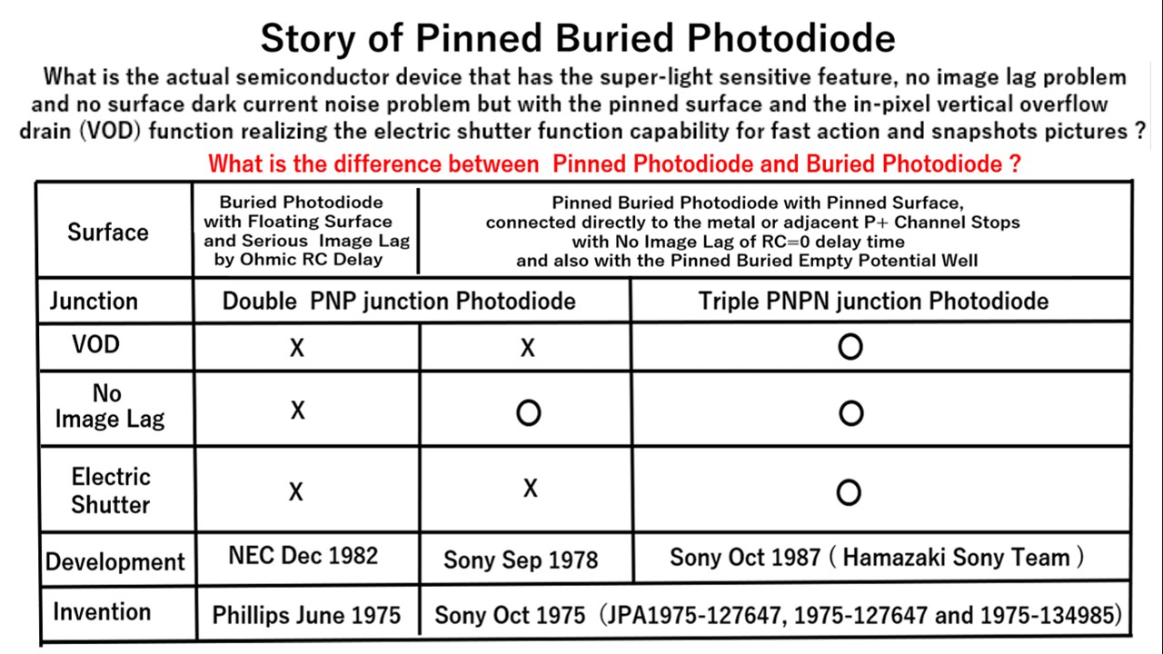
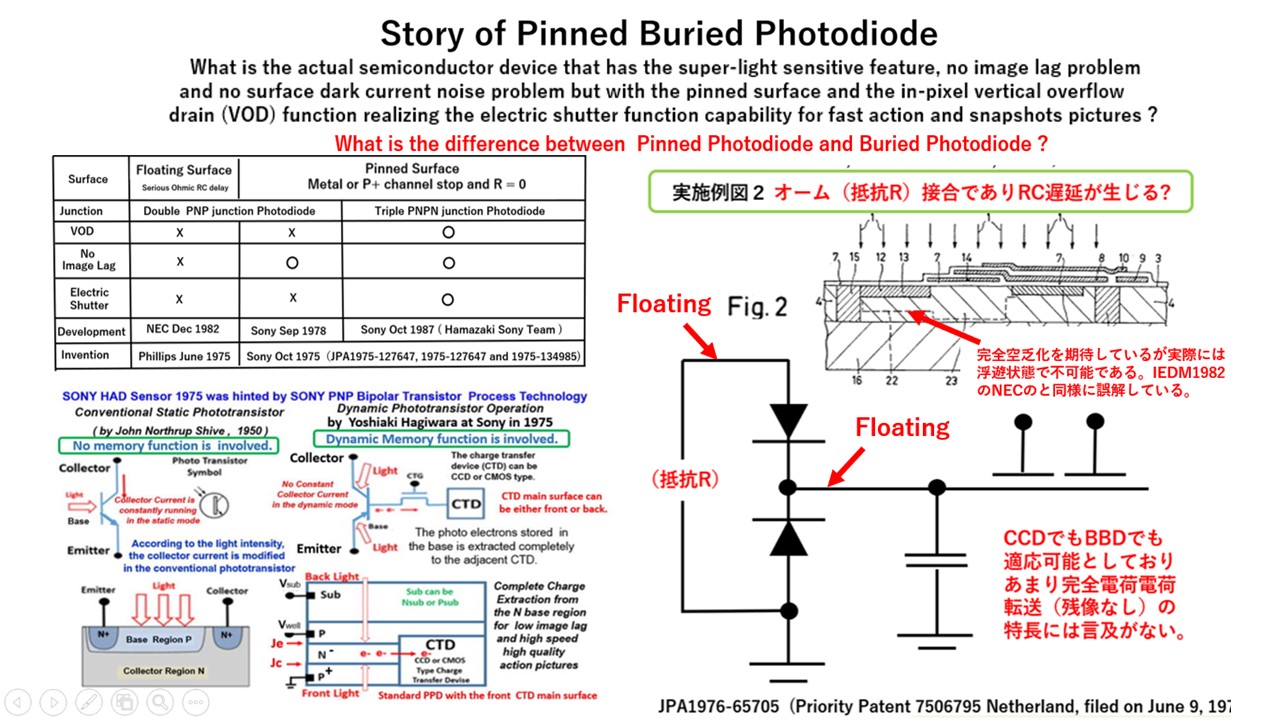
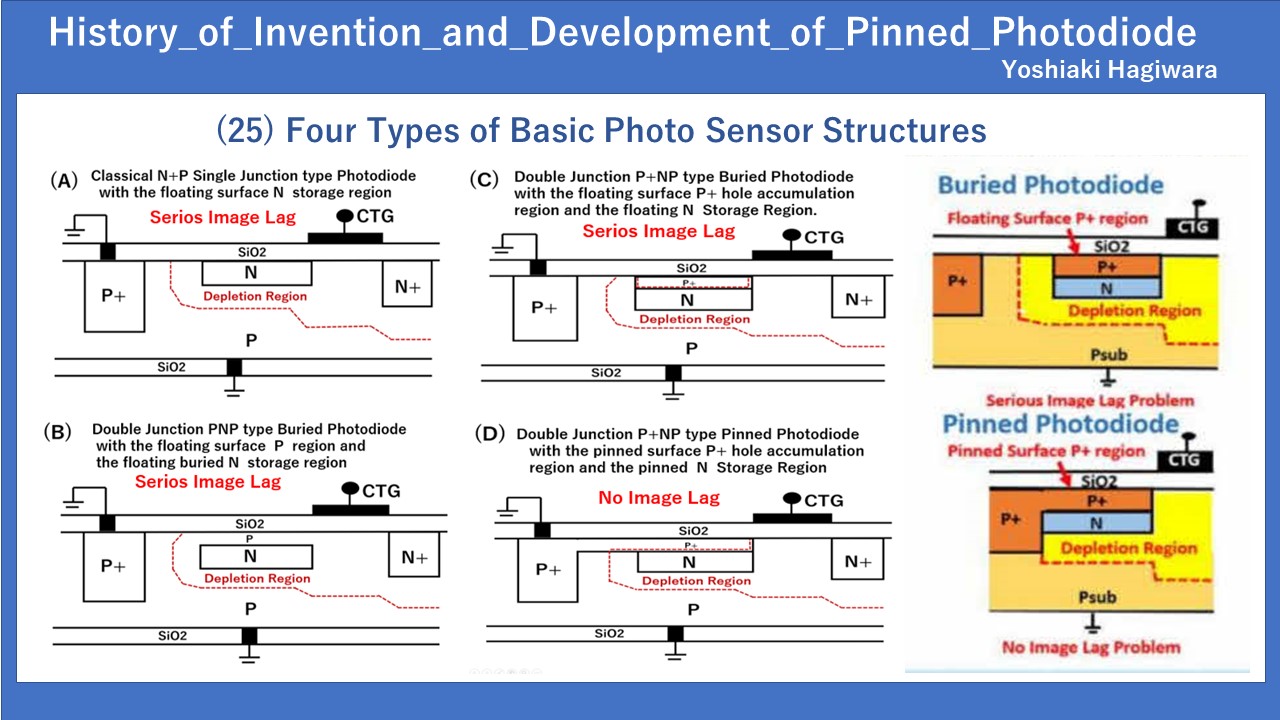
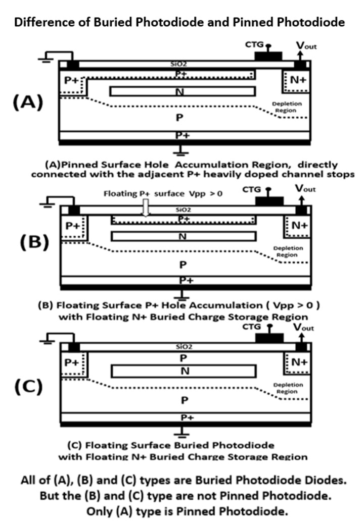
However, Buried Photodiode(BPD) is not always Pinned Photodiode (PPD).
Buried Photodiode(BPD) may not have the Pinned surface p region.
Buried Photodiode(BPD) may have the serious image lag problem.
Buried Photodiode(BPD) may have the serious surface dark curent
when the surface is completely depleted and has the surface strong electric field
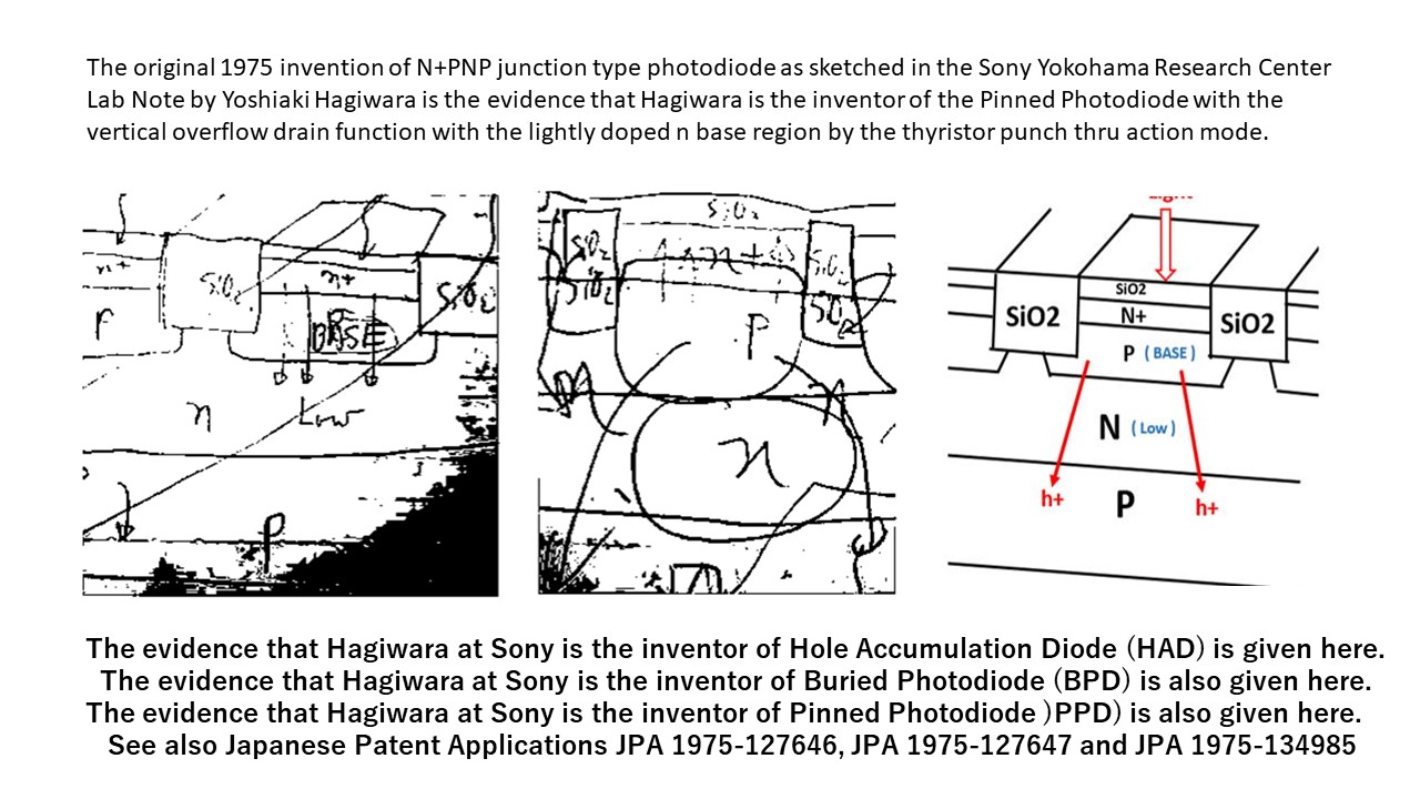
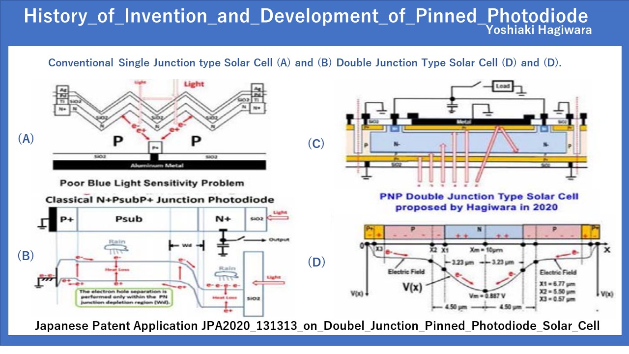
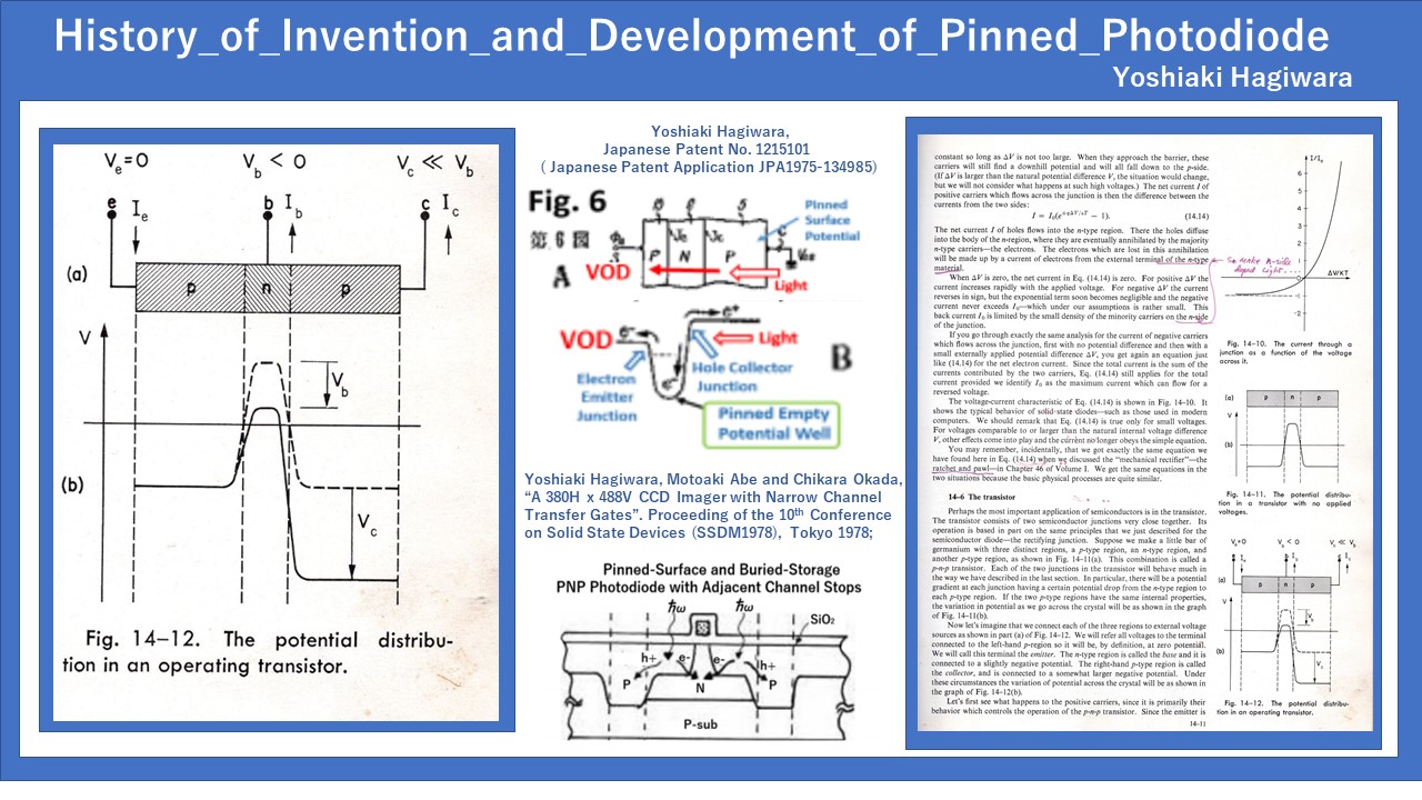
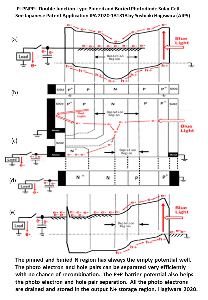
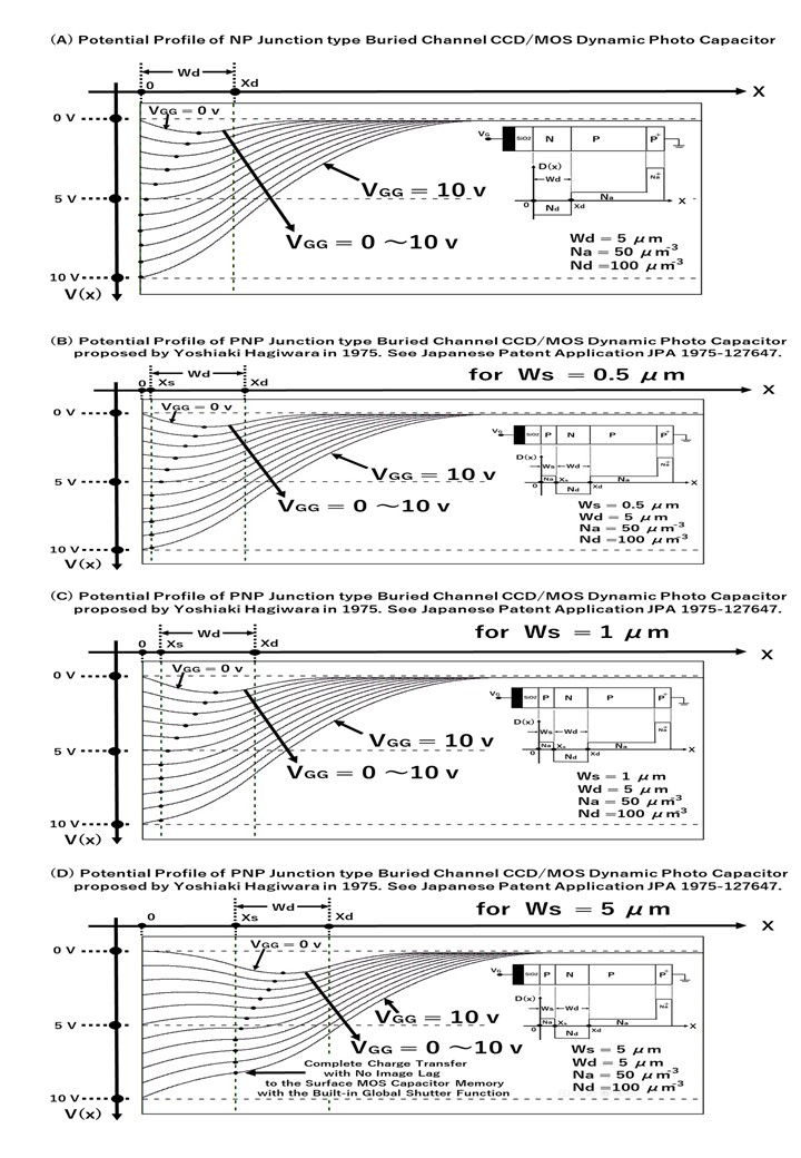
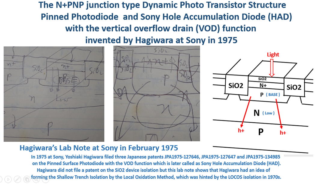
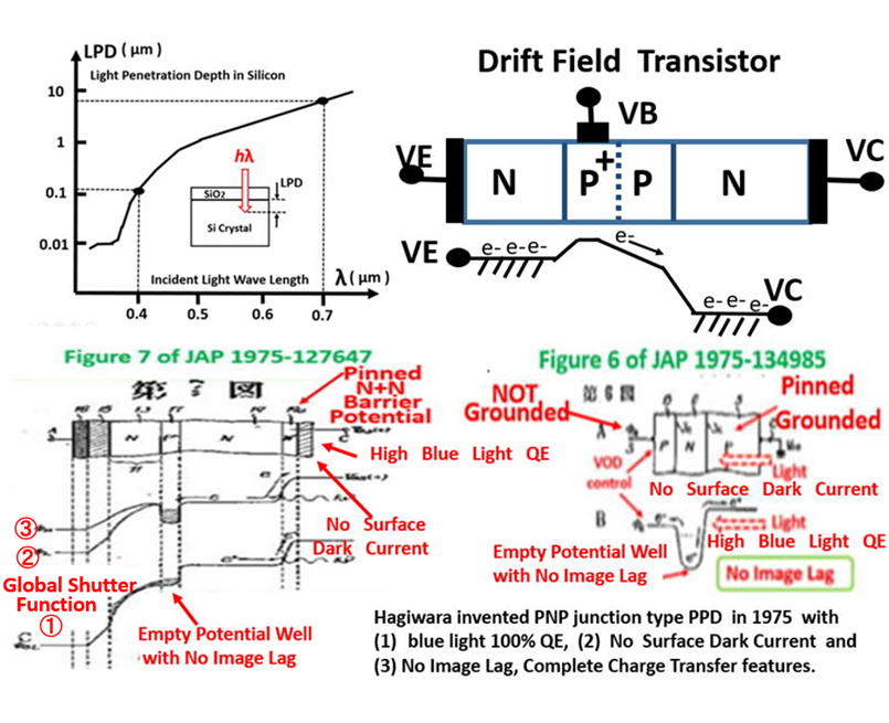
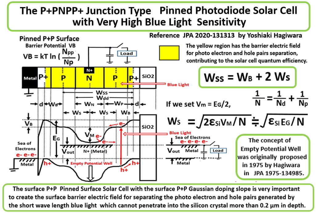
Pinned Photodiode (PPD) was also invented by Yoshiaki Hagiwara at Sony in 1975
in JPA 1975-127646 as a double junction type N+N-P+NP-P Buried Photodiode
and in JPA 1975-127647 as a triple junction type N+N-P+N Buried Photodiode
with the Pinned Surface N+N barrier electric field in the surface electron accumulation region
of the excellent short wave blue light sensitivity,
the very low surface dark current noise, and
the complete charge transfer capability of no image lag feature.
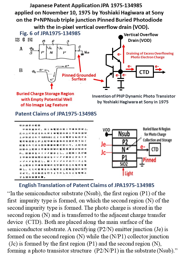
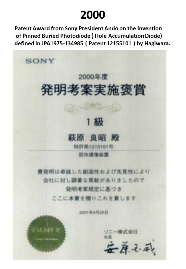
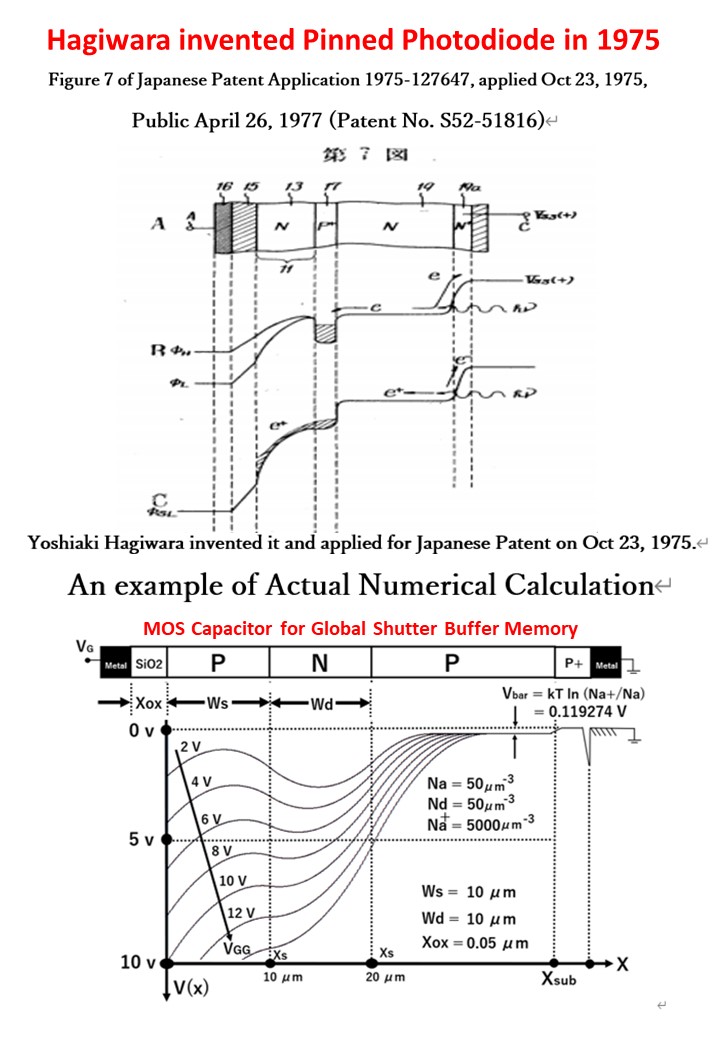
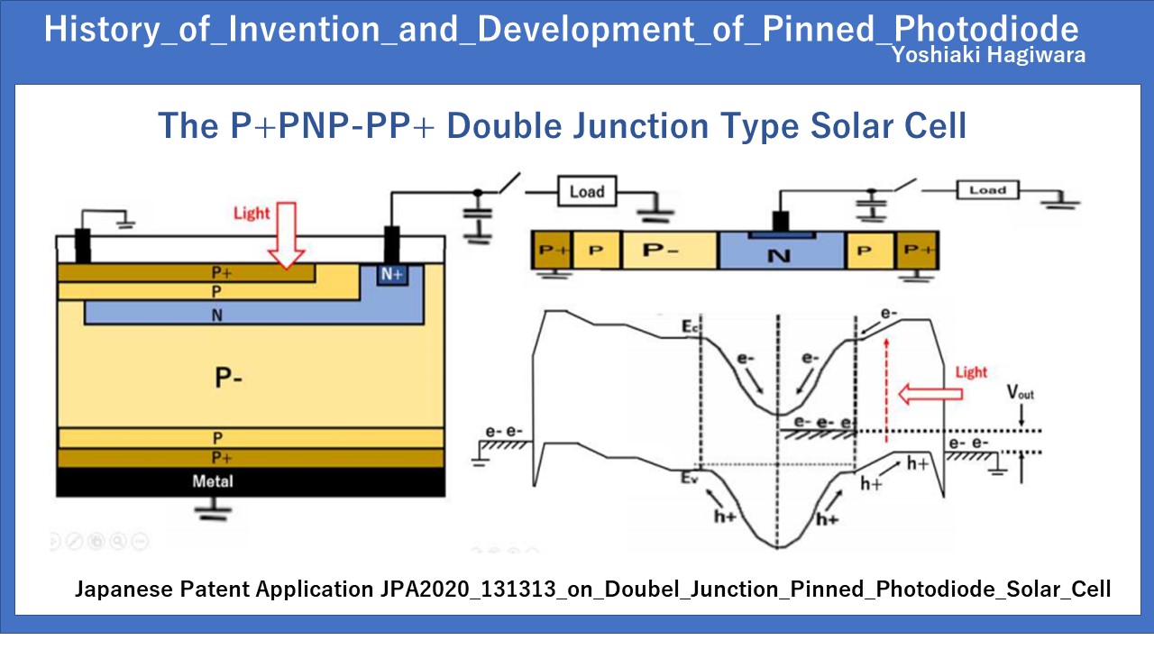
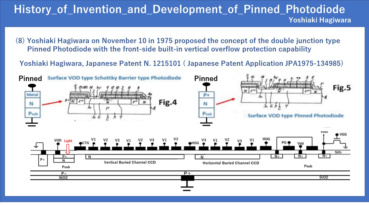
A triple junction type P+NPNsub Pinned Photodiode,
which is a double junction type P+NP Pinned Photodiode in the N type Silicon substrate Nsub,
was also invented in JPA 1975-134985 by Yoshiaki Hagiwara at Sony in 1975
with the built-in vertical overflow drain (VOD) capability.
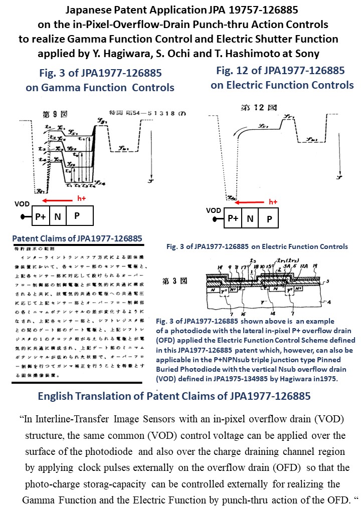
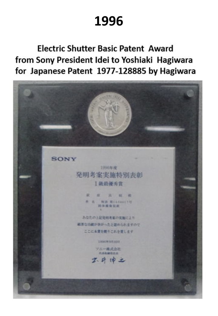
Electrical Shutter Function Clocking Scheme
of controling the punch thru voltage of the built-in verical overflow drain (VOD)
was also invented in JPA 1975-126885 by Yoshiaki Hagiwara at Sony in 1977
and was applied in the triple junction type P+NPNsub Pinned Photodiode
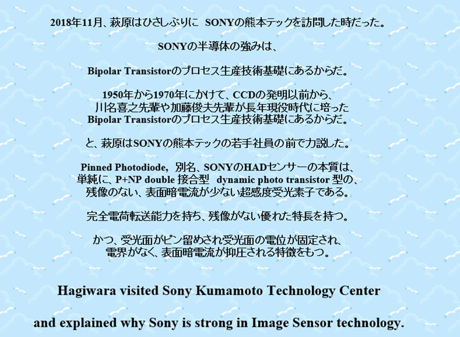
which was named in 1987 as Hole Accumulation Diode(HAD) by Sony Hamazaki Team .
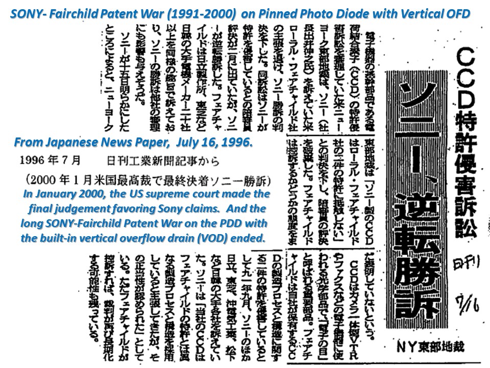
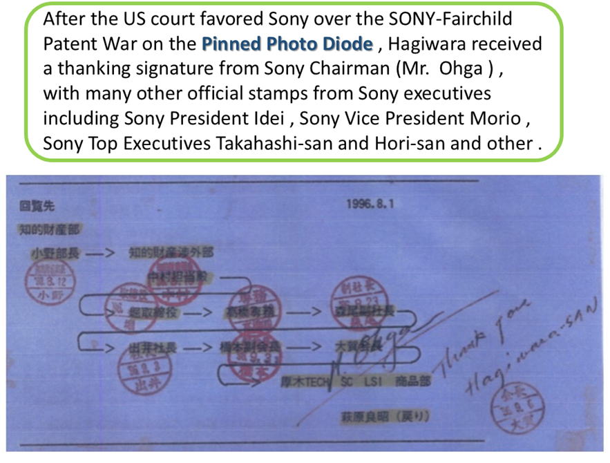
Hagiwara had to defend his 1975 Pinned Photodiode Basic Patents
JPA 1975-127646, JPA 1975-127647 and JPA 1975-134985
from Faircild, NEC and Kodack Patent Attacks
more than 15 years from 1990 till 2015.
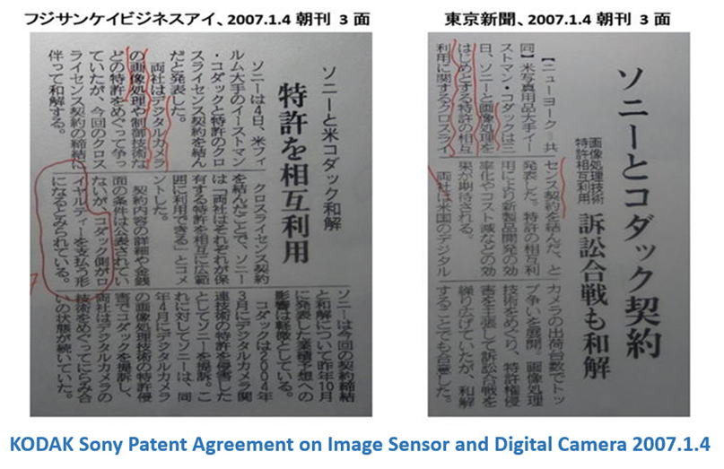
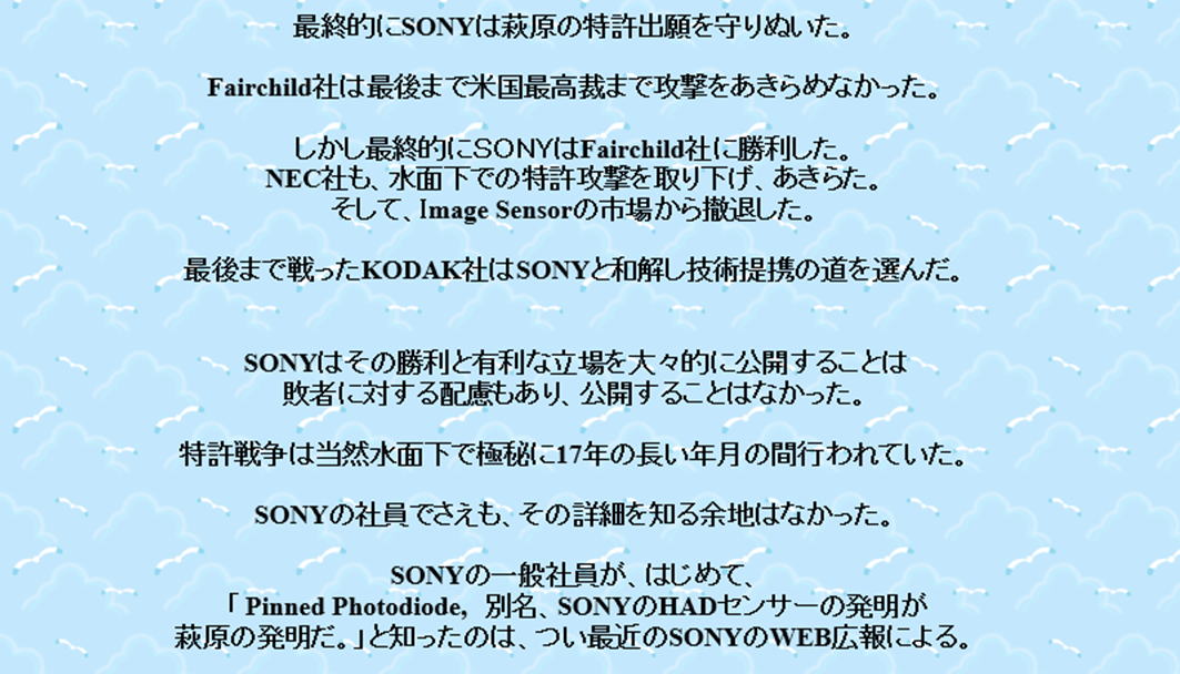
Sony won the Farichi/Sony Patent War in 2000.
NEC gave up patent disputes and stopped image sesnor business.
Sony and Kodak made a friendly technical cross liscence mutual agreement.
--P036--
Sony and Kodak made a friendly technical cross liscence mutual agreement
while NEC gave up patent disputes and stopped image sesnor business..
--P037--
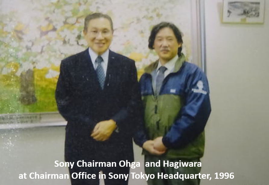
The chairman of Sony, Mr. Ohga and other Sony Executives were very happy
about the happy result of the Patent War.
--P038--
--P039--
--P040A--
--P040B--
--P040C--
--P040D--
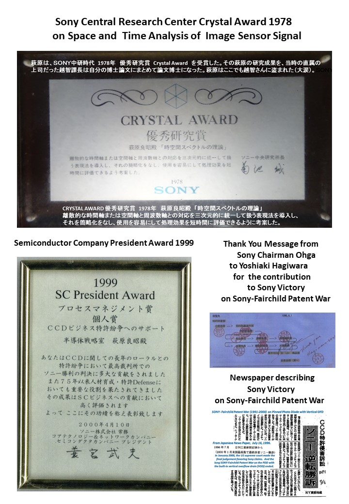
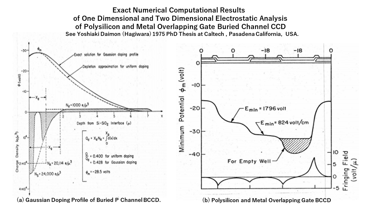
Hagiwara also received the Sony Central Research Center Crystal Award in 1978
for his image sensor time and space spectrum analysis.
++++++++++++++++++++++++++++++++++++++++++++++++++++++++
The Evidence that Yoshiaki Hagiwara at Sony Invented Pinned Photodiode in 1975.
++++++++++++++++++++++++++++++++++++++++++++++++++++++++
Dear Sir
Your honest, free and neutral opinion on the history of invention
and development efforts of image sensors is very important.
The truth should be revealed to all of the people in the world.
You are just one of them. But each one is very, very important.
I summarized my point of view on the history of the invention and the development efforts
of Pinned Photodiode. When I jointed SONY in 1975 after receiving PhD from Caltech, Sony
people understood the importance of the CCD complete charge transfer operation and the
excellent feature of no image lag in the CCD/MOS dynamic photo capacitors. However
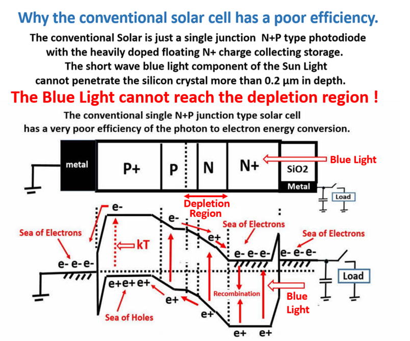
Sony was suffering the yield problem due to the strong surface electric field and the
poor short wave blue light sensitivity since the CCD/MOS dynamic photo capacitors have
the metallic polysilicon electrodes which do not pass the short wave blue light. As you may
know the short wave blue light cannot penetrate more than 0.1 micro meter in depth in
the silicon crystal. The double dynamic photo transistor and the triple junction photo
thyristor were the answers which do not have the surface electric field nor the metallic
electrodes. I applied Japanese patents JP1975-127646, JP1975-127647 and JP1975-134985.
The proposed photodiodes were intended to be applied to the interline CCD image sensors
as explained in my Japanese 1975 patents . I developed the P+NP double junction type photodiode
in 1978 used it in the FT CCD image sensors and reported at SSDM1978 conference in Tokyo.
After that , SONY kept silent since it was a top secrete project in SONY. SONY took more than
8 years to develop and make the passport size portable video cameras with the P+NPN triple
junction type photodiode with the in-pixel overflow drain with the complete electrical
shutter function for action pictures. Sony was only the maker who could produce the camera.
I summarized the details in the site shown below. The problem was that I forgot completely
myself the details of my 1975 inventions since I was busy since 1980 in developing the system
LSI chip sets such as for the SONY AIBO robots and the PS2 and PS3 Play Station Game Machines.
I uploaded here the complete form of my point of view on the PPD invention and development efforts.
I wish people would kindly read this for me and let me know what they think about this.
I am not asking your opinion on the patent issues. Patent issues
were already settled and no problems. Sony is now enjoying the
image sensor business being protected by Hagiwara 1975 Pinned
Photodiode patents. KODAK , NEC and Fairchild also did apply
similar PPD patents. But they were all applied later than 1975.
I am asking your opinion on who is the inventor and who
first developed Pinned Photodiode and reported in the
international technical conference.
These facts are important for the history of image sensors and
have very important meanings as back ground information
and for educational purpose for young generations who
may have interest in image sensors and its history.
The SSDM1978 Conference held in Tokyo in 1978 is also an
international conference but with a very limited number.
The published SSDM1978 conference journal paper is not widely accessed.
But Albert Theuwissen found my SSDM1978 paper after 18 years
and quoted my original 1978 PPD work in his IEEE2006 paper.
Albert Theuwissen did not emphasize the complete charge transfer feature of
Pinned Photodiode since CCD has already the complete charge transfer feature.
The complete charge transfer feature was nothing new.
The importance of Pinned Photodiode were
(1) The excellent short wave blue sensitivity and
(2) the Low Surface Dark Current.
Firstly, since CCD has the metal electrode, it has a poor short wave
blue light sensitivity.
Secondly, the CCD/MOS dynamic photo capacitor has a strong surface electric field
which induces the undesired surface dark current.
However, Albert Theuwissen apparently and SONY( Hagiwara) already understood
the feature of the complete charge Transfer mode of Pinned Photodiode.
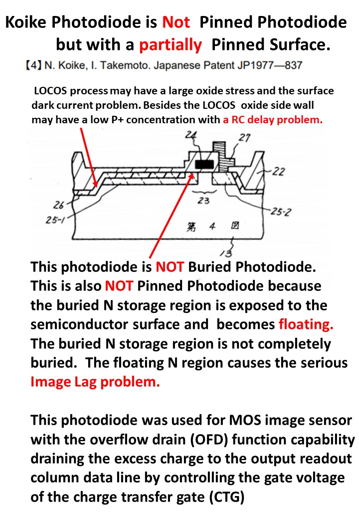
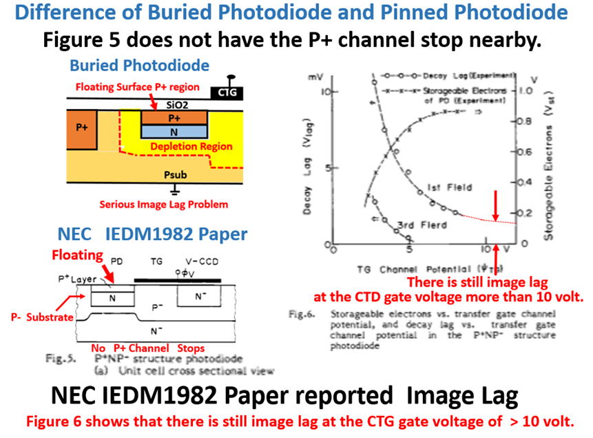
NEC IEDM1982 paper by Teranishi reported the importance of the image lag feature
of Buried Photodiode. But Buried Photodiode is not always Pinned Photodiode.
NEC IEDM1982 paper by Teranishi also reported the serious undesired image lag
feature of the NEC1982 Buried Photodiode in the IEDM1982 paper. Any photodiode
with image lag feature is not Pinned Photodiode according to the Fossum Paper.
Hence NEC IEDM1982 paper was not Pinned Photodiode by definition.
The Difference of Pinned Photodiode and Buried Photodiode was well explained in
the article which says ,"...acknowledge Hagiwara-san's contribution.It has long
been incorrectly attributed to Teranishi and to Fossum (in CMOS image sensors)"
"A pinned PD is designed to have the collection region deplete out when reset.
AS the PD depletes it becomes disconnected from the readout circuit and
if designed properly will drain all charge out of the collection region
(accomplishing complete charge transfer). An interesting side effect is
that the capacitance of the PD drops to effectively zero and therefore
the KTC noise qn=sqrt(KTC) also goes to zero. When you design the depletion
of the PD to deplete at a certain voltage you are pinning that PD to that
voltage. That is where the term comes from. I've edited this Answer to
acknowledge Hagiwara-san's contribution. It has long been incorrectly
attributed to Teranishi and to Fossum (in CMOS image sensors)"
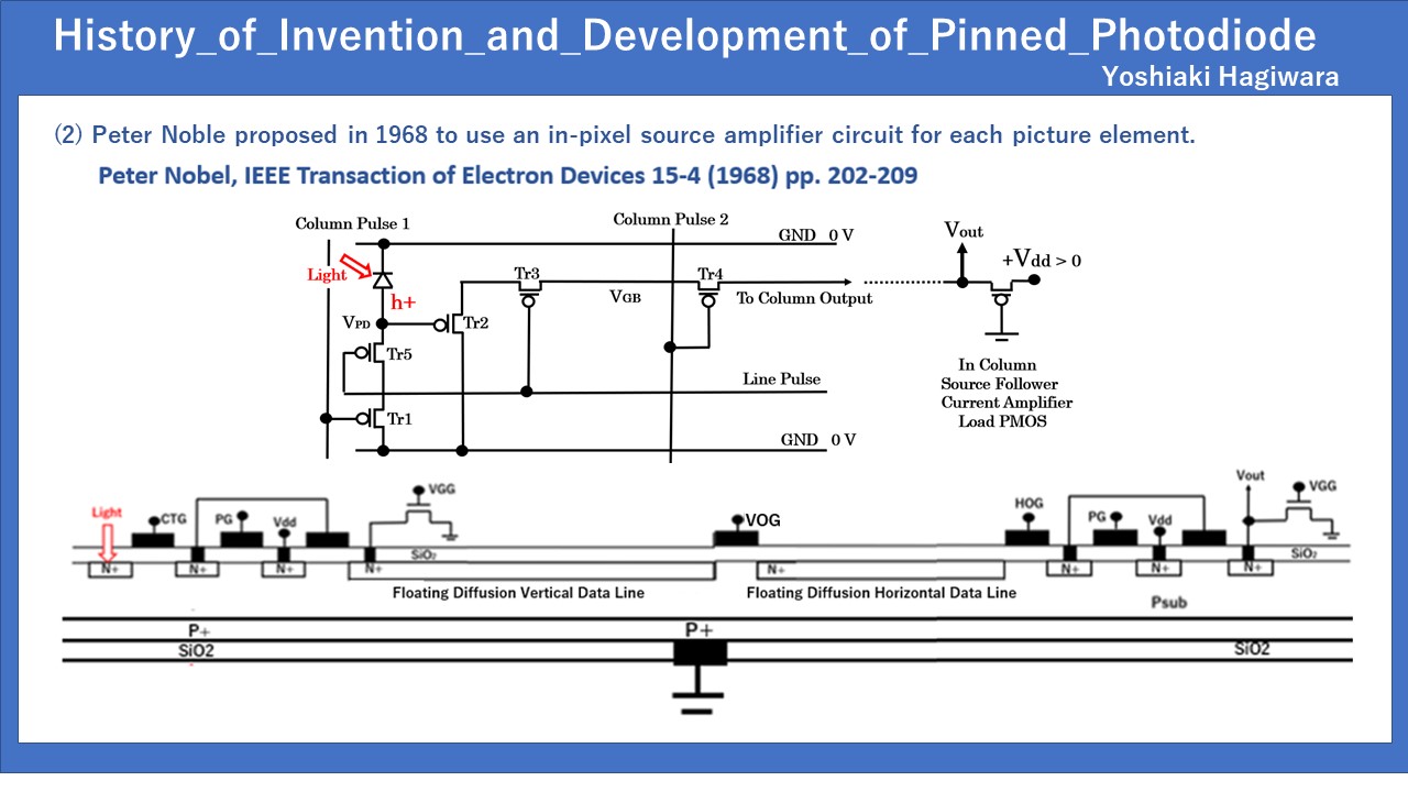
Actually the in-pixel active sensor was first invented and reported
in 1968 by Peter Noble at Plessy in England UK before Fossum work in 1990.
These truth was not well understood widely.
Teranishi and Fossum are well received to the world for their contributions.
But they never quoted Hagiwara and Noble previous old works.
The people misunderstood that Teranishi and Fossum were
the first inventors and the first developers.
Patent issues are settled and now Sony enjoy the image
Sensor business with advantage over KODAK, NEC ,
Fairchild and other competing companies. Sony has
Hole Accumulation Diode (HAD) which is identical to
Pinned Photodiode in the world wide business with
more than 60 to 70 % share of image sensor devices.
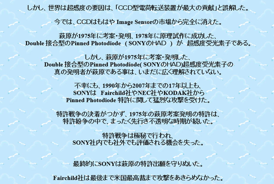
Now the KODAK-named Pinned Photodiode reported in IEDM1984
is now considered as the invention by Teranishi at NEC in 1980,
according to the paper "A Review of the Pinned Photodiode
for CCD and CMOS Image Sensors" by E.Fossum. This Fossum
paper was attacking Hagiwara 1975 patent and SSDM1978
paper with misleading descriptions on no image lag issue.
Hagiwara 1975 patent and SSDM1978 paper did report the
complete charge transfer operation and showed the empty
potential well profile which are signs of no image lag feature.
The truth is that Hagiwara proposed 1975 the now-called
Pinned Photodiode in form of the double PNP and triple PNPN
junction dynamic photodiodes originally.
The double PNP and triple PNPN junction dynamic photodiodes
in 1975 and reported the double PNP junction dynamic
photodiode in Hagiwara SSDM1978 paper.
The patent issues were settled and no problems.
In the secret patent disputes and the public US courts ,
Fairchild, KODAK, NEC in the past attacked Sony on the
basic Pinned Photodiode patents but they were all not
successful. NEC gave up image sensor business and
Fairchild and KODAK made friendly technical agreements
with Sony now. I am not asking about the patent issue.
I need to hear your personal opinion on the historical background
of the invention and the Innovation efforts of Pinned Photodiode.
The truth should be revealed to all of the people in the world.
You are just one of them. But each one is very, very important to me.
Fossum paper claims that Hagiwara JPA1975-134984 and
Hagiwara 1978 paper did not describe the image lag feature.
I believe Fossum misunderstood my 1975 patent and 1978 paper.
Hagiwara JPA1975-134984 showed an empty potential of
the buried N storage region of the double junction PNP
dynamic photo transistor structure with the emitter and
the collector terminals both pinned, which is identical to
Pinned Photodiode. As you know the empty potential well
implies the complete charge transfer operation which results
in the excellent feature of no image lag in video camera.
Hagiwara SSDM1978 paper reported the output wave forms of
the image sensor using the double PNP junction photodiode
with the pinned P+ surface region directly connected to
the adjacent P+ channel stops, which is also identical to
the definition of Pinned Photodiode. The output wave forms
showed a very low total surface dark current of less than 3%
and the complete charge transfer efficiency of more than 99.995%
which implies the excellent feature of no image lag.
My work was cited in "A Review of the Pinned Photodiode for CCD
and CMOS Image Sensors" by E.Fossum. Actually E.Fossum was
attacking my 1975 PPD patent and SSDM1978 PPD paper.
Please kindly read carefully Fossum paper. Fossum was not telling
the truth about Hagiwara 1975-134985 patent and Hagiwara
SSDM 1978 paper. Fossum paper was misleading and had a wrong
conclusion.
I have reported the image lag feature of the complete charge
transfer operation both in my 1975 PPD patent and SSDM1978
PPD paper. Fossum did not read carefully or does not understand
the details of my 1975 PPD patent and SSDM1978 PPD paper.
The truth should be revealed to all of the people in the world.
You are just one of them. But each one is very, very important to me.
I would like to hear your personal opinion on this.
For your information, Sony wrote an article
regarding the original invention of Pinned Photodiode
in the Sony Official Homepage:
"In 1975, Sony invented a CCD image sensor that adopted a back-illuminated N+NP+N junction type
and an N+NP+NP junction type Pinned Photodiode (PPD) (Japanese patent application number
1975-127646, 1975-127647 Yoshiaki Hagiwara). In the same year, inspired by such structure,
Sony invented a PNP junction type PPD with VOD (vertical overflow drain) function (Japanese
Patent No. 1215101 Yoshiaki Hagiwara). After that, Sony succeeded in making a principle prototype
of a frame transfer CCD image sensor that adopted the PNP junction type PPD technology, having a
high-impurity-concentration P+ channel stop region formed near a light receiving section by ion
implantation technology for the first time in the world, and its technical paper was presented
at the academic conference, SSDM 1978 (Y. Hagiwara, M. Abe, and C. Okada, "A 380H x 488V CCD
imager with narrow channel transfer gates", Proc. The 10th Conference on Solid State Devices,
Tokyo, (1978)). In 1980, Sony succeeded in making a camera integrated VTR which incorporated
a one-chip frame transfer CCD image sensor that adopted the PNP junction type PPD. President
Iwama in Tokyo, Chairperson Morita in New York, at the time held a press conference respectively
on the same day, which surprised the world. In 1987, Sony succeeded in developing a 8 mm video
camcorder that adopted, for the first time in the world, the interline transfer CCD image sensor,
which incorporated "PPD having a high-impurity-concentration P+ channel stop region formed near
the light receiving section by ion implantation technology" with VOD function, and became the
pioneer of the video camera market. The PPD technology that has been nurtured through such a
long history is still used in back-illuminated CMOS image sensors."
The Society of Semiconductor Industry Specialists (SSIS) of Japan
Society of Semiconductor Industry Specialists (ssis.or.jp)
also wrote an article regarding the original invention of Pinned Photodiode
on the SSIS official Homepage:
The Society of Semiconductor Industry Specialists (SSIS) of Japan explained
and claimed in details as
"The Pinned Photodiode is a photodiode in which the entire N layer is
covered with a P layer. The part of the P layer on the light incident
surface is heavily doped P+. Kodak named this structure Pinned Photodiode
in 1984 because the P+ surface of the light incident surface was pinned
to the substrate potential.
This device has features such as high light sensitivity, wide dynamic range,
image lag free, much smaller dark current due to reduced influence of GR center
on the light receiving surface, and no white scars.
In 1975, Sony proposed using a PNP transistor as the photodetector [3].
By providing a P+ layer (emitter) for the light incident section,
the sensor electrode that covers the entire light receiving surface of
the photodiode can be eliminated to improve the light sensitivity greatly.
It was a basic proposal for a pinned photodiode with a P+ layer on the surface
of the light receiving part."
The reference [3] is my original Japanese Patent on Pinned Photodiode.
The photodiode structure was originally defined as the double PNP dynamic photo transistor
and the triple junction PNPN dynamic photo thyristor in my patent application Jp1975-134985.
The structure was later called as Buried Photodiode by NEC in 1982, Pinned Photodiode by KODAK in 1984,
and as the Hole Accumulation Diode (HAD) by Sony in 1987.
But all of them are identical to my 1975 invention.
I believe I am the inventor of Pinned Photodiode in 1975 and developed Pinned Photodiode in 1978.
And Sony built the video movie camera used Pinned Photodiode
in the one chip NTSC full size Frame Transfer CCD image sensor in 1980
The details of my works are explained in the following publications.
Would you kindly read my papers and let me know your personal opinion on
who really invented Pinned Photodiode and developed it for the first time in the world ?
++++++++++++++++++++++++++++++++++++++++++++++++++++++++
Paper Accepted with a minor revision. Reviews' Comments:
++++++++++++++++++++++++++++++++++++++++++++++++++++++++
"This is a comprehensive paper, well designed, performed and written.
The logicality of this paper is quite good and the main body provides
sufficient information. The study abstract is concise and clearly presented,
and the figures in the article have well illustrated the study. Meanwhile,
the author gives a comprehensive description in conclusion.
This is a very instructive research. It is suggested that recommendations
for follow-up or future work on this topic should be made."
+++++++++++++++++++++++++++++++++++++++++++++++++++++++++
List of Related Published Papers on Pinned Photodiode
+++++++++++++++++++++++++++++++++++++++++++++++++++++++++
Unfortunately these Japanese Patent Applications of mine shown below were
written only in Japanese language and were never disclosed in details to
the English Speaking Community.
++++++++++++++++++++++++++++++++++++++++++++++++++++++++++
++++++++++++++++++++++++++++++++++++++++++++++++
........Bio_of_Yoshiaki_Hagiwara.html...........
++++++++++++++++++++++++++++++++++++++++++++++++
Yoshiaki Hagiwara wrote a book on "the World of Artificial Intelligent Digital Circuits",
which is important and needed to built the intelligent image sensor systems.
(8) Visiting Professorship in Electric Engineering Department and
Applied Physics Department at California Institute of Technology,
Pasadena, califor, USA, 1998-1999;https://www.caltech.edu/
(9) Professorship in Electircal Engineering Department at Gunma University,
Kiryu-city, Gunma-ken, Japan, 2001-2008;https://www.gunma-u.ac.jp/
(10) Professorship in Information and Communication Tecnology Department
at Sojo University, Kumamoto-city, Japan, 2009-2017; https://www.sojo-u.ac.jp/
(11) Artificial Intelligent Partner System (AIPS) Consortium,Kanagawa-ken NPO, Japan,
President and CEO (2008-2017); http://www.aiplab.com//
++++++++++++++++++++++++++++++++++++++++++++++++
........Bio_of_Yoshiaki_Hagiwara.html...........
++++++++++++++++++++++++++++++++++++++++++++++++
Yoshiaki Hagiwara wrote a book on "the World of Artificial Intelligent Digital Circuits",
which is important and needed to built the intelligent image sensor systems.
(8) Visiting Professorship in Electric Engineering Department and
Applied Physics Department at California Institute of Technology,
Pasadena, califor, USA, 1998-1999;https://www.caltech.edu/
(9) Professorship in Electircal Engineering Department at Gunma University,
Kiryu-city, Gunma-ken, Japan, 2001-2008;https://www.gunma-u.ac.jp/
(10) Professorship in Information and Communication Tecnology Department
at Sojo University, Kumamoto-city, Japan, 2009-2017; https://www.sojo-u.ac.jp/
(11) Artificial Intelligent Partner System (AIPS) Consortium,Kanagawa-ken NPO, Japan,
President and CEO (2008-2017); http://www.aiplab.com//


.jpg)