++++++++++++++++++++++++++++++++++++++++++++++++ Back Slide ...
First Slide ...
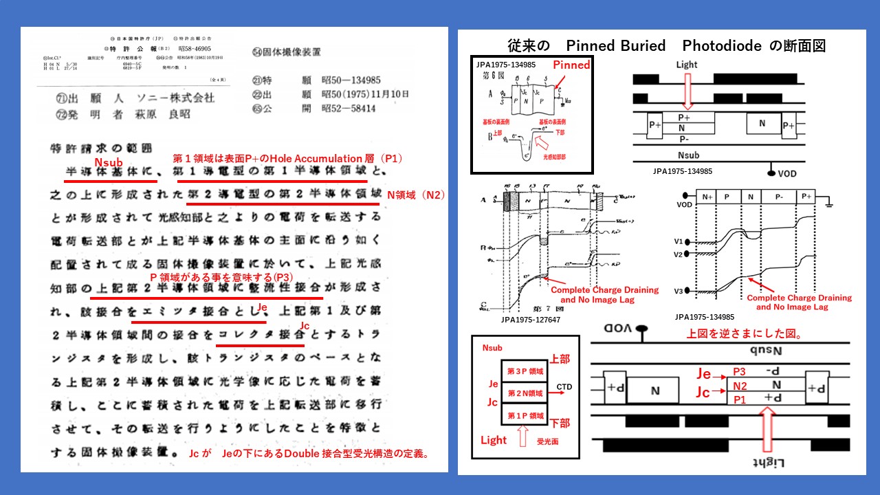
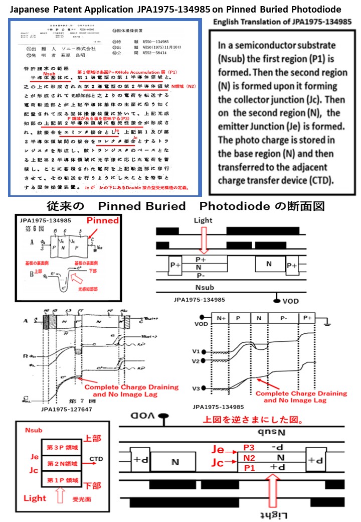
SlideP007.pdf JPA_1975_134985_Pinned_Buried_Photodiode_with_VOD.pdf JPA1975-134985_PNP_double_junction_Pinned_Buried_Photodidode_invented_by_Yoshiaki_Hagiwara_at_Sony_19751110.pdf JPA1975-134985_English_Translation.pdf JPA_1975_134985_Pinned_Buried_Photodiode_with_VOD_007A.pdf Who_invented_Pinned_Photodiode_?_Yoshiaki_Hagiwara.html 001..
002..
003..
004..
005..
006..
007..
008..
009..
010.. 011..
012..
013..
014..
015..
016..
XXX.. Sony_vs_Loral_Patent_War_1_Reviews.pdf Sony_vs_Loral_Patent_War_2_Supporting_Opinions.pdf E-mail_Communication_on_Sony_Loral_Patent_War_1996.pdf E-mail_communication_with_Albert_san_2018_07_10.pdf HAD_sensor_NEC_SONY_Patent_War.pdf JP1980_138026_NEC_Buried_Photodiode_Patent.pdf JP1978-1971_Toshiba_Yamada_VOD_patent.pdf Sony_vs_Loral_PAtent_War_13_pages.pdf Sony_vs_Loral_Patent_War_53_pages.pdf Image_Sensor_Story_by_Hagiwara.pdf The_evidence_that_Hagiwara_is_the_inventor_of_Pinned_Photodiode_7_pages.pdf Future_of_Image_Sensors_and_Solar_Cells.pdf JP1975-127646_NPNP_triple_junction_Pinned_Photodiode_Patent_32_pages.pdf The_First_Pinned_Photodiode_was_invented_in_1975_by_Yoshiaki_Hagiwar_at_Sony.pdf JP1975-127647_NPN_double_junction_Pinned_Photodiode_Patent_22_pages.pdf JP1975-134985_PNP_double_junction_Pinned_Photodiode_on_Nsub_Patent_7_pages.pdf JP1977-126885_Elecric_Shutter_Clocking_Scheme_by_OFD_Punch_Thru_Action_13_pages.pdf JP2014-135497_Digital_Transformation_Circuit_for_Image_Sensors_29_pages.pdf JP2020_131313_on_Doubel_Junction_Pinned_Photodiode_Solar_Cell_65_Pages.pdf P1978_Pinned_Photodiode_1978_Paper_by_Hagiwara_7_Pages.pdf P1996_Pinned_Photodidoe_used_in_Sony_1980_FT_CCD_Image_Sensor_9_Pages.pdf P2001_ESSCIRC2001_Micro-Electronics_for_Home_Entertainment_11_pages.pdf P2008_ESSCIRC_2008_SOI_Design_in_Cell_Processor_and_Beyond_7_pages.pdf P2013_ISSCC2013_Panel_Talk_25_pages.pdf P2017_CoolChips_Panel_170419_29_pages.pdf P2019_3DIC2019_Paper_on_3D_Pinned_Photodiode_6_pages.pdf P2020_EDTM2020_PaperID_3C4_by_Hagiwara_4_pages.pdf P2021_IJSSA2021_Paper_20210616_on_Electrostatic_and_Dynamic_Analysis_of_Pinned_Photodiodes.pdf Buried_Photodiode_is_not_always_PPD_Hagiwara_Nov_2020.pdf Caltech_1975_PhD_Thesis_Yoshiaki_Daimon_Hagihara.pdf Difference_of_Buried_Photodiode_and_Pinned_Photodiode.pdf E-mail_Communication_on_Sony_Loral_Patent_War_1996.pdf E-mail_communication_with_Albert_and_Yoshi.pdf E-mail_communication_with_Albert_san_2018_07_10.pdf E-mail_communication_with_Albert_san_2018_07_10A.pdf E-mail_communication_with_Albert_san_2018_07_10B.pdf Evidence_that_Hagiwara_is_the_inventor_of_Pinned_Photodiode_2020_10_04a.pdf Evidence_that_Hagiwara_is_the_inventor_of_Pinned_Photodiode_in_Japanese.pdf Future_of_Image_Sensors_and_Solar_Cells .pdf Hagiwara_at_Sony_invented_in_1975_and_developed_Pinned_Photodiode_in_1978.pdf http://www.aiplab.com