**********************
AIPS ( Artificial Intelligent Partner System ) Homepage Z000
hagiwara-yoshiaki@aiplab.com
**********************
**********************
これは70歳じじいのぶつぶつぼやきの独り言です。
**********************
●日本半導体産業人協会(SSIS)の教育委員会委員として
奉仕しています。また、春と秋に開催の半導体技術講座で、
「イメージセンサー賢い目」の講師として奉仕しています。
●韓ドラを見ながら、ハングルを学習しはじめました。
●中学数学でわかる「特殊相対性理論」
●小学校の算数の問題「油わけ算数」
**********************
*************************
萩原良昭著書の紹介です:
「人工知能を支える、デジタル回路の世界」
萩原1975年特許の画像
******************************
Pinned_Photodiode_and_SONY_HAD_Sensor_invented_by_Hagiwara.pdf
******************************
Index_A000 Story_of_Pinned_Photo_Diode.html
Index_A001 半導体は現代文明のエンジン
Index_A002 「賢い電子の目」のお話
Index_A003 Image Sensor の基本構造
Index_A004 History of Photodiode
Index_A005 種々の半導体受光素子( Photodiode )
Index_A006 1975年2月SONYに入社して
Index_A007 なぜ CCD Image Sensor が消えたのか?
Index_A008 埋め込みPhotodiode と Pinned Photodiodeの違いは何か?
Index_A009 Device Physics of Pinned Photo Diode.html
****************************
Yoshiaki Hagiwara was invited in the following five international
conferences because of his contributions to the image sensor
community and related digital system LSI chip design works.
See the five invited talks related to the Pinned Photo Diode
which is also called as SONY original Hole Accumulation
Diode (HAD) image sensor.
(1) International Conference CCD79 in Edinburgh, Scotland UK
See http://www.aiplab.com/0-CCD79_1979Hagiwara.pdf
(2) International Conference ESSCIRC2001 in Vilach, Austria.
See http://www.aiplab.com/ESSCIRC2001.pdf
(3) International Conference ESSCIRC2008 in Edinburgh, Scotland UK
See http://www.aiplab.com/0-ESSCIRC2008Hagiwara.pdf
(4) International Conference ISSCC2013 in San Francisco, California USA
See http://www.aiplab.com/ ISSCC2013PanelTalk.pdf
(5) IEEE Computer Society 主催の Coolchips 2017 at Yokohama, Japan
See http://www.coolchips.org/2017/?page_id=10#panel
Related Works by Hagiwara
(1) Pinned Photo Diode (P+NP) and SONY HAD
(P+NPNsub) are the same thing. Both were invented
by Hagiwara at Sony in 1975 in the Japanese Patents
See http://www.aiplab.com/Pinned_Photo_Diode_1975_invented_by_Hagiwara.pdf
(2) For MOS CTG Global Shutter Memory and Back Light Illumination
PP-NP+N-N+ junction Pinned Photodiode Patent ,
see http://www.aiplab.com/JP1975-127646.pdf
(3) For MOS CTG Global Shutter Memory and Back Light Illumination
NP+N-N+ junction Pinned Photodiode Patent,
see http://www.aiplab.com/JP1975-127647.pdf
(4) For the built-in Vertical Overflow Drain (VOD) function type
P+NPNsub junction Pinned Photodiode Patent,
see http://www.aiplab.com/JP1975-134985.pdf
(5) Hagiwara as a PhD student at CalTech designed
a Fast 128 bit digital data stream parallel comparator
chip, which was fabricated at Intel with the Intel 1101
PMOS process technology.
See http://www.aiplab.com/128_bit_Comparator.pdf
(6) Hagiwara designed a Fast 25 nanosecond access time
4 M bit Cache SRAM chip for digital camera applications.
Intel used the SONY SRAM chips in the Intel boards.
Sony enjoyed SRAM business while many semiconductor
companies in Japan were focusing on the 4 M bit DRAM
chip business.
See http://www.aiplab.com/SONY_4MSRAM_1989.pdf
**********************
.
****************************
More about Appendix Page List
****************************
000 001 002 003 004 005 006 007 008 009 010
011 012 013 014 015 016 017 018(Ref) 019 020
021 022 023 024 025 026 027 028 029 030 031 032
033 034 035 036 037 038 039 040 041 042 043
****************************
Device Physics of Pinned Photodiode
JP 1975-127646.pfd
JAP 1975-127647.html
JP 1975-127647.pdf
JAP 1975-134985.html
JP 1975-134985.pdf
JP 1978-1971.pdf
JP 1980-123259.pdf
List.html
index000.html
index000_ImageSensor.html
index_000_introduction.html
index_001_Sony_HAD_senosor.html
indexAIPS.html
indexAIPS01.html
indexA1_What_is_Semiconductor.html
indexA2_What_is_Solar_Cell.html
indexA3_What_is_Solid_State_Image_Semsor.html
indexHADsensor.html
indexHADsensor01.html
index_Hagiwara_Diode.html
index_Fossum_is_a_liar.html
index001_introduction.html
index001_Introduction_of_Hagiwara.html
index002_SONY_original_HAD_sensor.html
index002_What_is_Pinned_Photo_Diode.html
index003_PPD_and_HAD_are_the_same_thing.html
index003_What_is_Digital_Camera_Made_OF
index004_Hagiwara_invented_Pinned_Photo_Diode.html
index004_Hagiwara_Works.html
index005_Hagiwara_1975_Patent.html
index005_Semionductor_Device_Physics_for_PPD.html
index006_Sony_Fairchild_Patent_War.html
index006_Two_1975_Hagiwara_Patents_on_Pinned_Photo_Diode.html
index007_Sony_NEC_Patent_War.html
index007_Two_Japanese_1975_Patents_on_Pinned_Photo_Diode
index008_Fossum_2014_Fake_Paper.html
index008_How_Hagiwara_PPD_Patents_Saved_SONY_Business
index009_Summary.html
Hagiwara_at_Sony_is_the_true_inventor_of_Pinned_Photo_Diode.html
Page001.html
Page002.html
Page003.html
Page004.html
Page005.html
Page006.html
Page007.html
Page008.html
Page009.html
Page010.html
Page011.html
Page012.html
Page013.html
Page100.html
Ref1.html
Ref2.html
Ref3.html
Ref4.html
Ref5.html
Ref6.html
Ref7.html
Story_of_Pinned_Photo_Diode.html
Study_Korean.html
index_A3_1_2_Special_Relativity.html
index_Abura_Wake_Zan.html
index_TsuruKameZan.html
index_01_KisoJouhoSuugaku.html
index_02_OuyouJouhoSuugaku.html
index_03_SuuchiKeisanHou.html
index_04_DigitalCircuits.html
index_05_SemiconductorLSI.html
index_06_RobotKougakuKiso.html
index0-1-1.html
index0-1-2.html
index0-1-3.html
index0-1-4.html
index0-1-5.html
index0-1-6.html
index0-1-7.html
index0-1-8.html
index0-1-9.html
index0-1-10.html
index0-1-11.html
index0-1-12.html
index0-1-13.html
index0-1-14.html
index0-1-15.html
index0-1-16.html
index0-2-1.html
index0-2-2.html
index0-2-3.html
index0-2-4.html
index0-2-5.html
index0-2-6.html
index0-2-7.html
index0-2-8.html
index0-2-9.html
index1-2-1.html
index000_KAIT01.html
index000_KAIT02.html
index000_KAIT03.html
Pinned_Photodiode_and_SONY_HAD_Sensor_invented_by_Hagiwara.pdf
0-CCD79_1979Hagiwara.pdf
0-ESSCIRC2008Hagiwara.pdf
0-HAD_Sensor_Patent_1975Hagiwara.pdf
128_bit_Comparator.pdf
HADsensor_NEC_SONY_Patent.pdf
Hagiwara_invented_pinned_photo_diode_in_1975_01.pdf
JPL_CalTech_Pain.pdf
Pinned_Photo_Diode_1975_invented_by_Hagiwara.pdf
Pinned_Photo_Diode_Patent_by_Hagiwara_at_Sony_in_1975.pdf
Pinned_Photodiode_1978_Paper_by_Hagiwara.pdf
Pinned_Photodiode_Patents_1975.pdf
Hagiwara_Yoshiaki_CaltechDiploma_PhD1975.pdf
**********************
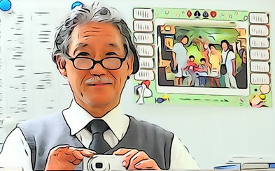
The AIPS image sensor watching at its inventor, Yoshiaki Hagiwara.
return to the TOP Page
**********************