****************************************************
AIPS ( Artificial Intelligent Partner System ) Homepage A008
hagiwara-yoshiaki@aiplab.com
*******************************************************
埋め込みPhotodiode と Pinned Photodiodeの違いは何か?
*******************************************************
*******************************************************
埋め込みPhotodiode と Pinned Photodiodeの違いは何か?
*******************************************************
Do you know the difference of Buried and Pinned Photodiode ?
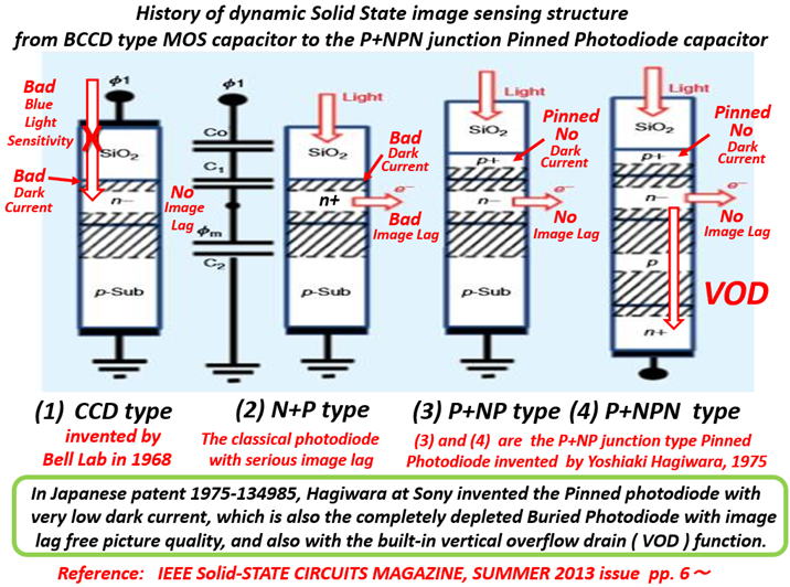
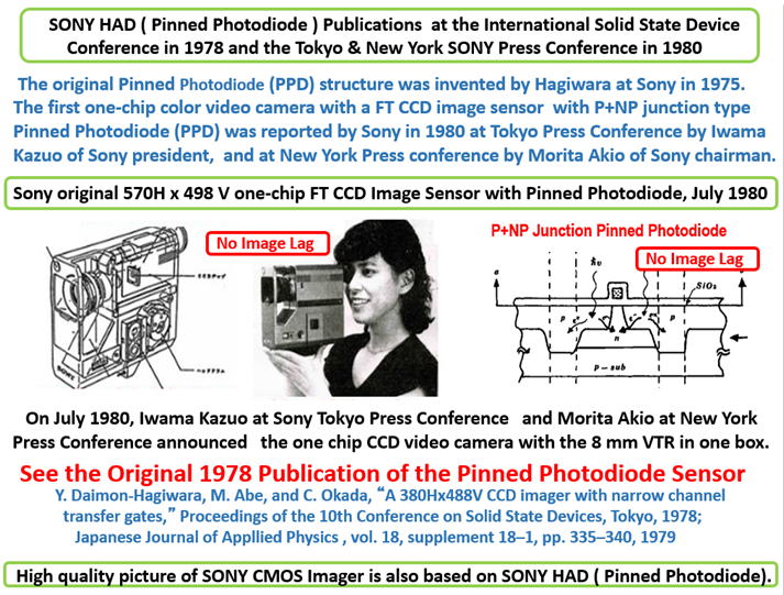
萩原は1980年にSONYで透明電極を使ったCCD型のMOS容量の受光素子
を開発し、Interline方式のCCD image sensorに採用しました。そして、
高速アクション映像を可能にする、残像のない映像を実現しました。
Hagiwara at Sony developed the transparent CCD type MOS capacitor
photodiode for the interline transfer CCD image sensor in 1980, which
gives the image lag free feature for the fast action picture quality.
埋め込み型とピン留め型の受光素子の違いはたいへん重要です。完全
信号電荷空乏化した受光素子の動作は残像のない映像を提供できます
が、しかしそれ以上の機能はありません。まだまだ問題があります。
The differnce between the buried potodiode and the pinned photodiode
is very important. The buried photodiode with the completed depletetion
mode provides also the image lag free pictures. But that was not enough.
その理由は、シリコン結晶と酸化膜の間の界面に存在する正の電荷を
帯びた界面準位 Qss による表面電界が表面暗電流を発生する為です。
The reason is the positive fixed silicon-oxide interface charge +Qss
that casuses surface electric field and results in serious dark current.
この+Qssの電荷のバラツキが局所的に大きな暗電流の原因となり
多くの白点が最終映像に現れ、深刻な歩留まり量産問題となります。
This +Qss charge fluctuation often causes the local large serious dark
current spots which give many white point defects in the final pictures.
SONYは透明電極のCCD型MOS容量の受光素子を採用した為に常に
シリコン結晶と酸化膜の界面に電界が存在し深刻な暗電流問題を
かかえてしまい、CCDチップの歩留まりはたいへん低いものでした。
Sony suffered this problem with the transparent CCD type MOS capacitor
photodiode which has strong electric field at the silicon surface, always
causing the serious dark current. The chip yield was very, very low.
そこで萩原はシリコン結晶表面に、2 x 10**13/cm**2 程度のイオン
打ち込みを実施する事を考案しました。その結果、表面に形成された
P+層が、表面の正の固定電荷+Qssの効果を抑圧する事ができました。
Hagiwara proposed to apply the 2 x 10**13 /cm**2 ion implantation
at the silicon surface to create the hole accumulation layer of the P+
region which can quench the surface positive fixed interface charge Qss.
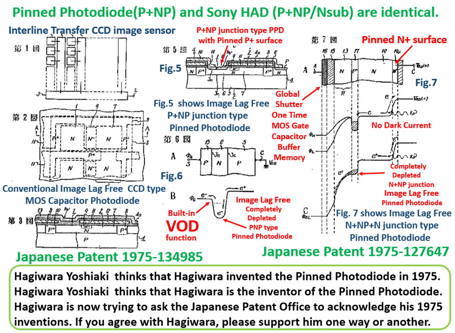
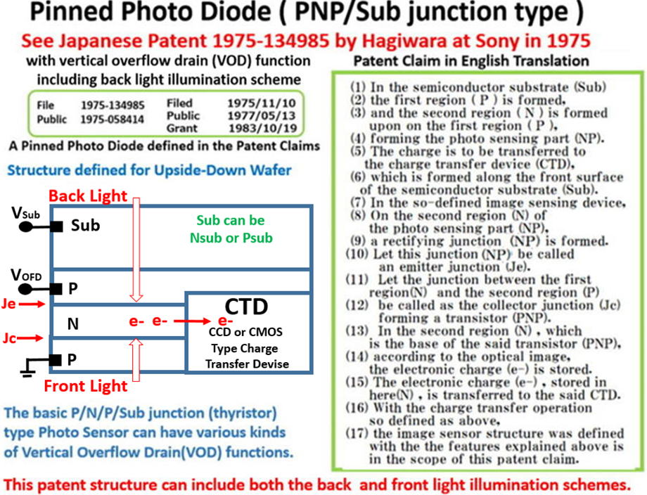
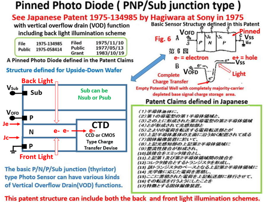
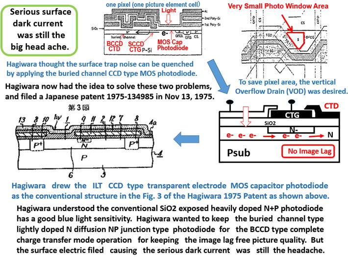
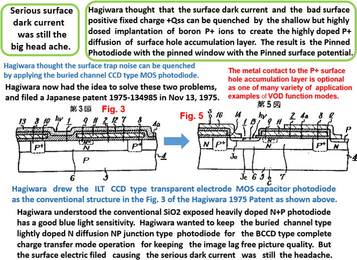
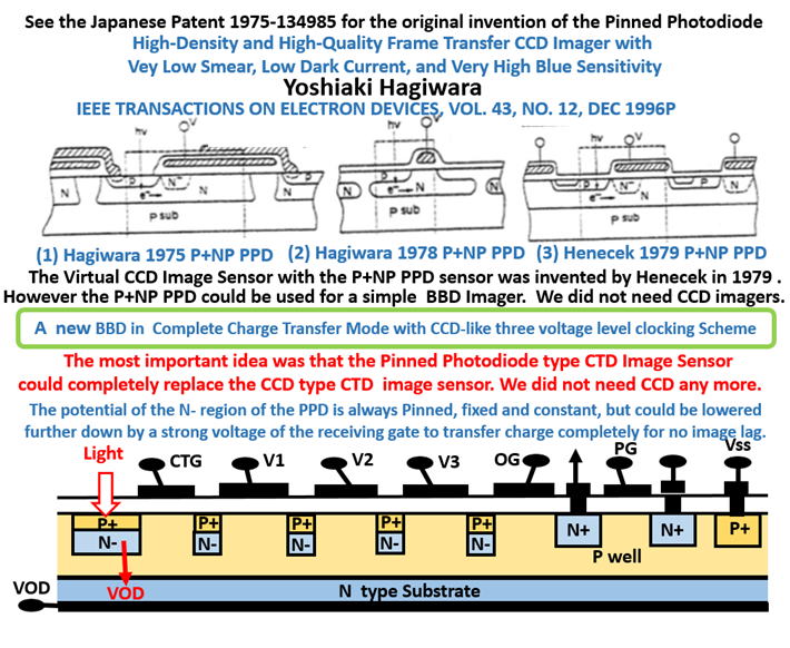
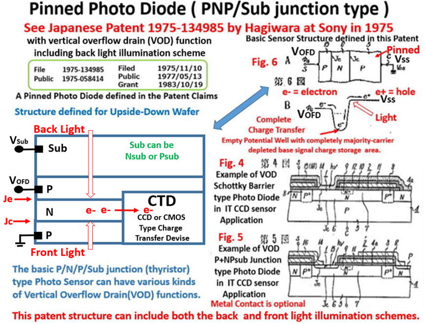
こうして萩原は、日本国特許(昭50-134985)を出願し、暗電流の問題
が全くない P+NPNsub接合型の受光素子を発明しました。
Thus Hagiwara proposed P+NPNsub junction type photodiode with
no dark current problem at all. See Patent 1975-134985 by Hagiwara.
このP+NPNsub接合型受光素子には、次の3つの特徴があります。
This P+NPNsub junction photodiode has three important features.
(1)P+NP接合型受光素子で Pinned Photodiode で、(2)残像のない映像
を提供する完全電荷「空乏化photodiode」の埋め込み photodiode で、
(3)構造上、縦型overflow drain (VOD) 機能が組み込まれたものです。
They are, (1) tthe P+NP junction is Pinned Photodiode, (2) the image
-lag-free complete-deplemon-mode photodiode ( Buried Photodiode)
(3) with the vertical overflow drain (VOD) function.
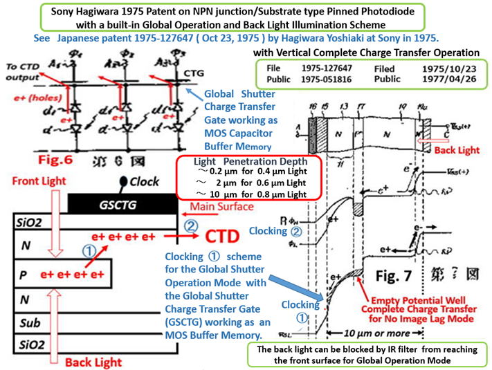
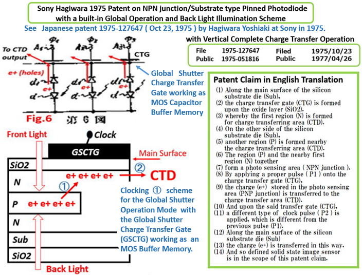
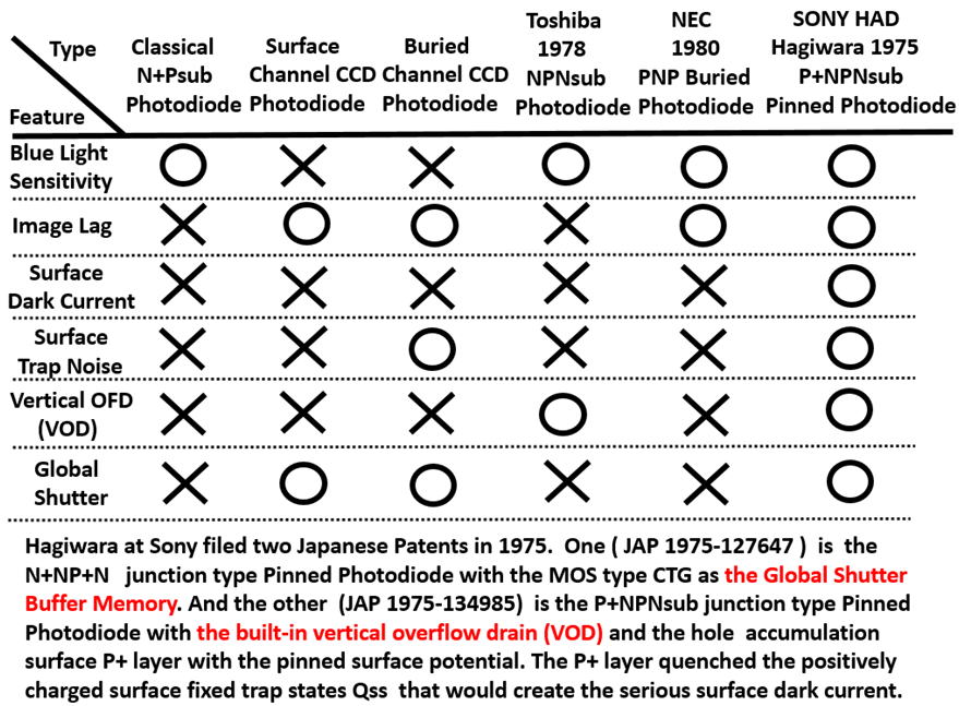
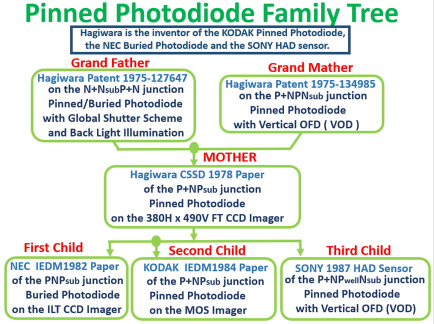
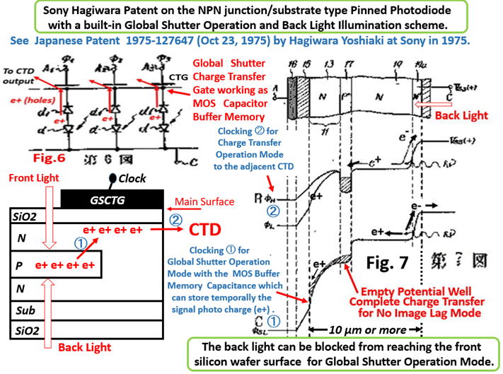
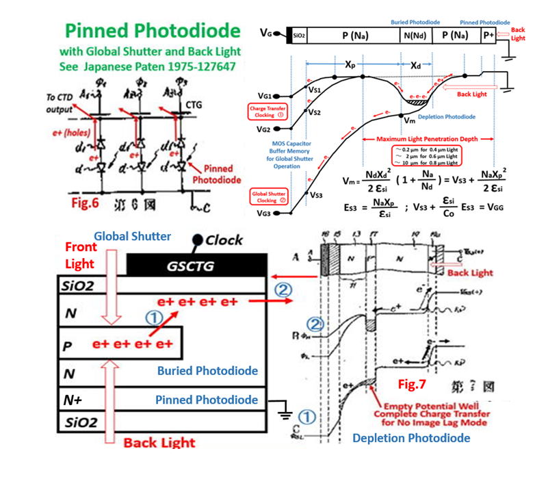
萩原は1975年また同時に、日本国特許( 昭50-127647 ) を出願し2つの
重要な特徴を持つN+NP+N 接合型のPinned Photodiode を発明しました。
In 1975 at the same time Hagiwara also invented the N+NP+N junction
type Pinne Photodiode (1975-127647) with two very important features.
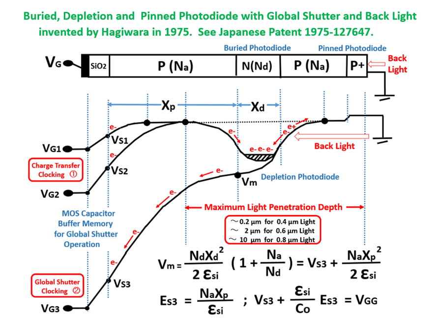
その1つの特徴は、裏面照射型の 埋め込み Photodiode 構造でもある、、
N+NP+N 接合型のPinned Photodiodeであることです。
One of the two important features is the back light illumination scheme
for the N+NP+N junction type Pinned Photodiode, which is also a Buried
Photodiode.
隣接する電荷転送装置(CTD)に、表面型の電荷転送電極(CTG)を
介して、信号電荷を一時的に蓄積する、すなわち、一時メモリ素子
として機能する特別な動作をする構造になっています。
This Hagiwara 1975 invention has a special function mode of one time
memory operation of the sueface type charge transfer gate (CTG) when
the signal photocharge stored in the photodiode is to be transfered
completely to the adjacent charge transfer device (CTD).
裏面照射を実現するには、シリコン結晶ウェーハを薄く研磨する必要
があります。光がシリコン結晶の奥深くまでは透過しないからです。
In order to realize the back light illumination scheme, the silicon wafer
has to be thinned very much because the light cannot penetrate into
the silicon wafer too deeply.
青色の 0.4 um 短波長光では、シリコン結晶を 0.2 um 程度しか
透過しません。0.5 um 波長光では 2 um 程度です。0.6 um の赤色
の波長では 10 um ぐらいまでしか透過しません。従ってシリコン
ウェーハ―を 10um程度に薄く研磨する必要があります。
The blue light of the short light wave length of 0.4 um can penetrate
into the silicon wafer upto the depth of 0.2 um from the silicon wafer
surface. About 2 um depth for the 0.5 um wave length and about
10 um depth for the red light of the 0.6 wave length. Hece silicon
wafer must be thinned upto about the 10 um thickness by polishing.
逆に 10 um 以上程度にしておくと、赤外線カットフィルターを
使用する事により、表側に形成された、電荷転送用電極には裏面
からの照射された光は透過してこない事になり、表側に形成された
一時記憶メモリー容量用の電荷転送用電極は充分 Global Shutter
用の一時メモリーとして機能することになります。
On the contray, by using an infared cut filter, and if the silicon wafer
is kept just about the thickness of above 10 um, the light cannot reach
the fornt side of the silicon wafer, the surface device is completely
blinded and protected form the back light. By doing so, the surface
type charge transfer gate (CTG) MOS capacitor can function properly
as the one time buffer memory for the Global Shutter operation mode.
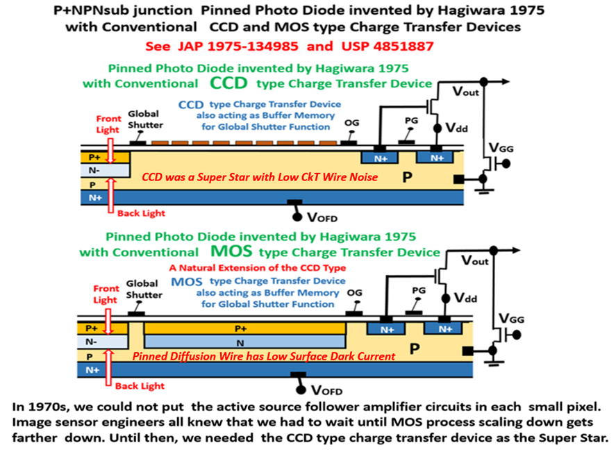
CCD型電荷転送方式のImage sensor は自動的にCCD容量が一時メモリ
素子機能をもち、Global Shutterの機能が組み込まれることは周知です。
It is well known, and it is also the very imprtant feature of the CCD
invention, that the CCD capacitors can act also as one time buffer
memory for the Global Shutter operation mode.
一方、CMOS型電荷転送方式の image sensor では、Global Shutter の
機能を持たせるには、余分な一時メモリ容量が各絵素に必要です。
まだ微細加工技術が進んでいなかった時代では不可能な事でした。
On the other hand, in case of CMOS charge transfer device (CTD) type
image sensors, an expensive one time buffer memory is needed for
each pixel, which could not be affored at all when the MOS process
shrinking technology was not so much advanced in the past years.
しかし、萩原の1975年発明のこの日本国特許 ( 昭50-127647 ) には
すでに、各絵素の表面型電荷転送電極を一時記憶メモリーとして機能
させて、Global Shutter 機能を可能にすることが、その特許請求範囲
に、明確に記載されています。
However, the patent claim of Hagiwara 1975 invention ( Japanese
Patent 1975-127647 ) clearly defined already the surface type
charge transfer gate (CTG) in each pixel unit to be used as the
one time buffer memory for the Global Shutter operation scheme.
CCD 以外では、CMOS 型の電荷転送方式の Image sensor 等の
場合には、Global Shutter 機能を可能にする為には、必ず、一時
記憶メモリ容量が各絵素ごとに必要となることは、周知でした。
It was well understood that, except CCD type CTDs, all other
types of CTDs, such as CMOS type CTD needs one time buffer
memory in each pixel unit for the Global Shutter operation scheme.
萩原が1975年の特許で考案している、この各絵素ごとの表面型の
電荷転送電極(CTG)は、そのGlobal Shutter 機能に必要な、
メモリー容量として機能する事になります。
As Hagiwara proposed in the 1975 patent, this sureface type charge
transfer gate (CTG) in each pixel can act as the one time buffer
memory which is needed for the Global Shutter operation scheme.
従って、萩原の1975年の特許 (昭50-127647) はまた、CMOS Image
Sensor には不可欠な Global Shutter 機能が組み込まれた、Pinned
Photodiode を発明している事になります。
Hence, this means that Hagiwara invented the Pinned Photodiode
structure with Global Shutter function for CMOS image sensors in
the Hagiwara 1975 patent (1975-127647 ).
萩原は、CMOS image sensorに不可欠な、この Global Shutter
の構造と、その動作機能を考案した発明者でもあります。
Hagiwara is the inventor of the Global Shutter structure
and the operation scheme needed in CMOS image sensors.
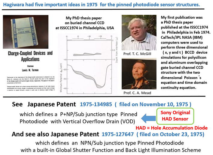
これが萩原の1975年の重要な5つ目の発明となります。
This was the fifth invention of Hagiwara 1975 important inventions.
結論として萩原は5つの重要なアイデアの発明者です。
In summary, Hagiwara is the inventor of the five importat ideas.
.
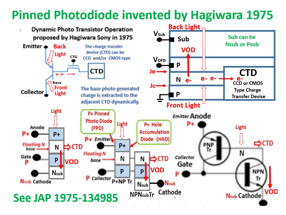
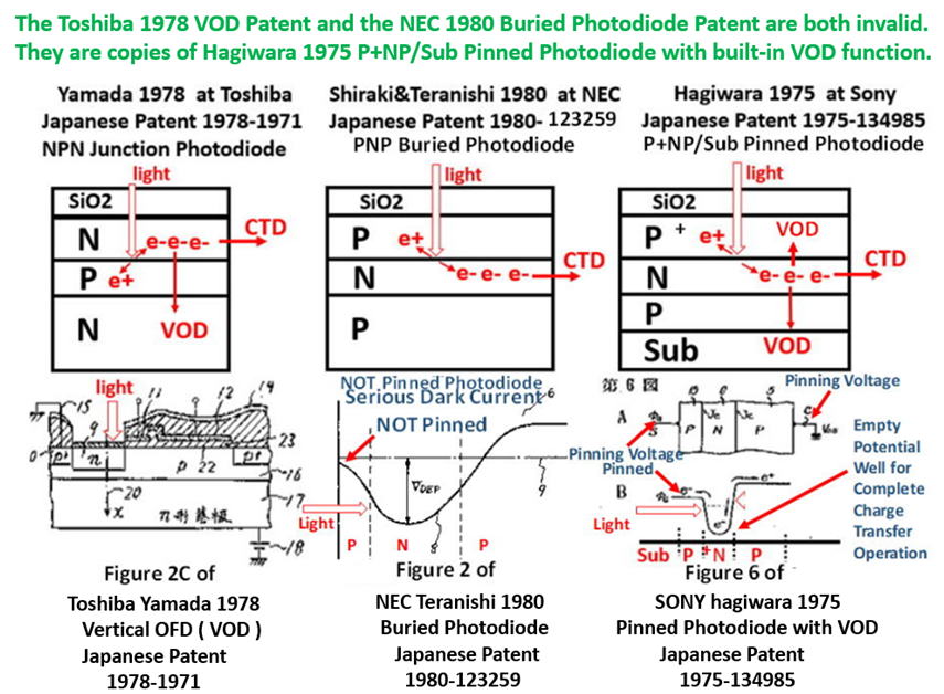
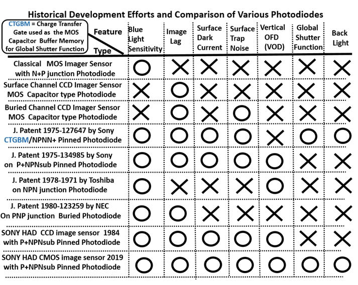
(1)暗電流を抑圧する、 P+NP接合型受光素子、すなわち Pinned Photodiodeの発明です。
The invention of the P+NP junction type Pinned Photodiode with low dark
current.
(2)残像のない映像を可能にする、PNP接型受光素子の「空乏化Photodiode」として
機能する、埋め込みPhotodiodeの発明です。
The invention of the PNP junction type Buried Photodiode with the completely
signal charge depletion that provides the image lag free picture quality.
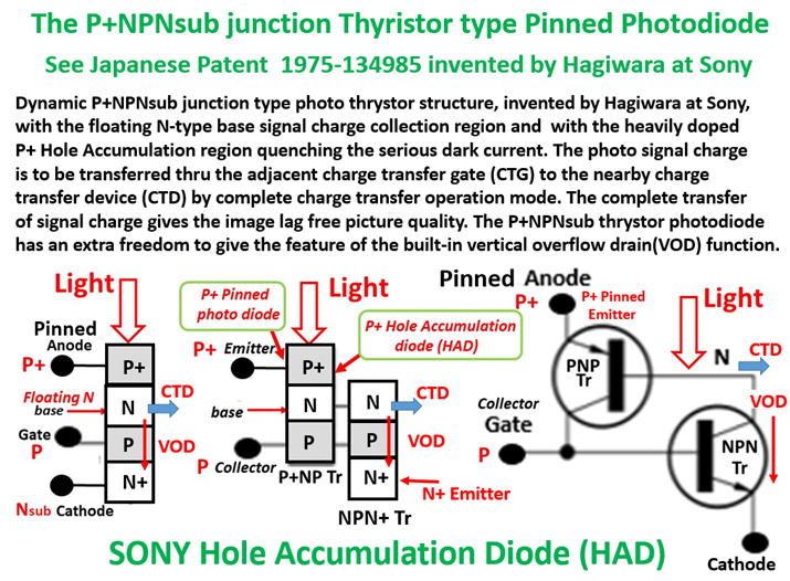
(3)基体(Nsub)に P+NP接合型受光素子を形成し、P+NPNsu接合構造のサイリスタ構造
とすることにより、構造上の動作 mode に自由度が増加し、縦型OFD(VOD)として
も機能することを萩原は特許の中の実施図で明示しています。縦型OFD(VOD)の発明です。
Forming the P+NP junction type Pinned Photodiode on the N-type substrate,
the
resulted P+NPNsub junction thysistor type has a variety of opeation mode
freedom
that include the vertical overflow drain (VOD) operation mode scheme. This
idea
was decribed in the Hagiwara patent figures. This is the invention of the vertical
overflow drain (VOD) by Hagiwara in 1975.
(4)萩原はまた裏面照射型N+NP+N接合型の埋め込みPhotodiodeの発明者でもあり、
Pinned Photodiodeでもある受光素子の発明者です。表側には表面型の電荷転送
電極が、MOS 容量型の、Global Shutter 用の一時 Buffer memory として、掲載
されており実施例には、信号電荷蓄積層から信号電荷が完全空乏化電荷転送
されることを明示しており、この信号電荷蓄積層が残像のない映像を提供する
「空乏化Photodiode」であることを明示しており、萩原は、「空乏化Photodiode」
の発明者でもあります。
Hagiwara is also the inventor of the back light illumination scheme of
the
N+NP+N junction type Buried Photodiode, which is also the Pinned Photodiode.
On the front side of the silicon wafer, as shown in the patent figure, the
surface type charge tansfer gate (CTG) recieves the signal charge from
the
buried photodiode which is shown clealy in the figure completely depleted
of signal charge at the end of the charge transfer to the charge transfer
gate (CTG) which acts as one time MOS capacitor type buffer memory.
The completely depleted buried photodiode provides the image lag free
picture quality. Hagiwara is also the inventor of the completely depleted
buried photodiode with the image lag free picture quality.
(5)萩原はすでに1975年に、可視光線がシリコン結晶体を10um 以上透過
しないことを考慮して、シリコン結晶の膜厚を 10 um 以上程度にする
ことにより、表側の表面電荷転送電極が一時記憶メモリー用容量電極
として充分機能する事を見抜きました。萩原は裏面照射型のPinned
Photodiodeの発明者でもありますが、同時にもうひとつの重要な機能
である、各絵素にBuffer Memoryを持つGlobal Shutter の発明者でも
あります。萩原は世界で初めて、 CMOS Imagerなどで不可欠な、
各絵素に一時記憶メモリー用容量電極を装備することを考案しました。
萩原は、各絵素にBuffer Memoryを持つGlobal Shutter の発明者です。
Hagiwara in 1975 already knew that the visible light cannot penetrate
more than the 10 um silicon wafer depth. So thinning the silicon wafer
just about the thickness of above the 10 um range, the surface type
charge transfer gate (CTG) MOS capacitor can act as the one time
buffer memory for the Global Shutter opertaion scheme. The signal
charge under the one type buffer memory MOS capacitor can be
protected from the back light illumination. Hagiwara is the inventor
of the Global Shutter operation scheme with the one time MOS
capacitor type buffer memory in each pixel unit. One time MOS
capacitor type buffer memory is needed in each pixel unit in case
of CMOS image sensors. Hence , Hagiwara is also the inventor of
the Global Shutter structure and operation sheme for CMOS
image sensors with one time MOS capacitor type buffer memory
for each pixel unit.
萩原がこの重要な5つの発明者である証拠はすべて2つの1975年
出願の萩原の特許の特許請求範囲の定義文とその実施例図から
読み取れます。
The evidence that Hagiwara is the true inventor of these five
important ideas can be understood in the patent claims defining
the patent structures, and in the patent figures explaing the
potential application examples, in the Hagiwara 1975 patents.
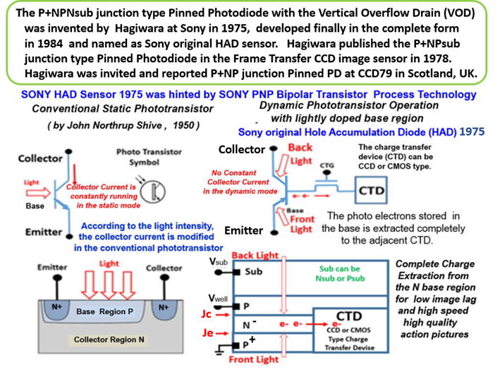
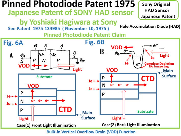
結論とまとめとして、このP+NPNsub接合型のPined Photodiodeの最大
の特徴は、暗電流の抑圧となります。これが萩原の発明の最重要点です。
萩原1975年日本国特許を参照してください。
In the conclusion and summary, the P+NPNsub junction type pinned photodiode
does not suffer the dark current problem. This is the most important
feature of this Hagiwara invention. See JAP 1975-134985 by Hagiwara.
このP+NPNsub接合型のPinned Photodiodeは次の3つの融合体です。
(1) 暗電流を抑圧した、P+NP接合型の Pinned Photodiode
(2)残像のない、完全空乏化状態の埋め込みPhotodiode
(3)さらに縦型の Overflow Drain (VOD) 機能が組み込まれた受光素子
This P+NPNsub juction Pinned Photodiode is a combination of
(1) the P+NP junction type Pinned Photodiode with low dark current,
(2) the image-lag-free complete-depletion-mode Buried Photodiode
(3) with the vertical overflow drain (VOD) function.
また萩原は日本国特許 (1975-127647 ) で、次の2つを発明ました。
(4)裏面照射型の N+NP+N 接合型 Pinned Photodiodeでもあり、
(5)表面型の電荷転送電極(CTG)をまたMOS容量型の一時的な
Buffer 記憶メモリーとしても機能させて、Global Shutter
動作モードも可能にしている受光素子構造を発明しました。
Hagiwara also proposed in the Japanese Patent JAP 1975-127647
(4) the N+NP+N junction type Pinned Photodioe
with the back light illumination scheme
(5) Surface type Charge Trasfer Gate(CTD) serving also
as the one type MOS capacitor type Buffer Memory
for Global Shutter Operation Scheme
問題はこの2つの特許をだれも理解せず、学会の論文でも一度も
引用されることがなかったことが最大の悲劇でした。
It was very sad that no one understood the details of these
Hagiwara patents, and that no one ever quoted Hagiwara patents
in their publication papers in the past. That was all tragedy.
萩原が1975年に発明出願した、特許 昭50-127647
の特許請求範囲の定義文は以下のようになっています。
(1)半導体基体(Psub)の一方の主面側に、絶縁膜を介して電荷
転送用電極(CTG)が被着配列される1の導電型(N)の転送
領域が形成され、
(2)之より上記半導体基体(Psub)の他方の主面側に上記転送
領域(N)に接する他の導電型の領域(P)と該領域に接する
1の導電型(Nwell)の領域とより成る受光領域(NPNwell
接合型受光素子)が形成され、
(3)上記転送用電極(CTG)に所要の電圧を印加することにより、
上記受光領域(NPNwell接合型受光素子)に蓄積した電荷を
上記転送領域(N)に転送し、
この時点では、信号電荷は一時的にこの転送用電極(CTG)に
蓄積されたままになっている。従ってこの転送用電極(CTG)
一時的な one time MOS capacitor 型の buffer memory
として機能し、CMOS型の電荷転送装置(CTD)では、Global
Shutter Operation Mode が可能となる。
(4)上記電荷転送用電極に上記所要の電圧とは異るクロック
電圧を印加して上記基体の上記一方の主面に沿って電荷の
転送を行うようにしたことを特徴とする固体撮像装置。
そして、最後に異なる電圧を印加して、隣接する電荷転送
装置( CCD 型 CTD でも CMOS 型 CTD でも OK ) に信号
電荷が最終的に転送されることになります。この特許の
実施例図から、この電荷転送が完全空乏化電荷転送である
ことは明らかです。従って、萩原は埋め込みPhotodiodeの
発明者でもあり、かつ、「空乏化Photodiode」の発明者
でもあります。
この萩原1975年特許の簡潔な特許請求範囲で定義された構造は
単純明解な N/P/Nwell/Psub 接合型サイリスター構造です。
この1975年の萩原出願特許は、萩原が、
(1)裏面照射型の Pinned Photodiode、埋め込み Photodiode、
そして 空乏化 Photodiode の発明者であり、かつ、
(2)MOS 容量型 one time buffer memory を使った、Global
Shutter 機能付き Pinned Photodiode
の発明者である証拠になります。
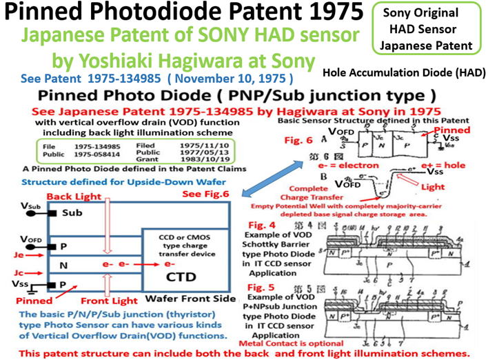
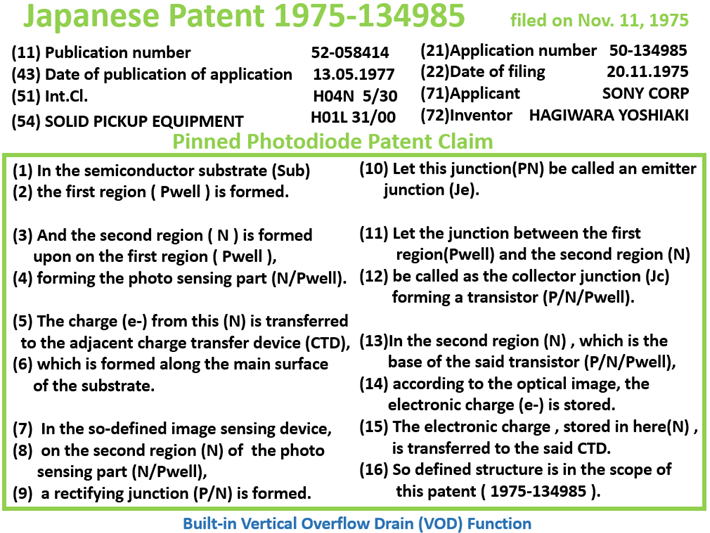
萩原が1975年に発明出願した、特許 昭50-134985
の特許請求範囲の定義文は以下のようになっています。
(1)半導体基体(Nsub) に、第1電導型の第1半導体領域(Pwell)と、
(2)之の上に形成された第2導電型の第2半導体領域(N)とが形成されて
光感知部(N/Pwell 接合受光素子)と
(3)之よりの電荷を転送する電荷転送部(CTD) とが上記半導体基体の
主面に沿う如く配置されて成る固体撮像装置に於いて、
(4)上記光感知部の上記第2半導体領域(N)に整流性接合(P+N接合)
が形成され、該接合をエミッタ接合(Je)とし、
(5)上記第1及び第2半導体領域間の接合をコレクタ接合(Jc)とする
トランジスタ( P+/N/Pwell 接合 ) を 形成し、
(6)該トランジスタのベースとなる上記第2半導体領域(N)に 光学像に
応じた電荷 を蓄積し、ここに蓄積された電荷を上記転送部(CTD)に
移行させて、その転送を行うよう にしたことを特徴とする固体
撮像装置。
特許の添付の実施例図よりこの電荷転送が完全空乏化電荷転送
であることを意味しています。すなわちこれは「空乏化Photodiode」
の発明特許でもあり、残像のない映像を提供するものです。
この最終的な受光素子構造は、P+/N/Pwell/Nsub 接合型サイリスター
構造をしており、添付の特許実施例図より縦型 overflow drain
としても機能することを明示したものです。
従って、萩原はこの特許出願により、(1) 暗電流を抑圧する、
Pinned Photodiodeの発明者であり、(2)残像のない事を特徴
とする、埋め込みPhotodode および 空乏化 Photodiodeの
発明者でもあり、かつ、(3)表面が emitter 端子となり濃い
P+層 ( Hole Accumulation 領域 )を持つ、P+/N/Pwell/Nsub
接合型サイリスター構造の様々な自由度ある付属動作のひとつ
である、縦型のoverflow drain (VOD)の発明者でもあります。
問題はこの2つの特許をだれも理解せず、学会の論文でも一度も
引用されることがなかったことが最大の悲劇でした。
It was very sad that no one understood the details of these
Hagiwara patents, and that no one ever quoted Hagiwara patents
in their publication papers in the past. That was all tragedy.
*******************************
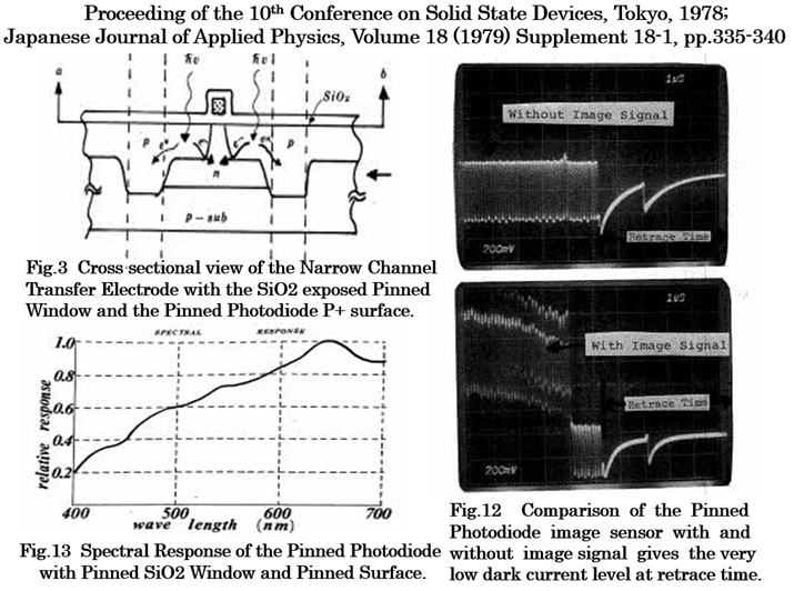
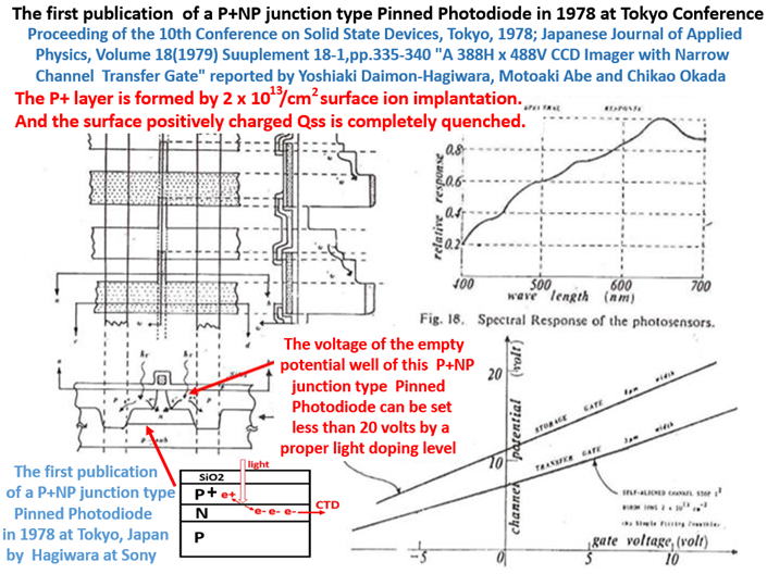
P+NP_junction_type_Pinned_Photodiode_1978_Paper_by_Hagiwara (PDF)
*******************************
●表面チャネルCCD(完全電荷転送)の電荷転送電極(CTD)を
MOS容量型Buffer Memory とした、Global Shutter 機能付きで、
かつ、裏面照射型の、Pinned Photodiode の基本特許です。
Japanese Patent 1975-127647.html
●P+NPNsub 接合型の SONY Accumulation Diode (HAD) で、
縦型Overflow Drain (VOD)機能が組み込まれた、
Pinned Photodiode (SONY HAD)の基本特許です。
Japanese Patent 1975-134985.html
****************************
*******************************
Do you know the difference of Buried and Pinned Photodiode ?
*******************************
●表面チャネルCCD(完全電荷転送)の電荷転送電極(CTD)を
MOS容量型Buffer Memory とした、Global Shutter 機能付きで、
かつ、裏面照射型の、Pinned Photodiode の基本特許です。
Japanese Patent 1975-127647.html
●P+NPNsub 接合型の SONY Accumulation Diode (HAD) で、
縦型Overflow Drain (VOD)機能が組み込まれた、
Pinned Photodiode (SONY HAD)の基本特許です。
Japanese Patent 1975-134985.html
萩原が1975年に出願した、この2件の特許と、その実施例の図のすべてが、
「萩原がその発明者である」ということの、当然ですが、確実な証拠となります。
PNP接合型または、NPN接合型の、暗電流を抑圧した Pinned Photodiode
の発明者であり、物理的構造からして、「埋め込み Photodiode 」の発明者
でもあり、また残像のない特徴を示す、「空乏化 Photodiode 」の発明者でも
あり、かつ、SONY original HAD センサーの発明者である事はになります。
****************************
****************************
Story of Pinned Photodiode( SONY HAD ) Sensor.pdf
Japanese Patent 1975-127647.html
Japanese Patent 1975-134985.html
P+NP_junction_type_Pinned_Photodiode_1978_Paper_by_Hagiwara (PDF)
****************************
Do you know the difference of Buried and Pinned Photodiode ?
****************************
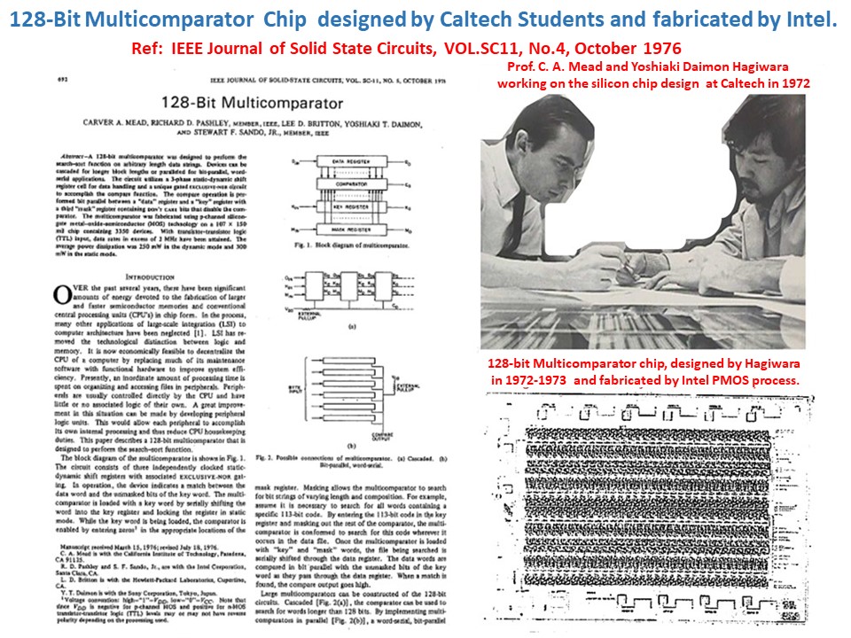
Hagiwara_Yoshiaki_CaltechDiploma_PhD1975.pdf
128_bit_Comparator.pdf
Pinned Photodiodeの発明が、NEC1980年特許を根拠に、
NECの寺西さんの発明と社会的に認知され評価されていますが
これは全くの事実誤認です。SONYの萩原の1975年特許が
先行特許で存在します。
真実はいつもひとつです。
Pinned Photodiodeの真の発明者は萩原です。
実際にSONYのHADとNECの埋め込みPhotodiodeとの
水面下の特許戦争にかかわる文書が残っています。
NEC1980年特許とSONY1975年萩原特許との間の特許戦争
NECは負けてSONYが勝ち、その結果、敵対していたNECは特許
戦争に負けてビジネスが傾く、image sesnor のビジネスから撤退
したという醜い冷酷なお金の亡者の特許戦争が裏にありました。
**********************
The AIPS image sensor watching at its inventor, Yoshiaki Hagiwara.
return to the TOP Page
**********************