*************************************************
Original Japanese Patent 1975-134985
on the P+NPNsub junction type
SONY Original Hole Accumulation Diode (HAD)
Pinned Photodiode
invented by Yoshiaki Hagiwara at Sony in 1975
See the P+NPNsub junction type Pinned Photo Diode Patent ( PDF )
*************************************************
Japanese Patent 1975-134985 by Hagiwara defines
a P+NP/Sub junction thyristor type Pinned Photodiode
with the built-in vertical oveflow drain (VOD) function.
See Japanese Patent 1975-134985 filed on Nov. 11, 1975
Visit https://www4.j-platpat.inpit.go.jp/
and type in the patent number 1975-134985
to get the original PDF patent file of
Japanese Patent 1975-134985 by Hagiwara 1975 at Sony.
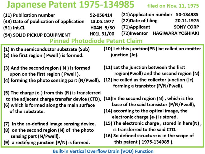
出願番号 特願昭50-134985
公開番号 特開昭52-058414
公告番号 特公昭58-046905
特許請求範囲 ( Patent Claim )
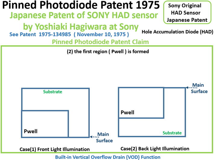
(1)半導体基体に、
(1) In the semiconductor substrate (Sub)
(2)第1導電型の第1半導体領域と、
(2) the first region ( Pwell ) is formed.
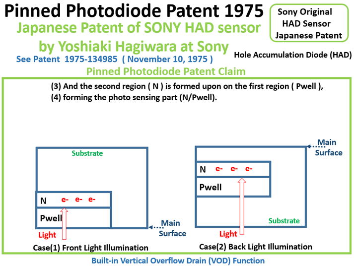
(3)之の上に形成された第2導電型の第2半導体領域とが
(3) And the second region ( N ) is formed
upon on the first region ( Pwell ),
(4)形成されて光感動部と
(4) forming the photo sensing part (N/Pwell).
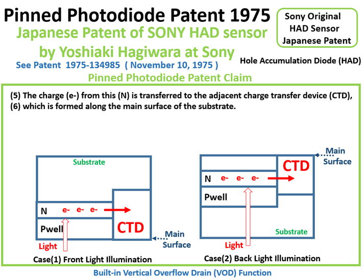
(5)之よりの電荷を転送する電荷転送部とが
(5) The charge (e-) from this (N) is transferred
to the adjacent charge transfer device (CTD),
(6)上記半導体基体の主面に沿う如く配置されて
(6) which is formed along the main surface
of the substrate.
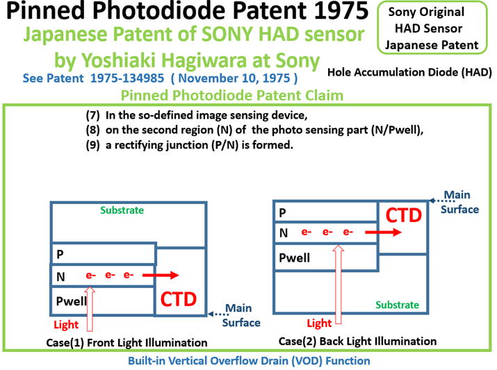
(7)成る固体撮像装置に於いて、
(7) In the so-defined image sensing device,
(8)上記光感動部の上記第2半導体領域に
(8) on the second region (N) of the photo
sensing part (N/Pwell),
(9)整流性接合が形成され、
(9) a rectifying junction (P/N) is formed.
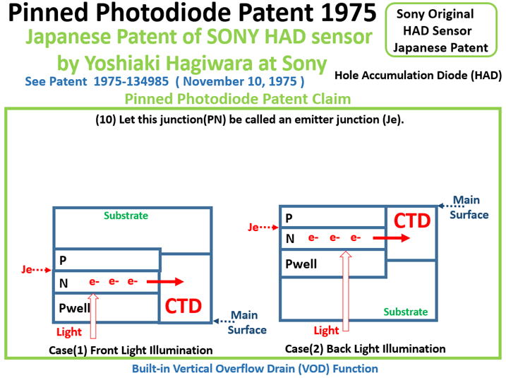
(10)該接合をエミッタ接合とし、
(10) Let this junction(PN) be called
an emitter junction (Je).
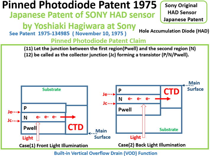
(11)上記第1及び第2半導体領域間の接合を
(11) Let the junction between the first
region(Pwell) and the second region (N)
(12) コレクタ接合とするトランジスタを形成し
(12) be called as the collector junction (Jc)
forming a transistor (P/N/Pwell).
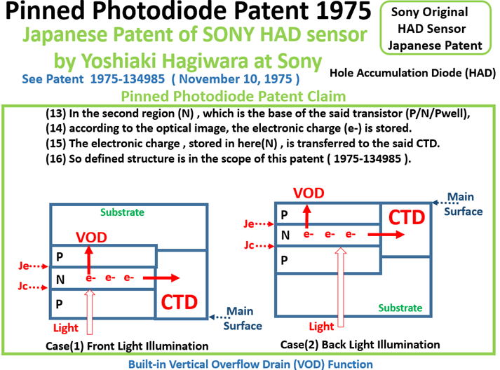
(13)該トランジスタのベースとなる上記第2半導体領域に
(13)In the second region (N) , which is the
base of the said transistor (P/N/Pwell),
(14)光学像に応じた電荷を蓄積し
(14) according to the optical image, the
electronic charge (e-) is stored.
(15)ここに蓄積された電荷を上記転送部に移行させて、
(14) according to the optical image, the
electronic charge (e-) is stored.
(16)その転送を行うようにしたことを特徴とする固体撮像装置。
(16) So defined structure is in the scope of
this patent ( 1975-134985 ).
(11) Publication number..................................52-058414
(43) Date of publication of application.........13.05.1977
(51) Int.Cl...........................................................H04N 5/30
(54) SOLID PICKUP EQUIPMENT.................H01L 31/00
(21) Application number..................................50-134985
(22) Date of filing.............................................20.11.1975
(71) Applicant...................................................SONY CORP
(72) Inventor....................................HAGIWARA YOSHIAKI
Patent Claims
(1) In the semiconductor substrate (Sub)
(1)半導体基体に、
(2) the first region ( Pwell ) is formed.
(2)第1導電型の第1半導体領域と、
(3) And the second region ( N ) is formed
upon on the first region ( Pwell ),
(4) forming the photo sensing part (N/Pwell).
(3)之の上に形成された第2導電型の第2半導体領域とが
(4)形成されて光感動部と
(5) The charge (e-) from this (N) is transferred
to the adjacent charge transfer device (CTD),
(6) which is formed along the main surface
of the substrate.
(5)之よりの電荷を転送する電荷転送部とが
(6)上記半導体基体の主面に沿う如く配置されて
(7) In the so-defined image sensing device,
(8) on the second region (N) of the photo
sensing part (N/Pwell),
(9) a rectifying junction (P/N) is formed.
(7)成る固体撮像装置に於いて、
(8)上記光感動部の上記第2半導体領域に
(9)整流性接合が形成され、
(10) Let this junction(PN) be called
an emitter junction (Je).
(10)該接合をエミッタ接合とし、
(11) Let the junction between the first
region(Pwell) and the second region (N)
(12) be called as the collector junction (Jc)
forming a transistor (P/N/Pwell).
(11)上記第1及び第2半導体領域間の接合を
(12) コレクタ接合とするトランジスタを形成し
(13)In the second region (N) , which is the
base of the said transistor (P/N/Pwell),
(14) according to the optical image, the
electronic charge (e-) is stored.
(15) The electronic charge , stored in here(N) ,
is transferred to the said CTD.
(16) So defined structure is in the scope of
this patent ( 1975-134985 ).
(13)該トランジスタのベースとなる上記第2半導体領域に
(14)光学像に応じた電荷を蓄積し
(15)ここに蓄積された電荷を上記転送部に移行させて、
(16)その転送を行うようにしたことを特徴とする固体撮像装置。
********************
Hagiwara had five important ideas in 1975
for the pinned photodiode sensor structures.
********************
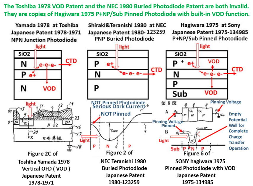
(1) Hagiwara invented P+NP/Sub junction
(thyristor) type Pinnned Photodiode
which is identical to Sony HAD Sensor
The substrate wafer can be either P-type,
N-type or intrinsic high resistivity one.
(2) Hagiwara invented the vertical overflow
drain (VOD) for the Pinnned Photodiode.
(3) Hagiwara invented the Back Light Illumination
Scheme for the Pinnned Photodiode
(4) Hagiwara invented the MOS capacitor type
Global Shutter buffer memory scheme
for the buried photodiode type Pinned Photodiode
with Back Light Illumination scheme.
(5) Hagiwara invented also the Schottky barrier
Photodiode for ILT CCD Image Sensor.
********************
Hagiwara invented the Pinned Photodiode in 1975 in his
two Japanese Patents: ( 1975-127647 and 1975-134985)
Hagiwara Patent 1975-127647 filed on Oct 22, 1975 defines
a NPN /Sub junction type Pinne Photodiode both with the
built-in Global Shutter Function of a MOS buffer memory
capacitance and also with the Back Light Illumination scheme.
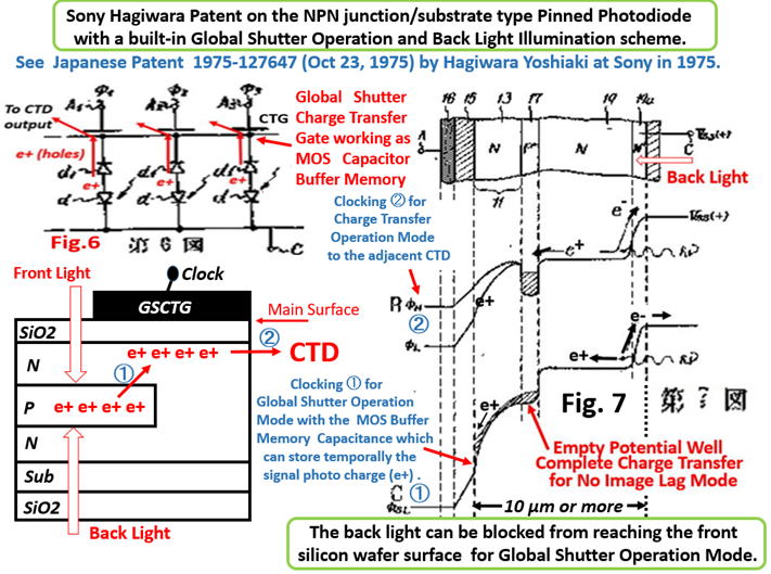
Note the difference from the normal usage of the charge transfer
gate. In this patent claim, the charge transfer gate is also used
as the short-time signal charge storage capacitance as the buffer
memory for the Global Shutter operation scheme. And later by the
second clocking the signal charge is transfered to the adjacent
charge transfer device(CTD). The CTD can be either a CCD type
CTD or a CMOS type CTD with active or passive circuits for each
pixel unit.
Hagiwara Patent 1975-134985 filed on Nov 10, 1975 defines
a P+NP/Sub junction type Pinned Photodiode with the vertical
oveflow drain (VOD) function.
One possbile future application of the Pinned Photodiode.
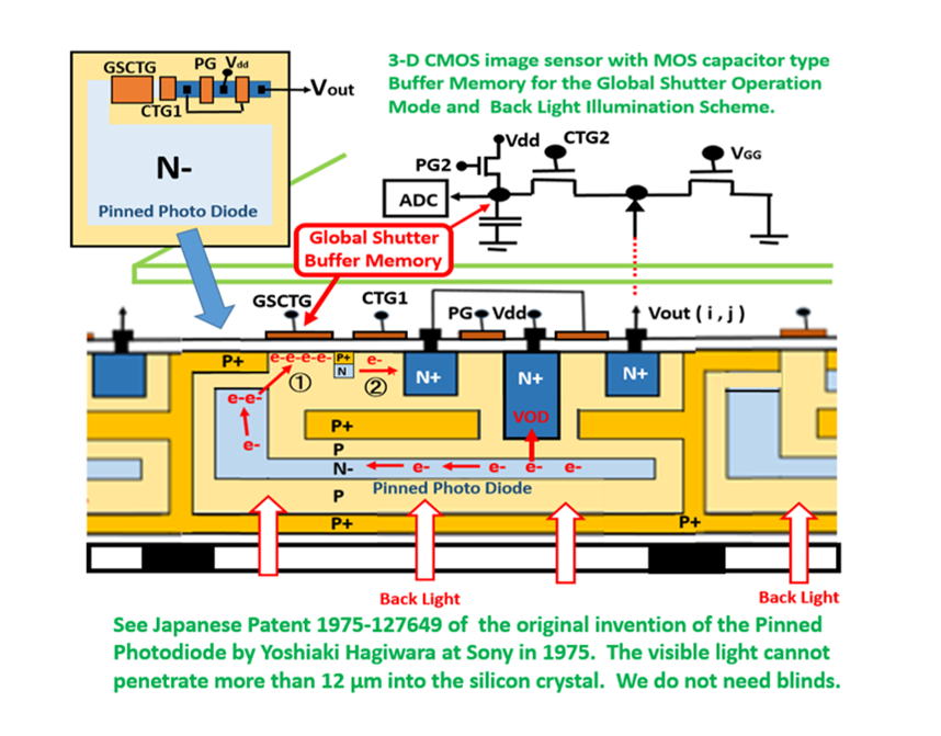
Note that there are one on-chip P+N junction pinned photodiode buffer
memory and another the second stage buffer memory capacitance for the
double global shutter operations with two reset precharge switch gates.
The very lightly doped PN- junction pinned photodiode is applied as
the photo sensing initial photodiode, and the second fairly lightly doped
PN junction pinned diode is used the first stage buffer memory floating
diffusion for the first stage global shutter scheme. Note also that there
is another second stage global shutter buffer capacitance on the
separate chip before the A/D converter circuit with another second
stage precharge reset switch gate ( Walter Kosonocky invention 1972 )
*************************************************
The AIPS image sensor watching at its inventor, Yoshiaki Hagiwara.
return to http://www.aiplab.com/TOP Page
*************************************************
*************************************************
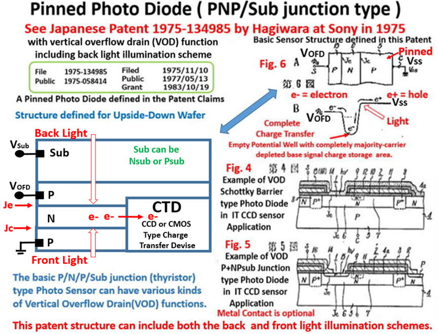
(1) The Japanese Patent 1975-134985 shown below is
the evidence that Hagiwara at Sony is the inventor of
the Pinned Photo Diode and also that Hagiwara at Sony
is the inventor of the vertical overflow drain (VOD).
(2) The Japanese Patent ( 1975-127647) shown below is
the evidence that Hagiwara at Sony is the inventor of
the Pinned Photo Diode with the Back Light Illumination.
The details are explained below.
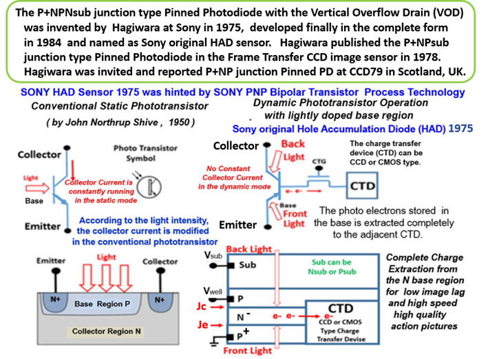
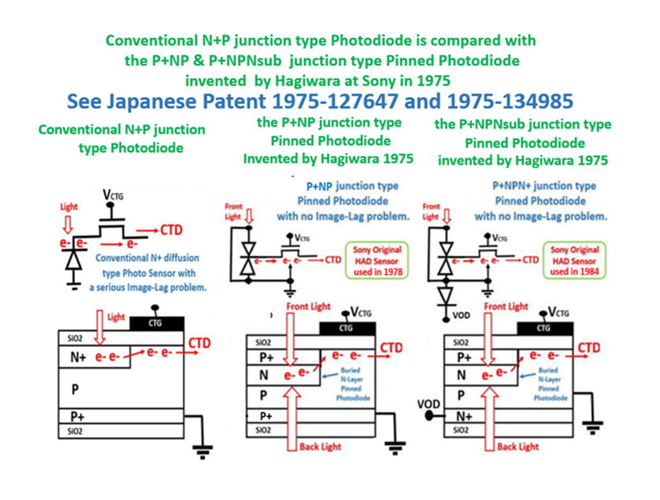
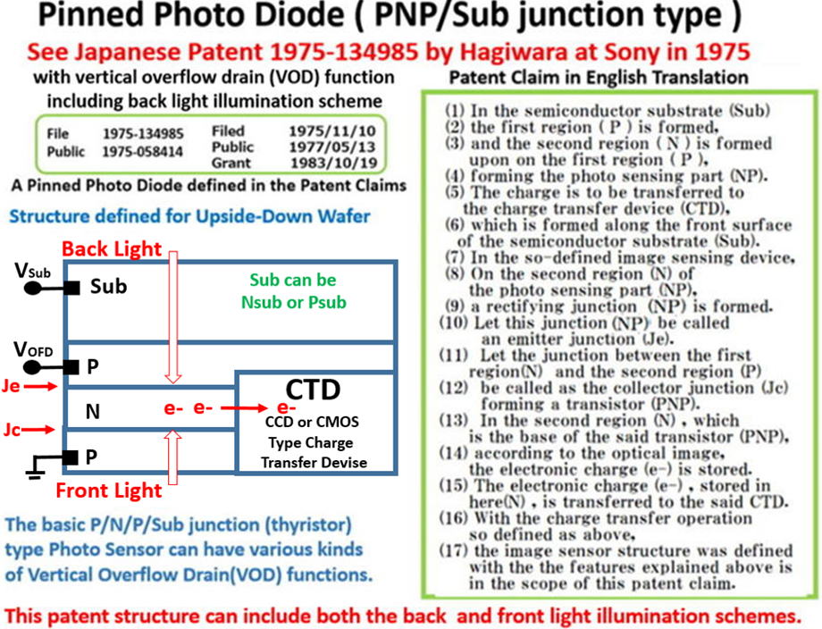
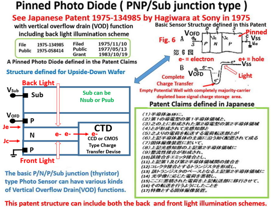
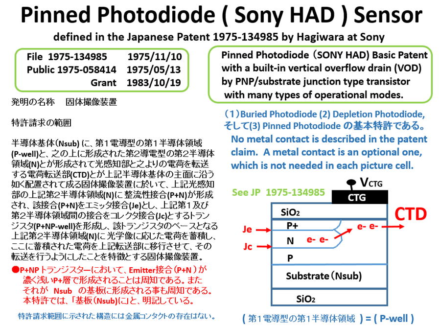
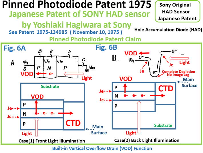
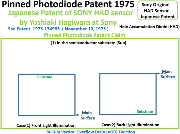
Fig.6A and Fig.6B shown below is one application example of the
structure (a) defined for Up-Side Down wafer as shown above
while Fig.4 and Fig.5 shown below are application examples of
the structure (b) defined for Up-Side Up wafer as shown above.
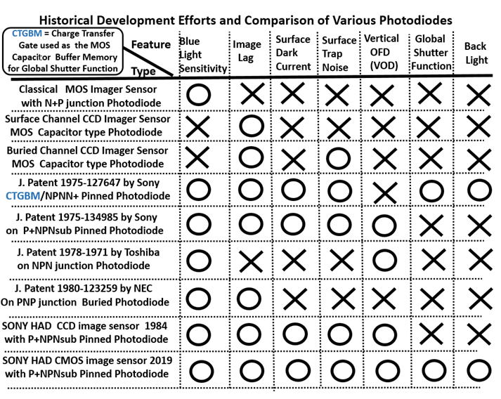
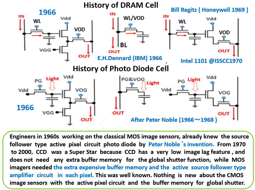
CCD was the Super Star because the global shutter function can also be buitt-in
while the conventional MOS image sensor needed an extra N+Psub diffusion
type
buffer memory capacitance which we could not afford to include in each
small pixel.
The first generation image sensor engineers all knew about this fact. It
was considered
as a weak feature of the MOS image sensor. The MOS image sensor needed
the extra
buffer memory in order to perform the golabl shutter function while the CCD image
sensor can easily perform the global shutter function without any extra
buffer memory
because the CCD itself is composed of memory capacitor arrays.
The global shutter scheme was a common understanding after CCD was invented.
And
no one tried to file a patent on this common knowledge on the MOS image
sensor unitl
more than 20 years later the CMOS process technology gets so advanced that
each
MOS image sensor pixcel can afford to include the active source follower
circuit and
the buffer memory for the global shutter function.
The Japanese Patent 1975-134985 shown above is the evidence to claim that
the Pinned Photo Diode with the vertical overflow drain (VOD) function
was
invented by Yoshiaki Hagiwara at Sony in 1975. The Japanese Patent 1975-127647
shown above is the evidence to claim also that the Pinned Photo Diode with the
vertical overflow drain (VOD) function with the back light illumination scheme was
invented by Yoshiaki Hagiwara at Sony in 1975.
************************************************
*************************************************
The AIPS image sensor watching at its inventor, Yoshiaki Hagiwara.
return to http://www.aiplab.com/TOP Page
*************************************************
Mumblings of a 70 years old man who claimes to be the inventor of the Pinned
Photo Diode
with the vertical overflow drain (VOD) function and the back light illumination
scheme.
*************************************************