**********************
The AIPS ( Artificial Intelligent Partner System ) Home Page 020
**********************
さて、冒頭での3つの基本質問の回答をここでします。
***********************************************
質問(1)
どうしてCCD image sensor が、今となっては過去になりますが、
ビデオカメラ業界ではスーパースターのように脚光を浴びる存在
だったのでしょうか?
***********************************************
Question (1)
Why was the CCD image sensor
the super star in the past ?
***********************************************
Answer :
埋め込みチャネル型のCCD の電荷転送効率は99.999% と
非常に高く、かつ、配線容量に起因するCkT 雑音は非常に低い。
The buried channel type CCD has a very high charge
transfer efficiency of 99.999% with very low CkT noise.
もう過去になりますが、昔のNTSC方式のTVシステムでは、
横の画素が720Hで、縦の画素が512Vでした。
それで、一番出力回路から遠い位置の絵素(光感知部)は、
720+512=1232回の電荷転送が最大必要となります。
In the past TV system of the 720 H x 512 V picture
resolution, we only needed the total of 1232 charge
transfers at most to transfer the signal charge from
the light detecting storage area ( the pinned photo
diode ) to the final chip output buffer circuits.
従って、最大でも、電荷転送効率が 99.999%ということは、
1回の電荷転送で 0.001 %の電荷が転送残りとなるという
ことですから、最終的に 1232回の電荷伝送では、1.232 %
の残像および混色問題が生じます。しかし、それを過去の
ビデオカメラシステムでは許容範囲としました。
Therefore, the incomplete charge transfer of
0.001 % x 1232 charge transfer gives 1.232 % of
the total incomplete charge transfer which means
only the 1.232% of image lag and color picture
contamination, which was tolerable in the past
video camera system.
かつ、配線容量による CKT 雑音が CCD image sensor の方が
当時の MOS image sensor のCKT 雑音よりはるかに小さく、
CCD image sensor の方が、当時は、 MOS image sensor より
はるかに魅力的な存在でした。
Besides, CCD image sensor has a very low CkT noise,
which is much lower than that of MOS image sensor.
***********************************************
質問(2)
どうして近年のハイビジョンのデジタルテレビ時代では、
CCD image sensor がどうして不要の存在になって
しまったのでしょうか?
***********************************************
Question (2)
Why is the CCD image sensor now obsolete
in the modern digital high vision TV era ?
***********************************************
Answer
埋め込みチャネル型CCDは CKT 雑音が たいへん小さいですが、
問題は、その電荷転送効率の値 99.999 %でした。この値では、
もはや充分な完全な電荷転送効率ではない時代になりました。
The buried channel type CCD has very low CkT noise,
but has only a limited charge transfer efficiency of
99.999%, which is now not good enough.
現在の高解像ハイビジョンTVシステムでは、たとえば,4Kテレビ
では、横3840H、縦2160V の解像度となり、出力回路に一番遠い
絵素(光感知素子=the pinned photo diode) から信号電荷を
CCDで転送するには、合計で、 3840 + 2160 = 6000 回の電荷
転送を実行する必要があります。
In the modern high resolution TV system, such as in the
4K TV system of the 3840H×2160V picture resolution,
we need the total of 6000 charge transfers at most to
transfer the signal charge from the light detecting storage
area ( the pinned photo diode ) to the final chip output
buffer circuits.
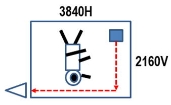
その為、転送残りは 0.001 % x 6000 = 6%にもなります。この
6%の電荷転送残りは残像にもなり、混色問題がさらに深刻となり、
より高解像で高品質画像を求めるハイビジョンTVシステムではもう
CCDは、利用価値がありません。もはや、CCDは不要な存在です。
Therefore, the incomplete charge transfer of
0.001 % x 6000 charge transfer gives 6 % of
the total incomplete charge transfer which
means the 6 % of image lag and color picture
contamination, which was not tolerable at all.
さらにCCDは大きな電極容量のかたまりであり、電荷転送時には
Clock信号を high と low を繰り返し、常に大容量を充放電する
必要があり、その充放電電流は無視できる値ではありません。
CMOSプロセスの微細化技術の進歩により、CMOS digital 回路
の消費電流が激減する中、CCDはどんどん消費電力が大きく
なります。あくまで、一時しのぎに CCD を使っていたという、
悲しい運命をたどることになりました。
Besides, the CCD image sensor consumes
a lot of electric power compared to the
very low power CMOS image sensor.
しかし、1980年当初から30年以上も世界のimage sensor の
主役として貢献してきた意味はたいへん大きなものです。今でも、
天文台などで夜空の星雲を観察する時などでは、SN比、すなわち、
信号と雑音の比が高い、超感度カメラとして活躍しています。
***********************************************
質問(3)
どうして現在、CMOS image sensorが過去の
CCD image sensor よりはるかに高性能だと
言われるようになったのでしょうか?
***********************************************
Question(3)
Why is now the CMOS image sensor dominant
over the CCD image sensor ?
*****************************************************
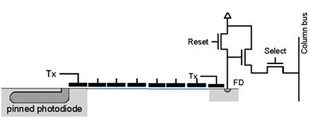
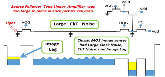
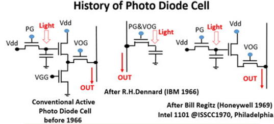
昔の古典的な MOS 型のimage sensor は one transistor 型で
その回路構成は one transistor 型の DRAM メモリセルとほぼ
同一です。もと IBM の R. H. Dennard が1966年に発明した
回路です。この回路は、その後 1969年に Honeywell社の
Bill Regits が考案発明した、信号蓄積容量に直接連結された、
プリアンプ増幅回路( 容量電圧を大電流出力に変換する回路で、
MOS transistor 型の Source follower 回路 )がついていません。
そのため、 one transistor 型は、信号増幅の手段がたいへん
難かしいものでした。Intel社はBill Regits 発明の方式を選びました。
The classical MOS image sensor was one transistor type which
was identical to the one transistor DRAM cell invented by R. H.
Dennard (IBM1966), which did not have any signal preamplifier
circuits, which was proposed by Bill Regits (Honeywell1969).
そして、この one transistor 型DRAM セルは、MOS Transistor型
の電荷転送電極 (charge transfer gate ) を介して、長くてかつ
配線容量が大きな垂直出力信号線に連結されており、その垂直
出力信号線には大きな CkT 雑音が存在し、その為、昔の古典的
な、one transistor type の MOS image sensor は CCD image
Sensor と比較してあまり魅力的ではありませんでした。
And this one transistor DRAM cell was connected directly
to the long output signal line of a very large wire capacitance,
which gave a large CkT noise. So the classical MOS image sensor
was not attractive.
DRAM セルと、 MOS Image Sensor 絵素( picture cell ) は同一です。
DRAM cell and MOS image sensor cell are identical.
MOS 型の Image Sensor の開発歴史は、
DRAM cellの開発史に順応したものです。
The history of the MOS type Image sensor followed closely
the history of the DRAM developments in the past.
One Transistor 型のDRAM Cell が IBMのR. H. Dennardにより
1969年に発明され、その後に 1969年にHoneywell社のBill Regits が
Three Transistor 型のDRAM Cell を発明しました。
今、まさに、 One Transistor 型のMOS image sensorから、1969年に
Honeywell社のBill Regits が発明した、ThreeTransistor 型の、 Active
CMOS image sensor が採用されることになりました。
これは、 Honeywell社のBill Regits の発明です。
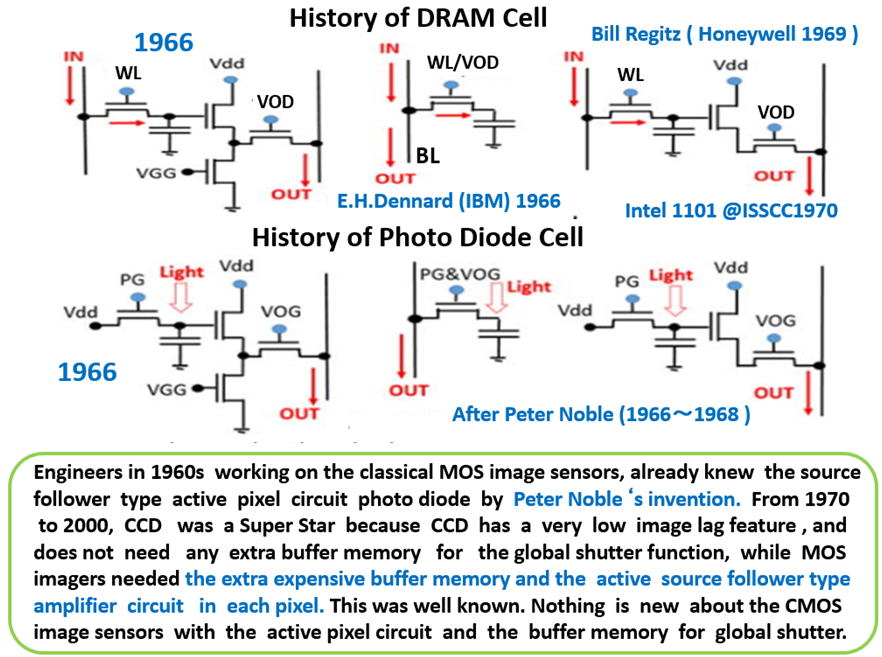
CMOSプロセス技術の微細化が進み、配線容量激減しました。かつ、
MOS transistorの物理的寸法も小さくなりました。 Honeywell 社の
Bill Regitsが 1969年に発明した、この Three Transistor型の Active
Source Follower typeの電流増幅 回路の占める面積も、光感知部、
すなわち、Pinned Photo Diode が占有する、各絵素の面積と比べて、
はるかに、占める割合が小さくなりました。
As the CMOS process scaling down technology advanced, the wire
capacitance was minimized. And also the MOS transistor size
became so small that the area occupied by the three MOS transistor
type preamplifier circuits, invented by Bill Regits ( Honeywell 1969),
could be placed at each light detecting storage area, namely at each
Pinned Photo Diode type light detecting storage area.
その結果、もはや、各絵素に、Source Follower 型の Pre Amp回路を
装備して、Active CMOS image sensor では CkT 雑音の心配は
なくなりました。光感知部 ( Pinned Photo Diode )の小さな信号電荷
の蓄積容量に蓄積された小さな信号電荷が、Source Follower MOS
Transistor の電極と直接連結されることにより、大電流を放出する
ことができるようになったわけで、配線容量のCkT雑音よりはるかに
大きな大電流が出力信号線に流れることになったためです。
The result is, we no longer suffer the CkT noise because the
preamplifier circuits can convert the small signal charge (voltage)
into a very large signal current、much larger than the CkT noise.
One Transistor 型のDRAM Cell が IBMのR. H. Dennardにより
1969年に発明され、その後に 1969年にHoneywell社のBill Regits が
Three Transistor 型のDRAM Cell を発明しました。
今、まさに、 One Transistor 型のMOS image sensorから、1969年に
Honeywell社のBill Regits が発明した、ThreeTransistor 型の、 Active
CMOS image sensor が採用されることになりました。
これは、 Honeywell社のBill Regits の発明です。
Fossum did not invented the three transitor type active CMOS image sensor.
Bill Regits (Honeywell 1969) invented the three transitor type active CMOS
image sensor. Young engineers and students in MOS image sensors in 1970s
all knew this fact, including myself as a CalTech PhD graduate student
in 1973.
,
DRAM cell and MOS image senser cell are identical.
Many MOS image sensor engineers knew the Rigitz three
transitor DRAM cell that Intel applied for Intel 1101 DRAM
chip in 1970. The active three transistor circuit for the
CMOS image sensor is the same one Rigits invented in 1969.
Fossum did not invent the active CMOS image sensor.
Hagiwara also knew the active MOS image sensor in 1975
as many other MOS image sensor and DRAM engineers did.
**************************************************************************
CMOS デジカメの開発者は Fossum ではありません。
Pinned Photo Diode の発明者は 寺西さんではありません。
しかし、事実誤認もはなはだしい事が生じ、萩原もSONYもあきれています。
**********************
これは70歳じじいのぶつぶつぼやきの独り言でした。
**********************
**********************
The AIPS image sensor watching at its inventor, Yoshiaki Hagiwara.
return to TOP Page
**********************