****************************************************
AIPS ( Artificial Intelligent Partner System ) Homepage A009
hagiwara-yoshiaki@aiplab.com
*******************************************************
Device Physics of Pinned Photodiode
*******************************************************


*******************************************************
Device Physics of Pinned Photodiode
*******************************************************
:
Let's study slowly to understand these importart figures
related to the Pinned Photodiode. More explanations
will be given below.... take your time....
(1) Introduction
***************************************************
There are a variety of photodiodes in the development history
of solid state image sensors. The most important photodiode
among them is known as Pinned Photodiode which is a P+NP
junction type photodiode with the surface layer of highly doped
P+ hole accumulation region with the buried N region used for
collection and storage of the photo signal electron charge. The
Pinned Photodiode is actually identical to SONY Hole Accumulation
Diode (SONY HAD), the same photodiode structure but with two
different names. More over the difference of the Buired Photodiode
and the Pinned Photodiode is also not well understood. They are
now being used confusingly. However, precisely speaking, the
definition of the Pinned Photodiode has an important feature
difference from the definition of the Buried Photodiode.
Pinned Photodiode has by necessity the signal charge collectiong
buried N layer, therefore, Pinned Photodiode is by necessity the
Buried Photodiode. However, the Buried Photodiode is not by
nenessity a Pinned Photodiode that has many important features
as explained below.
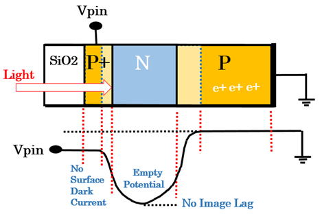
Moreover, the highly doped P+ layer of the surface hole
accumulation region in the Pinned Photodiode provides
the condition of zero surface electric field , creating a
higlhly light sensitive picture quality of a very low level
surface dark current noise.
The highly doped P+ layer, which also isolates and protects
the buried charge collecting N layer by quenching the
positively charged surface fixed charge Qss and the surface
carrier trapping interface states Nss, provides a very high
picuture quality of a vey low noise, free of 1/f trap noise.
Moreover, the signal charge, which is stored in the buied
N layer and protected by the highly P+ pinned surface
layer of surface hole accumulation, is to be transfered
to the adjacent charge transfer device (CTD) via the
charge transfer gate (CTG) by CCD like complete charge
transfer operation mode, creating a completely depleted
empty potential well in the buried N region.
Pinned Photodiode is now considered by necessity as
Depletion Photodiode which provides high quality
action pictures of low image lag. But this was not
always true in the early development of the photodiode
development efforts. See Japanese Patent 1975-127646.
The evidence that Hagiwara at SONY is the true inventor
of the Buired Photodiode will be shown in the application
example of the Japanese Patent 1975-127646 by Hagiwara
at SONY in 1975, and explained in details later below .
The Buried Photodiode is not, by necessity, the Depletion
Photodiode. The Buried Photodiode does not by necessity
have to have the signal charge to be transfered to the
adjacent charge transfer device (CTD) in the complete
charge transfer mode..
Detailes of the Depletion Photodiode is explained in
details later below.
The evidence that Hagiwara at SONY is the true inventor
of the Depletion Photodiode is also given in his Japanese
Patent 1975-127647 will be explained in details later below.
However, the Depletion Photodiode is not by necessity the
Pinned Photodiode. The Depletion Photodiode does not, by
necessity, have to have the highly doped P+ surface layer
of the hole accumulation region that provides a higlhly light
sensitive picture quality of very low surface dark current
and no 1/f trap noise.
Detailes of the Pinned Photodiode is explained in
details later below.
The evidence that Hagiwara at SONY in 1975 is the true
inventor of the Pinned Photodiode is also given in the
Japanese Patent 1975-134985 and in the Pinned Photodiode
1978 paper by Hagiwara on the P+NP junction type Pinned
Photodiode with the Pinned Window and the Pinned surface
potentail used in the 380H x 490V Frame Tranfer CCD type
charge transfer device (CTD). .
(2) Histoirical Events of Pinned Photodiode Development Efforts
*******************************************************
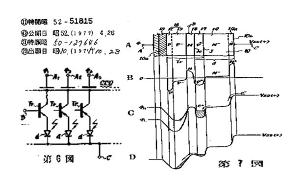
The first Buried Photodiode is proposed by Hagiwara at Sony
in 1975 in his Japanese Patent 1975-127646 in the form of
the N+N-P+NP-P junction type Buried Photodiode with the
relatively heavily doped buied charge collecting P+ layer.
See Figure 19 below, which shows the Buried Photodiode with the
P+NP junction type bipolar transistor used fas the signal charge
transfer gating (CTG). The signal charge is to be transfered to the
surface MOS capacitor which acts as a temporary buffer storage
memory for global shutter operation scheme. The application
example drawn in the Japanese Patent 1975-127646 shows a case
of back illumination scheme.
It is well known that the visible light has the wave length of 0.4 um
to 0.6 um. The blue light of the 0.4 um wave length can penetrate
only about the 0.3um depth into the silicon crystal while the red
light of the 0.6 um wave length can penetrate into the silicon crystal
upto about at the 10 um depth. Hence to cover the whole range of
the visible light, the N+N-P+ N junction type Buried Photodiode
structure was essential. That is why the N- region was drawn
relatively wide in the application example shown in the Japanese
Patent 1975-127646 . The back side has the N+N impurity doping
profile which provides the barrie for the photo signal charge (e+)
to be directed to the P+ signal charge collecting buried P+ layer.
If the silicon wafer has more than 12 um thickness, the visible
light cannot reach the front surface of the surface MOS capacitor
which can be used as the temporary buffer memory for the
global shutter operation. We do not any extra blind formation
to protect the signal stored temporarily in the surface MOS
buffer memory capacitor.
Figure 21 shows the N+NP+ junction type Buried Photodiode,
drawn in the Japanese Patent 1975-127646 ( Oct 23, 1975 )
by Hagiwara at Sony , with the P+NP-P bipolar transistor type
Charge Transfer Gating (CTG) and with P-type Buried Channel
MOS Capacitor used as the temporary storage buffer memory
for Global Shutter operation in back light illumination scheme.
The Japanese Patent 1975-127646 ( Oct 23, 1975 ) by Hagiwara
at Sony is the evidence that Hagiwara at Sony is the true inventor
of the Buired Photodiode.
Figure 19
The N+NP+ junction type Buried Photodiode, drawn in the Japanese
Patent 1975-127646 ( Oct 23, 1975 ) by Hagiwara at Sony , with the
P+NP-P bipolar transistor type Charge Transfer Gating (CTG) and
with P-type Buried Channel MOS Capacitor used as the temporary
storage buffer memory for Global Shutter operation in back light
illumination scheme.
The Buried Photodiode (BPD) itself is a simple PNP junction type
photodiode that may still have the remaining signal charge (e+) in
the charge collection region when reset.
Buried Photodiode(BPD) is not by necessity Depletion Photodiode
(DPD) that has no image lag. Moreover, Buried Photodiode (BPD)
is not by necessity Pinned Photodiode (PPD) that has no dark
current.
The surface potential of the Buired Photodiode is not by necessity
pinned. Therefore, the surface electric field and the surface fixed
positive charge +Qss may generate the undesired serious dark
current that degrades image output quality and also creates silicon
chip yield problems.
However, as seen in the drawing of Japanese Patent 1975-127646,
this is a Pinned Photodiode with the Buried P+ charge collecting
and storage region. This is Buried Photodiode and also Pinned
Photodiode.
The Pinned Photodiode is by necessity Buried Photodiode.
This Japanese patent shows an example of the Pinned Photodiode,
which is by necessity Buried Photodiode.
The Pinned Photodiode is now considered normally by necessity
Depletion Photodiode. But this is not always true.
This Japanese patent shows an example of the Pinned Photodiode,
which is not, by necessity a Depletion Photodiode.
Anyway, this picture drawn in Hagiwara 1975 Japanese Patent
1975-127646 is the clear evidence that Hagiwara at SONY is
the true inventor of the Buried Photodiode in 1975.
The application example drwan by Hagiwara at Sony in 1975
in the Japanese Patent 1975-127646 was the P+ type charge
collecting buried layer with the hole signal charge (e+) .
However, the idea can be easily extended to the case of the
N type charge collecting buried layer with the negatively
charged electron signal charge (e-) as shown below.
Figure 20
Hinted by the N+N-P+N junction type Buried Photodiode, with the
charge collecting and storage buried P+ layer, which is drawn in the
Japanese Patent 1975-127646 ( Oct 23, 1975 ) by Hagiwara at Sony,
the idea can be easily extended to the PNP junction type Buried
Photodiode with the N type charge collecting buried layer with the
negatively charged electron signal charge carrier (e-).
Moreover, hinted with this idea described in the Japanese Patent
1975-127646, described above, Hagiwara at SONY in 1975 also
filed at the same time another Japanese Patent 1975-127647 as
shown below in Figure 21.
The N+NP+ junction type Depletion Photodiode, drawn in the Japanese
Patent 1975-127647 ( Oct 23, 1975 ) by Hagiwara at Sony, with P-type
Surface Channel MOS Capacitor used as the temporary storage buffer
memory for Global Shutter operation in back light illumination scheme.
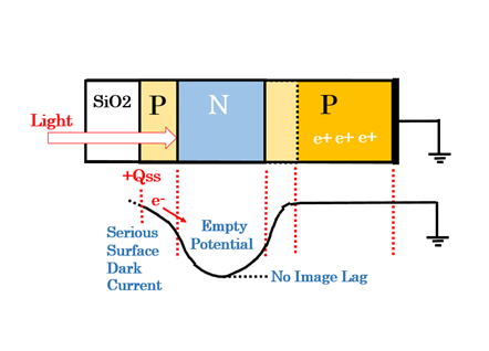
This Depletion Photodiode is also a Buried Photodiode that has a charge
collecting and storage buried P+ layer. The signal charge is completely
depleted from the N buried storage region and transfered to the adjacent
MOS bufffer memory capacitor, providing a high picture quality of the
high speed fast action picture with no image lag picture.
The Japanese Patent 1975-127647 ( Oct 23, 1975 ) by Hagiwara
at Sony is the evidence that Hagiwara at Sony is the inventor of
the Depletion Photodiode with no image lag feature by the
complete charge transfer operation mode with the completely
emplty potential well.
Figure 21
The N+NP+ junction type Depletion Photodiode, drawn in the Japanese
Patent 1975-127647 ( Oct 23, 1975 ) by Hagiwara at Sony, with P-type
Surface Channel MOS Capacitor used as the temporary storage buffer
memory for Global Shutter operation in back light illumination scheme.
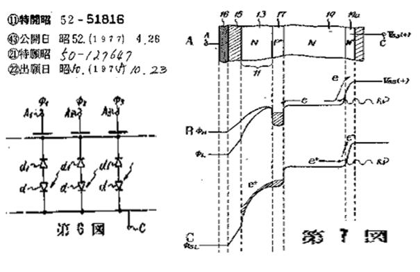
Figure 22
Hinted by the N+N-P+N junction type Depletion Photodiode, with the
charge collecting and storage buried P+ layer, which is drawn in the
Japanese Patent 1975-127647( Oct 23, 1975 ) by Hagiwara at Sony,
the idea can be easily extended to the PNP junction type Depletion
Photodiode with the N type charge collecting buried layer with the
negatively charged electron signal charge carrier (e-).
Pinned Photodiode has by necessity the signal charge collectiong
buried N layer, therefore, Pinned Photodiode is by necessity the
Buried Photodiode with the completely depleted of the signal
charge with the empty potential well when reset. The Pinned
Photodiode is now generally refered to have the Depletion
Photodiode feature of low image lag. Hence in general the
Pinned Photodiode is considered by necessity the Depletion
Photodiode. However, the Depletion Photodiode is not by
nenessity a Pinned Photodiode that has many important
features as explained below.
The highly doped P+ layer of the surface hole accumulation
region in the Pinned Photodiode provides the condition of
zero surface electric field , creating a higlhly light sensitive
picture quality of a very low level surface dark current noise.
The highly doped P+ layer, which also isolates and protects
the buried charge collecting N layer by quenching the
positively charged surface fixed charge Qss and the surface
carrier trapping interface states Nss, provides a very high
picuture quality of a vey low noise, free of 1/f trap noise.
The evidence that Hagiwara at SONY in 1975 is the true
inventor of the Pinned Photodiode is also given in the
Japanese Patent 1975-134985 and in the Pinned Photodiode
1978 paper by Hagiwara on the P+NP junction type Pinned
Photodiode with the Pinned Window and the Pinned surface
potentail used in the 380H x 490V Frame Tranfer CCD type
charge transfer device (CTD).
Figure 23
The Pinned photodiode with the heavily doped P+ surface layer,
drawn in the amplication example of the Hagiwara 1975 Japanese
Patent 1975-134985, which is used for the Buried Channel Interline
Transfer CCD image sensor.
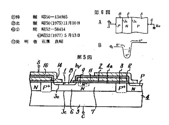
The buried N type base region in the PNP junction type photodiode
structure has the same doping level of the lightly doped buried
channel CCD, and can be completely depleted of the signal charge
to the adjacent buried channel CCD type readout charge transfer
device (CTD) by the complete charge transfer so that we have
no image lag picture. It is cleat from the application exmaple
shown in the Japanese Patent 1975-134985 that this is also
the Depletion Photodiode.
As shown in Figure 24 of the simplified P+NP junction type
Pinned Photodiode, the surface hole accumulation layer is
shown to have such a very heavily doped P+ region that can
have a fixed or Pinned potential by the external metal Ohmic
contact. The charge collecting N region is a buried N layer
under the P+ surface layer. Hence, this is also a Buried
Photodiode.Hence we conclude this is the Pinned Photodiode,
and also is Depletion Photodiode, and also is Bried Photodiode.
Hence the Pinned Photodiode is also by necessity Depletion
Photodiode with complete charge transfer operation mode.
Figure 24
The simplified P+NP junction type Pinned Photodiode structure
drawnin the Japanese Patent 1975-134985, whichi is also Depletion
Photodiode, and also is Buried Photodiode.
.
The evidence that Hagiwara at SONY in 1975 is the true
inventor of the Pinned Photodiode is also given in the
Japanese Patent 1975-134985 and in the Pinned Photodiode
1978 paper by Hagiwara on the P+NP junction type Pinned
Photodiode with the Pinned Window and the Pinned surface
potentail used in the 380H x 490V Frame Tranfer CCD type
charge transfer device (CTD). .
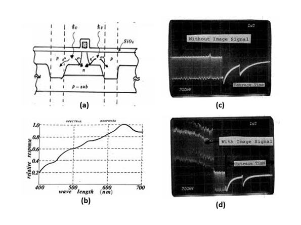
As shown in Figure 025 below, the image sensor has Pinned window
(a) with the heavily doped P+ Pinned Surface potential connected
to the substrate voltage by option with excellent blue light sensitivity.
(b). The P+NP junction type Pinned Photodiode with the self-aligned
boron atom ion implantation, forming the P+ hole accumulation
layer at the silicon surface to quench the surface dark current
as shown in the signal output wave form with no illuminated
light (c) and with illuminated light(d) .
See the Pinned Photodiode 1978 paper by Hagiwara
by Y. Daimon-Hagiwara, M. Abe, and C. Okada,
“A 380Hx488V CCD imager with narrow channel transfer
gates,” Proceedings of the 10th Conference on Solid State
Devices, Tokyo, 1978; Japanese Journalof Applied Physics ,
vol. 18, supplement 18-1, pp. 335-340, 1979.
Figure 25
The original Pinned window (a) with the heavily doped P+ Pinned
Surface potential connected to the substrate voltage by option
with excellent blue light sensitivity (b). The P+NP junction type
Pinned Photodiode with the self-aligned boron atom ion implantation,
forming the P+ hole accumulation layer at the silicon surface to
quench the surface dark current as shown in the signal output wave
form with no illuminated light (c) and with illuminated light(d) .
The patent claim of the Japanese Patent 1975-134985 actually
defined the P+NP junction bipolar transistor stucture in the
N type substrate.
Figure 26a
Conventional Phototransistor in 1948. John Northrup Shive
(February 22, 1913 - June 1, 1984) is best known for inventing this
phototransistor in 1948 ( a device that combines the sensitivity to
light of a photodiode and the current gain of a transistor ). But he also
produced experimental evidence that holes could diffuse through
bulk germanium, and not just along the surface as previously thought.
This paved the way from Bardeen and Brattain's point-contact
transistor to Shockley's more-robust junction transistor.
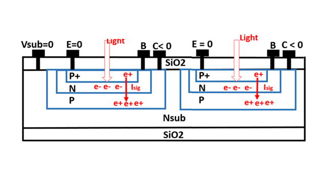
Figure 26b
Dynamic Phototransistor with Floating Base used as Signal Charge Storage
Region, the original form of the P+NPNsub junction type Pinned Photodiode
invented by Hagiwara at Sony in 1975. See Japanese Patent 1975-134985.
Figure 26c
Dynamic Phototransistor with Floating Base used as Signal Charge
Storage Region, the P+NPNsub junction type Pinned Photodiode
with the Pinned Window with the Pinned surface potentail of
the P+ hole accumulation layer pinned directly by the substrate
voltage.
This is the SONY Hole Accumulation Diode (SONY HAD) invented
by Hagiwara at Sony in 1975 in Japanese Patent 1975-134985.
See also the paper “A 380Hx488V CCD imager with narrow channel
transfer gates,” by Y. Daimon-Hagiwara, M. Abe, and C. Okada,
Proceedings of the 10th Conference on Solid State Devices, Tokyo,
1978; Japanese Journal of Applied Physics , vol. 18, supplement 18-1,
pp. 335-340, 1979.
Figure 27
The P+NPNsub junction type Thyristor structure for the light collecting
device, invented by Hagiwara in Japanese Patent 1975-134985, which is
also the P+NP junction type Pinned Photodiode (PPD), Since this is
a P+NPNsub junction type Thyristor structure which has a variety of
device operation modes that includes the Thysistor punch thru action
mode that can be applied for the vertical overflow drain (VOD) function
controlling the overflowing signal charge at the high light beam.
Figure 28
The P+NPNsub junction type Pinned Photodiode (DPD), invented
by Hagiwara in Japanese Patent 1975-134985, is also by necessity
a Depletion Photodiode (DPD) and also by necessity a Buried
Photodiode(BPD). Since this is a P+NPNsub junction type Thyristor
structure which has a variety of device operation modes that includes
the Thysistor punch thru mode that can be applied for the vertical
overflow drain (VOD).
Figure 29
The patent claim of the original Japanese Patent 1975-134985 by
Hagiwara at Sony on the P+NPNsub junction type Pinned Photodiode.
Figure 30
The patent claim in English translation of the original Japanese
Patent 1975-134985 by Hagiwara at Sony on the P+NPNsub junction
type Pinned Photodiode.
Return to AIPS HOMEPAGE TOP
(1) Electrostatic Analysis of Surface Channel MOS Capacitor Structure
*************************************************************
1.01 One Dimensional Metal/Oxide/Silicon (MOS) Structure
One dimensional metal/oxide/silicon (MOS) structure is illustrated in Fig.1.
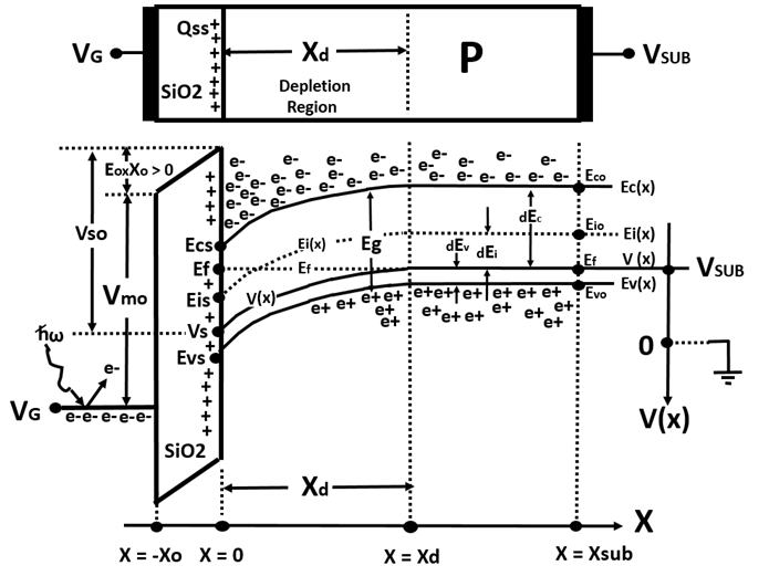
Figure 1
The band diagram of one Dimension MOS structure of
P-type silicon wafer with a positive gate voltage
The structure consists of a metallic polysilicon gate followed by a layer of
silicon dioxide of thickness Xo which rests on the P type silicon substrate
with the impurity charge density Na.
Both sides of the metal oxide semiconductor (MOS) structure are pinned
by the external voltages. One side is pinned by the gate voltage VG which
has a strong influence on the values of the surface potential Vs, the surface
electric field Es and the depth of the depletion region Xd. The other side is
also pinned by the substrate bias voltage Vsub.
The value of the Fermi energy level Ef is defined to be the reference voltage
which is equal to the substrate bias voltage level Vsub. They provide the
boundary conditions for the Poisson equation that governs the internal
potential V(x), the density n(x) of the freely moving electron fog with
the negative electronic charge e- and the density p(x) of the freely floating
bubbles with the positive electronic charge e+ of hole carriers.
The Poisson equation for this one dimensional MOS structure, which is
governing the potential energy V(x) , the free charge carrier densities N(x)
for electrons and P(x) for holes, is shown below.
d*d V(x) / dx*dx = { D(x)+N(x) - P(x) } / Dsi …… (1)
The dielectric constants are denoted as Dsi in the silicon crystal and
Dox in the oxide. The impurity doping profile D(x) inside the silicon
wafer is given as a function the depth x in the silicon wafer.
We will solve this Poisson equation numerically for an arbitrary impurity
doping profile D(x). The metal oxide work function is denoted by Vmo
and the oxide semiconductor barrier height by Vso. The total offset
voltage drop ( VG - Vs ) across the gate oxide is given by
( VG - Vs ) = ( Vmo -Vso ) + EoxXo … (2)
We also have the following relationship by the Gauss law.
( Qss - Qsig )= Dsi Es - Dox Eox ……(3)
The positive fixed interface charge Qss is present at the silicon
surface at x = 0 and the amount of the effective total negative
mobile free electrons Qsig are attracted at the silicon surface x = 0
by the positive gate voltage VG. We denote the oxide capacitance
as Co = Dox/ Xo, and define the offset gate voltage VGG and
the semiconductor metal offset voltage Vsm.
VGG = VG + Vsm …(4a)
Vsm = ( Vso - Vmo ) + ( Qss - Qsig) / Co …(4b)
From these relationships we can obtain a relationship between
the surface potential Vs and the surface electric filed Es
at the silicon surface x = 0.
Vs + Dsi Es / Co = VGG … (5)
Rewriting Eq. (5), we also get the value of the surface electric field Es
as a function of the offset gate voltage VGG and the surface potential Vs.
Es = ( Co / Dsi ) ( VGG -Vs ) ………(6)
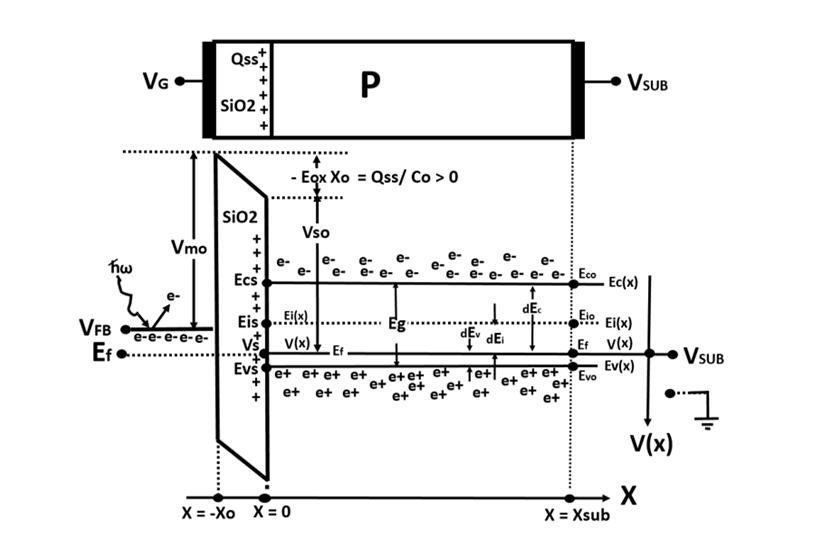
Figure 2
The band diagram of one Dimension MOS structure of
P-type silicon wafer at the flat band gate voltage.
As shown in Fig. 2, when we have a flat band condition, we have zero
surface electric field Es = 0. And at the flat band condition, the surface
potential Vs is equal to the substrate reference voltage Vsub which is
defined to be the level of the Fermi level. Hence we have Vs = Ef = Vsub.
Then, from the relationship given by Eq. (5) since we have Es =0, the
offset gate voltage VGG is equal to the surface potential Vs which is
equal to the reference Fermi energy level Ef.. That is, we have VGG = Ef.
Since the offset gate voltage VGG and the gate voltage VG are related
by Eq. (4a) and Eq. (4b), we obtain the flat band gate value VFB as shown
below.
VFB = Ef - Vsm ………(7)
When the gate voltage VG is equal to this flat band voltage VG = VFB ,
we have Es = 0 and Vs = Ef conversely. The presence of the positive fixed
charge Qss at the silicon oxide surface lowers the value of the flat band
voltage VFB as shown by Eq. (7) above with Eq. (4b).
When the gate voltage VG becomes greater than this flat band voltage VFB,
the minority carrier electrons will be attracted toward the silicon surface
and the silicon surface begins to form a channel for the mobile electrons
to flow. Historically, the understanding of the metal/Sio2 and Si/SiO2
barrier energies ( Vmo-Vso ) and the stabilizing the surface positive
fixed charge Qss played very important roles in the history of the early
PMOS and NMOS transistor integrated circuit fabrication processes.
1.02 Electron and Hole Mobile Charge Carriers at the thermal Equilibrium
At the thermal equilibrium, we have zero current density both for electron
and hole charge carriers. That is, we have Jn = 0 for electron charge carrier
density N(x) and Jp = 0 for hole charge carrier density P(x). Here we used
the Einstein relation ( μn / Dn ) = ( μp / Dp ) = ( kT/e ) .
Jn = - Dn dN(x)/dx +μn N(x) dV(x)/dx = 0 ……(8a)
Jp = - Dp dN(x)/dx -μp P(x) dV(x)/dx = 0 ……(8b)
The internal potential energy V(x) as a function of the silicon wafer
depth x is defined parallel to the band bending of the conduction energy
band edge Ec(x) , the valence band energy edge Ev(x) and the intrinsic
Fermi energy level Ei(x). And we have the following relationships with three
offset constant physical parameters, dEc, dEc and dEi defined in the
expressions shown below.
Ec (x) = V(x) - dEc = V(x) - (kT/e) ln ( Nc/No ) ……(9a)
Ev (x) = V(x) + dEv = V(x) + (kT/e) ln ( Nv/Po ) ……(9b)
Ei (x) = V(x) -dEi = V(x) - (kT/e) ln ( Ni/No ) ……(9c)
We can then express the electron and hole carrier densities N(x)
and P(x) in various ways as shown below.
N(x) = NC exp { ( Ec(x) -Ef ) / (kT/e) } ……(10a)
N(x) = Ni exp { ( Ei(x) - Ef ) / (kT/e) } ……(10b)
N(x) = No exp { ( V(x) - Ef ) / (kT/e) } ……(10c)
P(x) = NV exp { ( Ef - Ev(x) ) / (kT/e) } ……(11a)
P(x) = Ni exp { ( Ef - Ei(x) ) / (kT/e) } ……(11b)
P(x) = Po exp { ( Ef - V(x) ) / (kT/e) } ……(11c)
From these equations shown above, after some manipulations,
we get the basic relationships.
NoPo = Ni2 = NvNc exp {-Eg / (kT/e) } ……(12)
Ei(x) = (1/2) { Ec(x) + Ev(x) + (kT/e) ln ( Nc/Nv) } ………(13)
From the charge neutrality condition deep in the bulk
at the thermal equilibrium, we have
Po = Na + No. …… (14)
we obtain the values of the carrier densities No and Po
in the bulk at the thermal equilibrium in terms of the
uniform doping level Na and the intrinsic carrier density Ni.
Po = (1/2) { Na + sqrt ( Na2 + 4 Ni2 ) } ……(15a)
No = 2 Ni2 / { Na + sqrt ( Na2 + 4 Ni2 ) } ……(15b)
Figure 1
The band diagram of one Dimension MOS structure of
P-type silicon wafer with a positive gate voltage
As illustrated in Fig. 1, the values of the conduction band
energy edge Ec(x), the intrinsic Fermi level Ei(x) and the
conduction band edge Ev(x) at the silicon surface x = 0 are
denoted here respectively as Ecs = Ec(0), Eis = Ei(0) and
Evs = Ev(x) while at the silicon bulk deep in the substrate
at x = Xsub they are denoted as Eco = Ec ( Xsub ),
Eio = Ei ( Xsub ) and Evo = Ev ( Xsub ) respectively.
The surface potential at x =0 is denoted as Vs = V(0).
In the bulk, we have V(x) = Ef. Since in the bulk we have P(x)=Po
and N(x)=No. We also have the following relationships in the bulk.
No = NC exp { ( Eco-Ef ) / (kT/e) } ……(16a)
No = Ni exp { ( Eio - Ef ) / (kT/e) } ……(16b)
Po = NV exp { ( Ef - Evo ) / (kT/e) } ……(16c)
Po = Ni exp { ( Ef -Eio ) / (kT/e) } ……(16d)
( Eco - Ef ) = (kT/e) ln ( No /NC ) ……(17a)
( Eio - Ef ) = (kT/e) ln ( No /Ni ) ……(17b)
( Ef - Evo ) = (kT/e) ln ( Po /NV) ……(17c)
( Ef - Eio ) = (kT/e) ln ( Po /Ni) ……(17d)
As we increase the substrate impurity concentration Na, the hole
carrier density Po in the bulk in the thermal equilibrium also
increases. Normally the ratio Nv / Po is greater than 1 but
approaches to 1 as the value of Na, and hence Po also, gets
closer to the value of the effective carrier density Nv.
In the degenerate semiconductor, the ratio Nv/Po approaches
to 1. Therefore as we increase the wafer doping level Na
furthermore, eventually we will have the degenerate P+ silicon
wafer with the valence band edge Evo in the bulk equal to
the Fermi level Ef . That is, we will have Evo = Ef in the bulk.
From the relationship Eq. (12) in this degenerate P+ silicon
wafer, with the condition Po = Nv and Evo = Ef , we conclude
dEc = Eg which gives Eco = Ef - Eg.
At the same time, we will also have that the internal voltage V(x)
gets very close to the valence band edge Ev(x). And for the
degenerate P+ semiconductor, we have V(x) = Ev(x) throughout
inside the silicon wafer
1.03 Strong Inversion Condition
The strong inversion condition is defined as N(0) = Po , that is,
when the minority electron density N(x) at the silicon surface x=0
is equal to the density Po of the majority carrier in the bulk
at the thermal equilibrium. The threshold voltage Vth is defined
to be the gate voltage VG which creates this strong inversion
condition, N(0) = Po.
At this condition, the silicon surface becomes conductive and
creates a channel for the electric current to flow. When this
MOS capacitor is used as the gate structure of a MOS transistor,
the threshold voltage Vth is also called as the turn on voltage
to create a channel under the MOS gate for the electron current
to flow.
The strong inversion condition is defined at N(0) = Po.
Hence we also have the following relationships at the strong
inversion condition.
Po = NC exp { ( Ecs -Ef ) / (kT/e) } ……(18a)
Po = Ni exp { ( Eis - Ef ) / (kT/e) } ……(18b)
Po = No exp { ( Vs - Ef ) / (kT/e) } ……(18c)
The threshold gate voltage Vth is defined to be the gate voltage
VG that turns on the strong inversion condition when the minority
carrier electron density N(x) at the silicon surface x= 0 becomes
the bulk majority carrier density Po.
That is, at this gate voltage VG = Vth, the surface electron carrier
density becomes equal to the substrate doping level N(0) = Po.
We obtain the total band bending ( Vs - Ef )
at the onset of the strong inversion from Eq. (18c) as
( Vs - Ef ) = (kT/e) ln( Po / No ) ……(19)
Here we define the physical parameter VB to be one half of
the total band bending ( Vs - Ef ) at the onset of the strong
inversion. From Eq. (12), we then have the following relationships.
2VB = ( Vs - Ef ) = (kT/e) ln( Po / No ) ……(20a)
VB = ( kT / e ) ln( Ni / No ) = ( kT / e ) ln( Po / Ni ) ……(20b)
Writing the intrinsic fermi level at the surface x = 0 as Eis = Ei(x),
at the turn on gate voltage VG =Vth with the condition N(x) = Po
at the surface x = 0, from Eq. (18b) we obtain
Eis = Ef + ( kT / e ) ln( Po / Ni ) ……(21a)
And in the bulk by writing Eio = Ei ( Xsub ) from Eq. (16b) we obtain
Eio = Ef -( kT/e ) ln ( Ni/No ) ……(21b)
Then, from Eq. (21a) and Eq. (21b) we have
VB = ( Ef - Eio ) = ( Eis - Ef ) ……(21c)
At this strong inversion turn on gate voltage Vth, with the internal
voltage V(x) axis defined downward for the negatively charge electron
carriers, the intrinsic Fermi level Eio at the bulk will be above the Fermi
level Ef by the amount ( Ef - Eio ) = VB > 0 as much as the intrinsic
Fermi level Eis at the silicon surface is below the intrinsic Fermi level Ef,
by the amount ( Eis - Ef ) = VB > 0.
1.04 Depletion Approximation
By depletion approximation, inside the depletion region, by assuming
n(x) = p(x) = 0 and D(x) = Na and the boundary conditions V(x) = Vs
at x =0 and V(x) = 0 at x = Xd, we can express the internal voltage V(x)
as a function of the position x shown below.
V(x) = Ef -( Na/2Dsi ) ( Xd - x )**2 ………(22a)
V(x) = Vs -Es x + ( Na/2Dsi ) x** 2 ………(22b)
And the electric field E(x)= - dV(x)/dx inside the depletion region
can be expressed as
E(x) = ( Na/Dsi ) ( Xd - x ) ………(23a)
E(x) = Es- ( Na/Dsi ) x ………(23b)
At the edge x = Xd, of the depletion region,
we have the conditions V(x) = Ef = Vsub
and E(x) = 0 while at the silicon surface x = 0,
we have V(x) = Vs and E(x) = Es.
Then we obtain the following relationships
between the total band bending (Vs-Ef)
and the surface electric field Es.
Vs - Ef = NaXd**2 / 2Dsi ……(24a)
Es = NaXd / Dsi ……(24b)
Vs - Ef = DsiEs**2/2Na ……(24c)
Using the relation given by Eq. (5) and Eq. (24b),
the depletion depth Xd can be expressed as a function
of the surface potential Vs and the offset gate voltage
VGG as shown below,.
Xd = ( Co / Na )( VGG - Vs ) … (25)
By introducing the physical parameters
VA = DsiNa/Co**2,
we can now obtain the value of the offset gate
voltage (VGG - Ef ) as a function of the surface
potential ( Vs -Ef ) from the relationship below.
( VGG - Vs ) = sqrt { 2 ( Vs - Ef ) VA } … (26)
At the onset of the turn on gate voltage VG=Vth, we have
( Vs - Ef ) = 2 VB … (27)
We then have at the onset of the turn on gate voltage VG=Vth,
( VGG - Ef ) = 2 VB + 2 sqrt ( VA VB ) … (28)
Then from the relationship Eq. (4a) we have
the value of the threshold voltage Vth.
Vth = Ef - Vmo+2 VB + 2 sqrt ( VA VB ) ….. (29)
Conversely, although the mathematical derivation
is not simple, we can also obtain the surface
potential ( Vs - Ef ) as a function of the offset
gate voltage (VGG - Ef ).
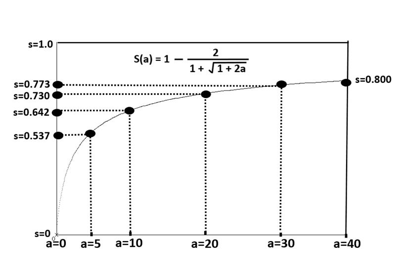
Figure 3
The values of the function S = S(a) plotted against
the input physical parameter a = VGG/VA.
We use the function S(a) shown in Fig. 3 and defined
by the following relationships with the parameter a.
a = ( VGG - Ef ) / VA … (30a)
S(a) = 1 -2 / { 1 + sqrt ( 1 + 2a) } … (30b)
( Vs -Ef ) = VA S(a) … (30c)
The value of the function S(a) increases monotonically as the input
variable a increases. However, the value S(a) is always less than 1,
but very slowly approaching to 1.
To obtain some feelings for these relationships, we now put some values
for the salient physical parameters involved in the MOS capacitor structure
under consideration.
Here we choose the substrate doping level Na=500 e /μm3 with the oxide
thickness Xo = 0.13 μm.
The dielectric constant of the silicon dioxide is Dox = 216 eV/μm
while the dielectric constant of the silicon crystal is Dox = 648 eV /μm.
We have then the oxide capacitance of Co = Dox/Xo = 1662 e/voltμm2.
The value of the parameter VA is given as VA = DsiNa/Co2 = 0.117361 V.
The effective conduction band electron density Nc = 2.8 x 10⁷ e /μm3 and
the effective valence band hole density Nv = 1.04 x 10⁷ e /μm3 are used
with the silicon energy gap of Eg = 1.082 V, to obtain the intrinsic carrier
concentration of Ni = 0.0145 e /μm3 by the relationship Eq. (12).
The value of the bulk majority carrier concentration Po obtained by Eq. (15a),
is greater than the impurity doping level Na=500 e /μm3 slightly but is very
close to Na.
We have the minority carrier electron density of No = 4.19 x 10⁻⁷ e /μm3 <<Na
in the deep bulk substrate at the thermal equilibrium from Eq. (15b).
Then, Eq. (20a) gives the total bending 2VB = 0.541316 V at the onset of the
strong inversion. We then obtain the depletion depth Xd = 1.184522 μm by Eq. (25).
And subsequently we obtain by Eq. (24b) the surface electric field of Es = 0.913983 V/μm.
Eq. (3) gives the oxide electric field Eox =2.741949 V/μm.
Using (Vso-Vmo ) = (4.45-3.20) = 1.15 eV (1) with the relationship Eq. (27)
at the onset of the strong inversion, we get ( Vth - Ef ) =- 0.252230 V from Eq. (29).
If we let the gate voltage ( VG - Ef ) = -0.252230 V,
we have VGG = 0.897770 V from Eq. (4a) conversely
with Vsm= (Vso - Vmo ) = (4.45 - 3.20) = 1.15 eV .
See Ref(1) below.
And then the value of a = VGG/VA = 7.649636 gives S(a) = 0.602957.
We get ( Vs-Ef ) = VGG S(a) = 0.541316 V by Eq. (30c) in return as before.
We get the total band bending of ( Vs - Ef ) =2 VB =0.541316 V.
We also confirm the value of VGG = 0.897770 V with the surface
potential ( Vs - Ef ) =0.541316 V and the surface electric field
of Es = 0.913983 V/μm from Eq. (5).
The potential curve V(x) as a function of the silicon depth x is plotted
in Fig. 4 by the depletion approximation is compared with the curve
obtained by the exact numerical computation.
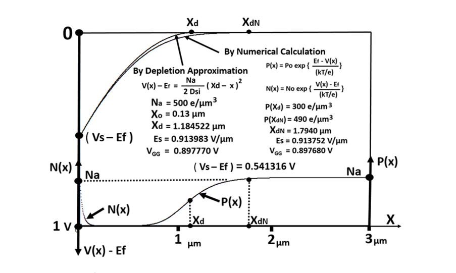
Figure 4
The internal potential V(x) and the mobile electron and
hole densities P(x) and N(x) at the onset of the strong
inversion condition.
We observe that the majority carrier hole density P(x) is nonzero
and gradually increasing in the depletion region, and has the value
of P(Xd) = 300 e/μm3, at the depletion depth Xd = 1.1845 μm.
The electric field exits in the deep depletion region in both case.
However, the actual depletion depth calculated by the numerical calculation
is Xdn = 1.7940 μm which is much deeper than the depletion approximation
depth Xd.
The actual value Xdn = 1.7940 μm, is defined at the condition
of P(Xdn) = 490 e/μm3, where the majority carrier hole density P(x)
began to reach about 98% of the bulk majority carrier density of 500 e/μm3.
1.05 Surface and Bulk Dark Current Generation
The generation of the surface dark current will give a bad picture quality
if this MOS capacitor structure is used as a light detecting device.
The surface current generation rate Gsurface(x) and the bulk current
generation rate Gbulk(x) are respectively given below.
Gsurface (x) = ( So / 2Ni ) { Ni2 -P(x) N(x) } … (31a)
Gbulk (x) = { Ni2 - P(x) N(x) }/ ( 2 Niτ) … (31b)
Here So is the surface recombination velocity which has the value
of about So = 5 x 10**7 μm/sec. And the value of the bulk recombination
timeτis about τ= 10**-7 sec. At the silicon surface under the strong
electric field the carriers are completely depleted, and we have N(x) = P(x) = 0.
And with the value of the intrinsic carrier density Ni = 0.0145 e /μm3 we have
the surface generation rate of Gsurface = So Ni / 2 = 3.625 x 10⁵ e / sec・μm2 .
With 1/60 sec integration time and the light detecting unit window area of 1μm2
we have the surface dark current of 6042 electrons, which is too large to be ignored.
We also obtain the bulk generation rate Gbulk = Ni / 2τ= 7.25 x 10**4 e / sec・μm3.
And the 1/60 sec integration time with the unit space volume of 1 μm3 of the
depletion region gives the bulk dark current of 1208 electrons which is less than
the surface dark current but still very large to be ignored.
As long as we use the MOS capacitor type light detecting device, we cannot
avoid the large surface dark current.
However, we can reduce the bulk dark current by reducing the effective
volume of the space depletion region if we form properly a heavily doped
buried P+ layer by deep high energy ion implantation as shown in the Fig.
5
below since we can reduce the volume of the space depletion region by
decreasing the depth Xd of the depletion region.
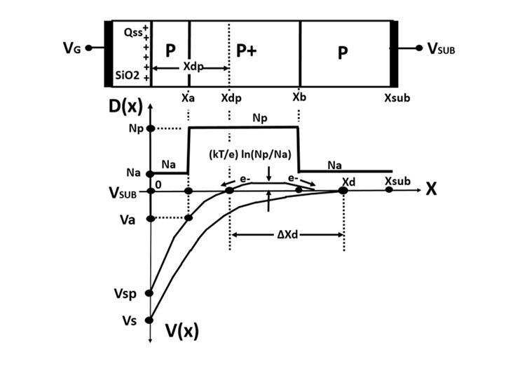
Figure 5
The impurity doping profile D(x) for the heavily doped
buried P+ layer and the internal potential V(x)
The heavily doped buried P+ layer can terminate the electric field in the
depletion region and the depth of the depletion region becomes shallower,
resulting a smaller volume of the depletion space region that gives a smaller
value for the bulk dark current.
Once the value of the surface potential Vs is known,
the depletion depth Xd for the uniform doping case
can be calculated and is given as Xd = ( Co / Na )( VGG - Vs ).
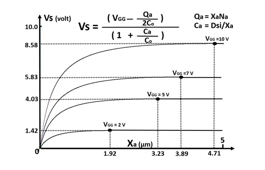
Figure 6
The surface potential plotted against the depth Xa of the buried P+ layer
with the offset gate volatge VGG as the parameter.
If we form properly a heavily doped buried P+ layer as shown in the Fig.
6
we can still have the same turn on thresh hold voltage Vth by choosing properly
the depth Xa of the buried P+ layer. However, we can reduce the depth Xd of
the depletion region as
Xd = { 1 - ( Na / Np ) } Xa + (Co/Np) ( VGG -Vsp ) … (32)
And the surface potential Vs now is given below.
VGG - Vs = WA{ sqrt ( 1 + 2 WGG / WA **2 )- 1 } … (33)
Here we defined the parameters, WA = Vp + b Vq and WGG= 2 VpVGG + b Vq**2
with b = (Np/Na) - 1, Vp = DsiNp/Co**2, and Vq =XpNp/Co.
Here we now have a new value Vs for the surface potential.
Note that if we set Np = Na, we have the same surface potential Vs and
the depletion depth Xd as before in the uniform doping case.
Note that if we set Np =Na, we have b=0 and WGG/WA**2 =VGG/VA.
Then, we return to the uniform doping case.
In the extreme case when the buried P+ layer is very heavily doped,
we have the boundary condition V(x) = Vsub at X=Xp, since the potential
of the buried P+ layer will be fixed or pinned by the substrate voltage Vsub.
The internal potential profile Vg(x) and the majority carrier hole
density Pg(x) for the case of Gaussian Buried P+ Layer are shown
in comparison with the Uniform Doping Profile case
We can obtain the surface potential Vs as a function of the depth Xp of
the buried P+ layer with the offset gate voltage VGG as a parameter
as shown in Fig. 6.
Vs = ( VGG - Qa / 2 Co ) / ( 1 + Ca / Co ) … (34)
Here we defined the parameters Qa = NaXa and Ca=Dsi/Xa.
Figure 6
The surface potential plotted against the depth Xa of the buried P+ layer
with the offset gate volatge VGG as the parameter.
If the value of Xa is larger than the depletion width Xd of the uniform
doping case, we have no change in the value of the surface potential Vs.
However, as we increase the gate voltage at the point where the depletion
depth Xd reaches the depth Xa of the buried P+ layer, the depletion will be
expanded slowly into the highly doped P+ layer region.
The signal electron charge Qsig that we can handle in this MOS capacitor
is proportional to the surface voltage difference created by the gate voltage
swing VGG. As can be inferred from Fig. 6, if we set the depth of the
buried P+ layer to be about Xa = 2μm, we still can handle about the same
amount of the signal charge Qsig that we would obtain for the uniform
doping case. This means we can reduce the depletion depth down to 40 %.
Since we had the bulk dark current 1208 e/μm3 for our case study, this
means in our rough estimation that the depletion depth of Xd=4.71μm
gives the dark current of 5690 e/μm2 while the depletion depth of
Xd=1.92 μm can reduce the dark current down to the value of 2319 e/μm2 .
For this MOS structure to be applied as an efficient MOS capacitor type
light detecting device, the doping level D(x) at the vicinity of the silicon
surface around x = 0 may be adjusted. The impurity doping profile D(x)
can be a Gaussian in particular when the process is defined to have a P
type well formation with the Gaussian hole carrier rich profile peaked
at x = Xp , which prevents the bulk dark current from the deep silicon
substrate reaching the silicon surface charge collection layer at x = 0 .
D(x) = Na + (Np -Na) exp { - ( x- Xp )**2 / Rp**2 } ………(35)
The potential curve V(x) obtained by the depletion approximation is
compared with the numerical calculation at the onset of the strong
inversion. For the Gaussian doping profile D(x) , Fig. 7 shows the
electron potential curve Vq(x) for our case study with the offset gate
voltage VGG of 10 V, the peak impurity doping level of Np = 10000 e /μm3
at the position Xp = 2μm with the spreading tail factor of Rp = 0.3μm.
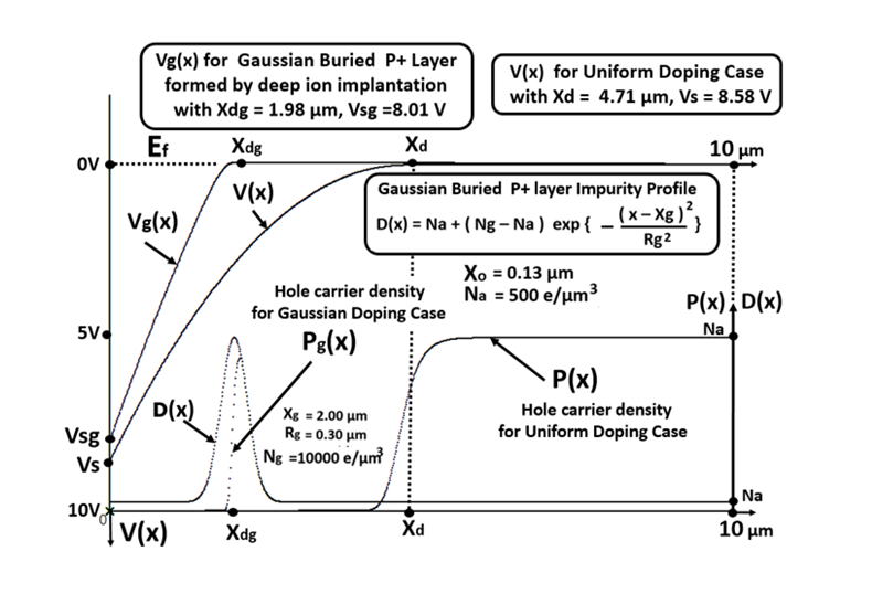
Figure 7
The internal potential profile Vg(x) and the majority carrier hole
density Pg(x) for the case of Gaussian Buried P+ Layer are shown
in comparison with the Uniform Doping Profile case
At this gate turn on threshold voltage condition N(0) = Po , since both the
depletion approximation and the exact numerical calculation must satisfy
the same boundary conditions at the surface x = 0, we must obtain
the same value for the surface potential Vs = 0.541 V in both calculation
methods.
We impose the same value for the surface potential ( Vs - Ef ) = 0.541 V
but we have slightly different values for VGG and the electric filed Es
at the condition of the strong inversion condition N(0)=Po.
By forming the heavily doped Gaussian P+ buried layer, we can have
a smaller space volume of the bulk space depletion region and the bulk dark
current is lowered because the bulk dark current is proportional to
the depletion space volume. However, we still can keep the surface
doping level D(0) as low as the substrate doping level Na. And we can
perform the strong inversion operation mode almost in the same manner
as in the uniform doping wafer case. This buried P+ layer formed by the
high energy deep ion implantation technique was the savior of the image
sensor production engineers in the early history of image sensor developments.
(2) Electrostatic Analysis of Buried Channel MOS Capacitor Structure
2.01 Buried Channel MOS Capacitor Structure with the flat band gate voltage
The one dimensional geometric structure for a buried N type channel charge
couple device is illustrated in Fig. 8 with the flat band gate voltage VG = VFB
at the thermal equilibrium condition.
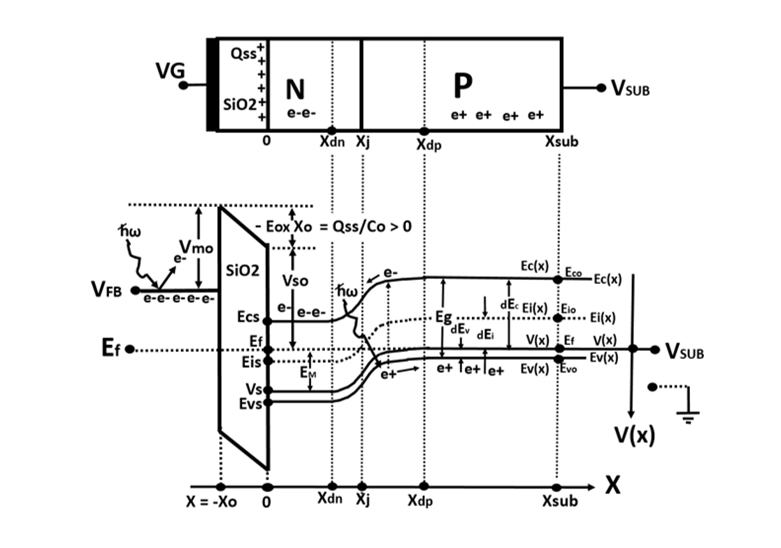
Figure 8
The NP junction type Buried Channel MOS Capacitor Structure
with the flat band gate voltage
The structure consists of a metallic polysilicon gate
followed by a layer of silicon dioxide of thickness Xo
which rests on the bulk silicon wafer with the doping
level of Na with the N type buried channel layer of
the impurity doping level of Nd for mobile electron
charge carriers e- to move around freely near the
surface.
The potential energy V(x) is define as before
with the Fermi level at the P type bulk substrate
as the reference voltage.
Near the silicon surface at the thermal equilibrium,
the electron carrier density is equal to the doping
level Nd of the buried N layer and we have the
following relationship.
Nd = No exp { ( Vs-Ef ) / (kT/e) } ……(36)
Since we also have PoNo = Ni2, and with Po being almost equal to Na, we obtain
the expression for the built-in potential VB of the PN junction.
( Vs - Ef )=VB = ( kT / e ) ln ( Na Nd / Ni2 ) …… (37)
At this value, the band at the surface is flat, and the flat band voltage is given by
VFB = ( kT / e ) ln ( Na Nd / Ni2 ) + Vms …… (38)
2.02 Buried Channel MOS Capacitor at the dynamic operation mode
Fig.9 shows the electrostatic potential V(x) of the buried channel MOS capacitor at
the dynamic operation mode when the buried channel layer is completely depleted
of the majority carrier electrons.
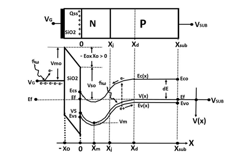
Figure 9
The NP junction type Buried Channel MOS Capacitor Structure
at the dynamic operation mode when the buried channel layer
is completely depleted of the majority carrier electrons.
Since the potential gradient dV(x)/dx > 0 at the silicon
water surface x =0 in this case, we have the following
relationship from the Gauss law,
Qss = -Dsi Es + Dox Eox …… (39)
We also have the relationship
VG = Vs - Vso - XoEox + Vmo …… (40)
We define, similarly as before, the offset voltage VGG as below.
VGG = VG - ( Vmo -Vso ) + Qss / Co …… (41)
Then we obtain the boundary condition at the silicon surface as before.
Vs + Dsi Es / Co = VGG …… (42)
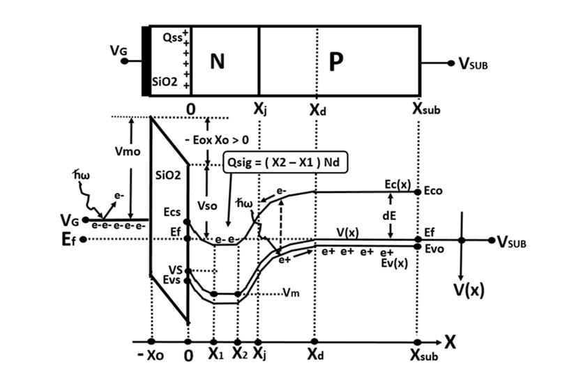
Figure 10
The NP junction type Buried Channel MOS Capacitor Structure
at the dynamic operation mode with the majority carrier mobile
electrons present in the buried channel layer.
In the more general case as described in Fig. 10 we consider the majority
carrier mobile signal electrons Qsig present in the buried channel layer,
which is given as
Qsig = ( X2 -X1 ) Nd, …… (43)
We can express by depletion approximation the minimum potential Vm and
the depletion edges, X1, X2 and Xd in terms of the signal charge Qsig and
the offset gate voltage VGG. The internal potential function V(x) is given as below.
V(x) = Vm - ( X1 - x )2 Nd / 2 Dsi for x in [ 0, X1 ] …… (44c)
V(x) = Vm for x in [X1, X2 ] …… (44b)
V(x) = Vm - ( x - X2 )2 Nd / 2 Dsi for x in [X2, Xj ] …… (44c)
V(x) = Ef + ( Xd - x )2 Nd / 2 Dsi for x in [Xj, Xd] …… (44d)
V(x) = Ef for Xd < x …… (44e)
Since we have V(x) = Vs at the silicon surface x = 0 and the internal
potential V(x) and its gradient dV(x)/dx are continuous inside the silicon
wafer, we have the following relationships.
Vs = Vm - Nd X12 / 2 Dsi …… (45)
Es = Nd X1 / Dsi …… (46)
Vm - ( Xj - X2 )2 Nd / 2 Dsi = Ef + ( Xd - Xj )2 Nd / 2 Dsi …… (47)
( Xj - X2 ) Na = ( Xd - Xj ) Nd …… (48)
Although the computation is very cumbersome, we can calculate,
the values of the six unknown physical parameters, Vm, Vs , Es, X1, X2
and Xd in terms of the offset gate voltage VGG and the signal charge Qsig.
We first introduce the following seven parameters, a.b.c d, A,B and C.
a = ( Nd + Na ) / Na …… (49a)
b = ( Dsi / Dox ) ( Na / Nd ) …… (49b)
c = { Xj - ( Qsi / Nd ) } / Xo …… (49c)
d = ( VGG - Ef ) / VA …… (49d)
A = a*c - b …… (50a)
B = a*c*c -2* d * b*b …… (50b)
C = A - sqrt ( A2 - B ) …… (50c)
Then we can calculate the value of the surface electric field Es from the relationship
Es = C Nd Xo/Dsi …… (51)
Then subsequently we can calculate X1 from Eq. (46), X2. from Eq. (43), Xd from Eq. (48),
Vm from Eq. (47) and finally Vs from Eq. (45) above.
Ref(1)
“Barrier Energies in Metal/Silicon Dioxide/Silicon Structure,”
by B.E. Deal, E. H. Snow, and C. A. Mead in the Journal of Phys.
Chem. Solids, 27, p.1873 (1966).
Here we denote the metal oxide work function by Vmo, which has 3.2 eV
for the aluminum metal and the oxide semiconductor barrier height by Vso,
which has 4.35 eV for the P type silicon with the impurity doping level
of Na =10000 e/μm3. Then the value of the metal/Sio2/silicon barrier
energy offset value becomes ( Vso ? Vmo ) = (4.35 eV ? 3.2 eV) = 1.15 eV
as reported by Prof. C.A. Mead and his colleges at Caltech in 1966.
At that time, Hagiwara was still a high school student at Riverside Polytechnic
High School in Riverside, California. Riverside city is only one hour drive away
from Caltech in Pasadena, California. Hagiwara moved to Pasadena to study
at Caltech in 1967 till he obtained the PhD degree from Caltech in 1975.
Hagiwara joined Sony on February 20, 1975.
Prof. C.A. Mead and Prof. T. C. McGill were PhD thesis advisors when
Hagiwara was working for his PhD degree at Caltech from 1972 to 1975.
In 1973, under the guidance of Prof. C.A. Mead and with the graduate
students at Caltech, Hagiwara designed the 128 Bit Multi Comparator
digital circuit chip (2) which was later fabricated in the Intel PMOS process line.
The chip was operated with the clock voltage swing of - 5 V to + 5 V with
the grounded substrate. Later in 1978, Hagiwara published the 380H x 490 V
frame transfer CCD image sensor (3) with the P+NP junction type Pinned
Photodiode with the Pinned SiO2 photo window and the Pinned surface
potential. The chip was operated with the clock voltage swing of + 5 V to ? 5 V
with the grounded substrate. The image sensor was fabricated in the Sony
NMOS process, which is very similar to the original Intel P channel MOS process
that Hagiwara studied at Caltech when he was working as a PhD student
under the guidance of Prof. C. A. Mead and Prof. T.C. McGill.
Ref(2)
C. A. Mead, R. D. Pashley, L. D. Britton, Y. T .Daimon (Hagiwara) and
S. F. Sando, JR, "128-Bit Multi comparator", IEEE Journal of Solid State
Circuits, VOL.SC11, No.4, October 1976. The silicon chip was fabricated
in the Intel PMOS process line with the clock voltage swing of ? 5 volt
to + 5 volt with the grounded substrate.
Ref(3)
Yoshiaki Daimon Hagiwara, Motoaki Abe, and Chikao Okada,
“A 380H x 488V CCD imager with narrow channel transfer gates,”
Proceedings of the 10th Conference on Solid State Devices, Tokyo, 1978;
Japanese Journal of Applied Physics , vol. 18, supplement 18-1,
pp. 335-340, 1979.
The FT CCD image sensor with P+NP junction type
Pinned Photodiode was fabricated in the Sony NMOS process with
the clock voltage swing of + 5 volt to - 5 volt with the grounded substrate
with the oxide thickness of Xo = 0.13μm and the substrate wafer
doping level of Na = 500 e/μm3 .
Ref(4)
The value of the surface potential at x = 0 at the strong inversion
condition is given as
V[0] = Vs = Ef + 2VB = Ef + 0.541 V . … (A-1)
But we do not know the value of the offset gate voltage VGG.
We have to find the right value of the offset gate voltage VGG
to give the right surface electric field Es and the other boundary
condition at the bulk V(sub) = Ef. In our numerical analysis, we
divide the range [ 0, Xsub ] into N subrange and set dx = Xsub/N.
We then choose first a possible candidate value for VGGG in the
range [VGG1, VGG2] centered at the value of the offset gate
voltage VGG obtained by the depletion approximation. And then
with the values of VGG and Vs=V[0], we calculate Es from the
boundary condition given by Eq. (5). Then the value of V[1] can
be obtained from the relationship
( V[0] - V[1] ) / dx = Es. … (A- 2)
Then we can calculate the value of V[2] by rewriting the Poisson
equation Eq. (1). First, the value of the right side term of Eq. (1)
can be calculated by using the value of V[i] for i =1. . We then
write the second derivative of the internal potential function V(x), as
d2V(x)/dx2 =( V[i+1] -2V[i] + V[i-1] )/dx2 … (A-3)
Then we can get the value of V[i+1] once we know the values
of V[i] and V[i-1]. By iterations we will get the value of V[N]
at the silicon bulk edge at x = Xsub. If the original value of
the offset gate voltage VGG was not correctly chosen then
we would not have the right value for V[N]. But by computing
numerically many values of V[N] by scanning the offset gate
voltage VGG in some possible realistic range [VGG1, VGG2] ,
we eventually can get the right value of the offset gate voltage
VGG for V[N] = Ef.
**************** Under Construction *******************
Figure 11
The electrostatic potential and the charge distribution in
Buried Channel CCD with the Gaussian doping profile
compared with the depletion approximation.
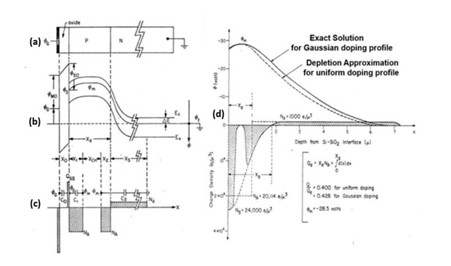
Figure 12
The electrostatic potential and the charge distribution
in Buried Channel CCD obtained by time domain (t) and
two dimensional ( x, y ) numerical computation solving
simultaneously the Poisson Equation in the ( x, y ) domain
and the continuity equation in the ( t, x ) domain.
Figure 13
NP junction type photodiode at the thermal equilibrium with
a heavily doped region in each side forming an Ohmic contact,
pinned by the external aluminum metal terminal voltage. The
charge carriers can pass thru the Schottky barrier by tunneling
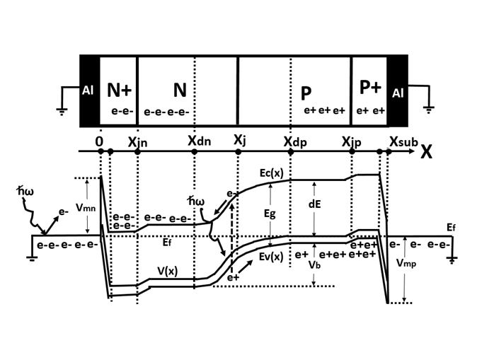
Figure 14
Schottky Barrier NP junction type photodiode with a transparent
metal electrode with the partially filled N type buried channel
charge collection and storage region.
Figure 15
Schottky Barrier NP junction type photodiode with a transparent
metal electrode with the completely empty N type buried channel
charge collection and storage region by complete charge transfer
operation mode to the adjacent charge transfer device (CTD).
The dashed line shows the potential of the charge collection
region at the full capacity and the Shotkky barrier is forward
biased and the excess overflowing signal charge can be drained
to the gate terminal. Hence this Shottky barrier PN junction
photodiode has a built-in vertical overflow drain (VOD) function.
Figure 16
Schottky Barrier NP junction type Photodiode with the
built-in vertical overflow drain (VOD) function, drawn
by Hagiwara at Sony, in Japanese Patent 1975-134985,
(Nov 10, 1975 ) which was used in Interline Transfer
Buried Channel CCD image sensor.
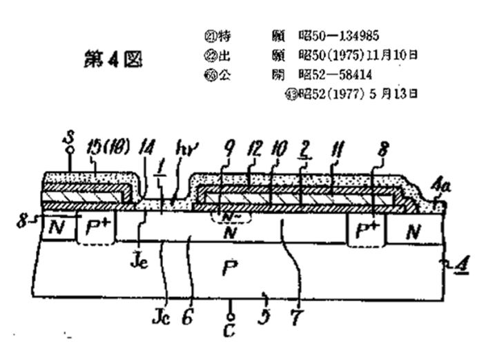
Figure 17
The Buried Vertical Overflow Drain (VOD) protection,
drawn in the USA patent USP3896485 ( July 22, 1975 )
by James M. Early at Fairchild, USA, applied in the
Surface Channel CCD Image Sensor.
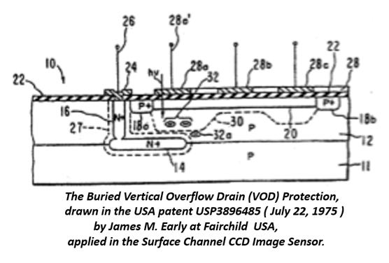
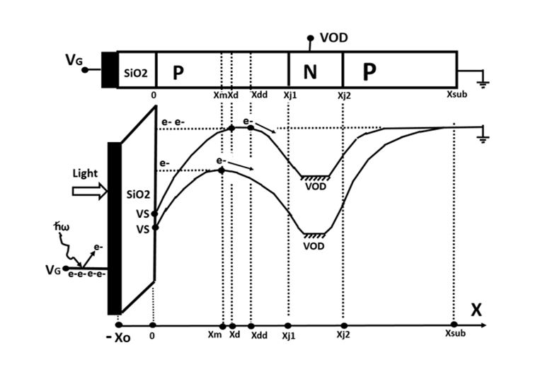
Figure 18
The electrostatic potential of the MOS capacitance type
photodiode with the Buried Vertical Overflow Drain (VOD)
protection , in the USA patent USP3896485, invented
( July 22, 1975 ) by James M. Early at Fairchild, USA,
applied in the Surface Channel CCD Image Sensor.
Return to AIPS HOMEPAGE TOP
return to the AIPS HOME PAGE TOP