**********************
The AIPS ( Artificial Intelligent Partner System ) Home Page 012
hagiwara-yoshiaki@aiplab.com
Return to http://www.aiplab.com/
**********************
For full English versions, please visit the following sites.
Story of Pinned Photo Diode (html)
Hagiwara at SONY is the true inventor of Pinned Photo Diode (html)
See also ElectronicsStackExchangeSite on "What is Pinned Photo Diode ? "
Pinned Photo Diode was invented by Hagiwara of Sony in 1975 (PDF)
**********************
**************************************
特別半導体技術講座 「イメージセンサー、賢い電子の目」 の復習用質問リストです。
Basic Review Question List on the Image Sensor, the Smart Electric Eye.
**************************************
***********************
PART ONE 半導体物性基礎
***********************
(001) 金属とは?
Q001 What is a metal ?
(002) 光電効果とは?
Q002 What is the photo electron effect ?
(003)金属のWork Function とは?
Q003 What is the Work Function in metal ?
(004) コンデンサーとは?
Q004 What is the capacitor ?
(005) 誘電率とは?
Q005 What is permittivity ?
(006) 抵抗とは?
Q006 What is resistor ?
(007) 抵抗率とは?
Q007 What is resistivity ?
(008) 半導体とは? Energy Gap とは?
Q008 What is Eneryg Gap ?
(009) Donor型不純物金属とは?
Q009 What is the Donor type impurity metal atom ?
(010) Acceptor型不純物金属とは?
Q010 What is the Accepor type impurity metal atom ?
***********************
PART TWO 半導体素子基礎
***********************
(011) N型半導体とは?
Q011 What is the N type semiconductor ?
(012) P型半導体とは?
Q012 What is the P type semiconductor ?
(013) Donor型とAcceptor型不純物金属のペアとは?
Q012 What is the Pair of the Donor type and Acceptor type impurity metal atoms ?
(014) PN接合とは? NP接合とは?
Q014 What is a PN junction ? What is a NP junction ?
(015) 空乏層とは?
Q015 What is a depletion layer ?
(016) Bipolar Transistor とは?
Q016 What is a Bipolar Transistor?
(017) Bipolar Transistor の ON 抵抗とは?
SONYの川名喜之さん発明の「中ぐり製法」とは?
Q017 What is the ON resistor of a Bipolar Transistor?
What is the silicon chip back side center thinning method
which was invented by Yoshiyuki Kawana at Sony ?
(018) Bipolar Transistor の入力抵抗とは?
Q018 What is the input resistor of a Bipolar Transistor?
(019) SONY の Transistor の開発史を知っていますか?
Q019 Do you know the history of the SONY Efforts for Transistor Developments ?
(020) Ge Transistor とは? Silicon Transistor とは?
米国 Texas Instrument 社のキルビー特許とは?
Q020 What is Ge Transistor ? What is Si Transistor ?
米国 Texas Instrument 社のキルビー特許とは?
*************************
PART THREE 半導体回路基礎
*************************
(021) Emitter Follower 回路とは?
Q021 What is Emitter Follower circuit ?
(022) Bipolar Transistor の線形増幅回路とは?
Q022 What is Bipolar Transistor Linear Amplifier circuit ?
(023) Planor Transistor とは?
Q023 What is Planor Transistor ?
(024) MESA Transistor とは?
SONYの加藤俊夫さん発明のAdvance Passivation MESA 製法とは?
Q024 What is MESA Transistor ?
What is the Advanced Passivation MESA fabrication method
which was invented by Toshio Kato at Sony ?
(025) MOS Transistor とは?
Q025 What is MOS Transistor ?
(026) Pass Transistor とは?
Q026 What is Pass Transistor ?
(027) MOS Transistor の入力容量とは?
Q027 What is the input capacitance of an MOS Transistor ?
(028) 自己整合型 Source/Drain MOS プロセスとは?
Q028 What is the self sligned Souce/Drain Formation type MOS fabrication process ?
(029) Source Follower 回路とは?
Q029 What is Source Follower circuit ?
(030) Inverter 回路とは?
Q030 What is Inverter circuit ?
*******************************
PART FOUR 半導体デジタル回路基礎
*******************************
(031) NAND 回路とは? AND 回路とは?
Q031 What is NAND circuit ? What is AND circuit ?
(032) NOR 回路とは? OR 回路とは?
Q032 What is NOR circuit ? What is OR circuit ?
(033) 比較回路とは?
高速並列処理128 bit dara stream 比較回路とは?
Q033 What is a comparator circuit ?
What is the fast pararell 128 bit digital data stream comparator circuit ?
(034) Shift Register 回路とは?
Q034 What is a Shift Register circuit ?
(035) Memory 回路とは?
Q035 What is a Memory circuit ?
(036) SRAM 回路とは?
どこの会社が世界で最初にSRAM chipの商品化に成功したのか?
Q036 What is a SRAM circuit ?
Which company made the SRAM chip business for the first time ?
(037) DRAM回路とは?
どこの会社が世界で最初にDRAM chipの商品化に成功したのか?
Q037 What is a DRAM circuit ?
Which company made the DRAM chip business for the first time ?
(038) DRAM回路の開発歴史を知っていますか?
Q038 Do you know the history of the DRAM Circuit Development Efforts ?
(039) MOS Image Sensor の開発歴史を知っていますか?
Q039 Do you know the history of the MOS Image Sensor Development Efforts ?
(040) MOS Image Sensor の問題点は何だったのでしょうか?
Q040 What were the problems of the MOS Image Sensor ?
*******************************
PART FIVE 半導体固体撮像素子基礎
*******************************
(041) どうして CCD Image Sensor が Super Star になったのでしょうか?
Q041 Why and how did the CCD Image Sensor become the Super Star ?
(042) SONY の CCD Image Sensor の開発史を知っていますか?
Q042 Do you know the history of the SONY CCD Image Sensor Develoment Efforts ?
(043) CCD Image Sensorを支えた重要な技術は何だったのでしょうか?
Q043 What were the supporting techology behind the curtain for CCD Image Sensors ?
(044) SONYのCCD Image Sensor搭載デジカメの開発史を知っていますか?
Q044 Do you know the history of the SONY CCD type Digital Camera Develoment Efforts ?
(045) どうして CCD Image Sensor が 急に ビデオカメラ市場から消えたのでしょうか?
Q045 Why did the CCD Image Sensor disappear from the video camera market suddenly ?
(046) どうして CMOS Image Sensor が Super Star になったのでしょうか?
Q046 Why and how did the CMOS Image Sensor become the Super Star ?
(047) CMOS Image Sensorを支えている重要な技術は何なのでしょうか?
Q047 What were the supporting techology behind the curtain for CMOS Image Sensors ?
(048) SONY original HAD sensor とは? Pinned Photo Diode とは?
Q048 What is SONY original HAD sensor ? What is the Pinned Photo Diode ?
(049) 今のSONYの半導体技術の強みはどこから生まれたのですか?
Q049 Where did the strength of SONY Semiconductor Technology come from ?
(050) 半導体は文明にエンジンであり、SONYの力の根源でもあります。今その未来はどこへ?
Q050 The semiconductor technology is the Engine of our Civilization,
and the Semiconductor Technology is also the Source of SONY Power.
Where is the future of the SONY Semiconductor Technology going now ?
以上です。
*************************************
この講義に関する参考文献のLISTです。
*************************************
*******************************************************************
See three invited talks related to SONY HAD sensor now called also as Pinned Photo Diode.
(1) International Conference CCD79 in Edinburgh, Scotland UK
(2) International Conference ESSCIRC2001 in Vilach, Austria.
(3) International Conference ESSCIRC2008 in Edinburgh, Scotland UK
*******************************************************************
Hagiwara was invited in these international conferences because of his contributions
to the image sensor community and related digital system LSI chip design works.
*******************************************************************
**********************************************************************
SONYの萩原良昭が1975年に出願したPinned Photo Diode の発明特許以前の
固体撮像素子の開発研究に関する重要な学会発表論文リスト
**********************************************************************
J.Bardeen and W.H.Brattain, "Transistor: A Semiconductor Triode",
Physical Review, VOl.74, p.230, July 1948.
W.Shockley, "The theory of p-n Junction in Semiconductor and p-n
Junction Transistor", Proc. IEEE Vol.51, pp.1190-1202, September 1949.
S.R.Hofstein and F.P.Heiman, "The Siliocn Insulated-Gate Field Effect
Transistor", Proc. IEEE Vol.51, pp.435-1202, September 1963
Gordon E. Moore, "Cramming more components onto integrated circits", Electronics,
Vol.38, No.8, April 19, 1965.
M.A.Schuster and G.Strull, " A Monolithic Mosaic of Photo Sensors for Solid
State Imaging Application", IEEE Trans. Electron Devices, Vol.ED-13, No.12, 1966
A. S. Grove, “Physics and Technology of Semiconductor Devices,”
John Wiley and Sons, Inc., New York pp.136-140, no.267, 1967.
P.K.Wiener, et al "A self-Scanned Solid State Image Sensor", in Proc. IEEE,
Vol 55, No.9, 1967.
G.P.Weckler, "Operation of PN Junction Photo Detectors in a Photon Flux
Integrating Mode", IEEE J. Solid State Circuits. Vol2, pp.65-73, September 1967.
P.J.W. Noble, "Self-Scanned Silicon Image Dector Arrys", IEEE Trans. Electron
Devices, Vil.ED-15, No.4, pp.202-209,1968.
S.G. Chamberlain, "Photosensitivity and Scanning of Silicon Image Detector
Arrays" IEEE J.Solid State Circuits, Vol.SC-4, No.6, pp.333-342, 1969.
F.L.J.Sangster and K.Teer, "Bucket Brigate Electronics - New Possibilities
for Delay Time-Axis Conversion and Scanning", IEEE J.Solid-State Circuits,
VOl.SC-4, No.3, pp.131-136, 1969.
W. S. Boyle and G. E. Smith, “Charge-Coupled Semiconductor Devices,”
Bell Syst. Tech. J., 49, pp.587-593, 1970.
W.M.Regitz and J.Karp, "A Three-transistor-cell, 1024 bit, 500 nsec
MOS RAM", ISSCC1970, Feb. 1970
F.L.J. Sanger, "Integrated MOS and Bipolar Analog Delay Lines using
Bucket Brigate Capacitor Storage", ISSCC1970, pp.74-75, 185, Feb. 1970.
G.F.Amelio, M.F.Tompsett and G.E.Smith, "Experimantal Verification of the
Charge Coupled Semiconductor Devices", B.S.T.J.Vol.49,pp.587-593,Apr. 1970
W.M.Regitz and J.Karp, "A Three-transistor-cell, 1024 bit, 500 nsec
MOS RAM", IEEE JSSC, VOl.SC-5, No.5, pp.181-186, October 1970.
W.F.Kosonocky and J.G.Carns, " Charge Coupled Digital Circuits", ISSCC1971,
pp.161-163, February 1971
G. F. Amelio, W. J. Bertram, Jr., and M. F. Tompsett,
“Charge-Coupled Imaging Devices: Design Considera- tions,”
IEEE Trans. Electron Devices, ED-18, no.11, pp.986-992, 1971.
M.F.Tompsett, et al "Charge Coupled Imaging Devces Experimental Results",
IEEE Trans. Electron Devices, Vol. ED-18, No.11, pp.992-996, 1971.
J.E.Carnes, "Drift-Aiding Fringing Fields in Charge Coupled Devices", IEEE J.
Solid State Circuits, Vol.SC-6, No.5, pp.322-326, 1971.
W.F.Kosonocky and J.G.Carns, " Charge Coupled Devices" ISSCC1972,
pp.132-133, February 1972.
C.H.Sequin, "Blooming Supression in Charge Coupled Area Imaging" Bell Sys.
Tech. J., 51, oo. 1923-1926, 1972.
J.D.Plummer and J.D.Meindl, " A Low-Light-Level Self-Scanned MOS Image
Sensor" ISSCC1972 Dig.Tech.Paper pp.30-31, February 1972.
J. E. Carnes and W. F. Kosonocky,
“First Interface-State Losses in Charge-Coupled Devices,”
Appl. Phys. Lett., vol.20, pp.261-263, 1972.
J. E. Carnes and W. F. Kosonocky,
“Noise Sources in Charge-Coupled Devices,”
RCA Review, vol.33, pp.327-343, 1972.
R. H. Walden, R. H. Krambeck, R. J. Strain, J. McKenna,
N. L. Schryer, and G. E. Smith, “The Buried Channel Charge
Coupled Devices,” Bell Syst. Tech. J., no.51, pp.1635-1640, 1972.
G. F. Amelio, “Physics and Applications of Charge Coupled Devices,”
IEEE INTERCON, New York, Digest, vol.6, paper 1/3, 1973.
D. M. Erb, W. Kotyczka, S. C. Su, C. Wang, and G. Clough,
“An Overlapping Electrode Buried Channel CCD,”
IEDM, Washington, D.C., Tech. Digest, pp.24-26, 1973.
W. F. Kosonocky and J. E. Carnes,
“Two Phase Charge Coupled Devices with Overlapping Polysilicon
and Aluminum Gates,” RCA Review, vol.34, pp.164-202, 1973.
D.M.Erb,W.Kotyczka, S.C. Su, C.Wamg and G.Clough, "An Overlapped
Electrode Buried Channel CCD", IEDM1973, Dec 3-5, 1973.
S. R. Shortes et al., “Development of a thinned backsideilluminated
charge-coupled device image,” in Proc. IEDM1973, Dec. 1973, p. 415.
N.G. Vogi, et al "A Half-Million Pel Bucket Brigate Optical Scanner",
ISSCC1974, pp. 30-31, February 1974.
P. A. Gray and H. Coltman, “Back surface imaging of thinned CCDs,”
in Proc. CCD, 1974, pp. 162–167.
J. Lohstroh, "The JFET as a Photosensitive Cell in Image Sensor Arrys",
ISSCC1974, pp. 34-35, February 1974.
M.H. White, "Characterization of Surface CHannel CCD Image Arrays at
Low Light Level", IEEE J. Solid State Circuits, Vol.SC-9, No.1, pp.1-12, 1974.
A. W. Lees and W. D. Ryan, “A Simple Model of a Buried-Channel
Charge-Coupled Device,” Solid-State Electron., vol.17, pp.1163-1169, 1974.
C. H. Sequin, F. J. Morris, T.A. Shankoff, M. F. Tompsett, and E. J. Zimany,
“Charge-Coupled Area Image Sensor Using Three Levels of Polysilicon,”
IEEE Trans. Electron Devices, ED-21, pp.712-720, 1974.
M. H. White, D. R. Lampe, F. C. Blaha, and I. A. Mack,
“Characterization of Surface Channel CCD Imaging Arrays
at Low Light Levels,” IEEE Trans. Solid-State Circuits,
SC-9, pp.1-13, Feb. 1974.
D. F. Barbe, “Imaging Devices Using the Charge-Coupled Concept,”
Proc. IEEE, vol.63, no.1, pp.38-67, 1975.
C. H. Sequin and M. F. Tompsett, “Charge Transfer Devices,”
Academic, New York, 1975.
James M. Early ( Fairchild Camera and Instrument Corporation, USA ) "Charge
Coupled Device with Overflow Protection", USP 3896485, July 22, 1975.
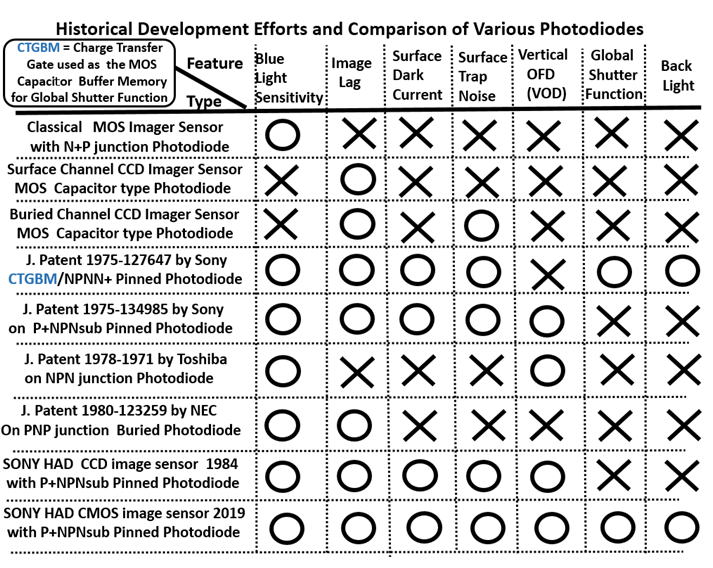
Hagiwara had to protect his 1975 Japanese patent ( 1975-127647 )
on the P+NPNsub Junction (Thyristor ) type Light Detecting Picture
Cell Structure agaist this Fairchild Early USP 3896485 patent.
The SONY-Fairchild Patent War lasted from 1991 till 2000.
Finally, Sony won the Patent war over Fairchild. But during the
long period of 10 years, Hagiwara felt as if he was in Jail and
could not perform any important job tasks in Sony at all.
**********************************************************************
SONYの萩原良昭が1975年に出願した
Pinned Photo Diode の発明特許に関する重要な学会関連技術発表リスト
**********************************************************************
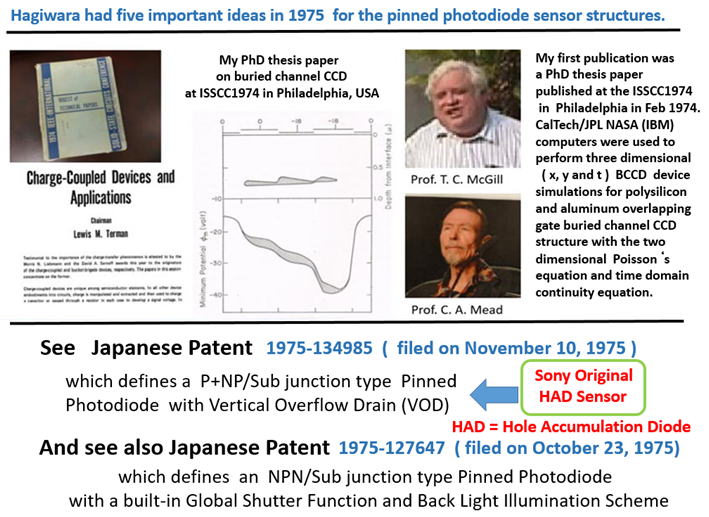
Hagiwara ISSCC1974 Paper on "Buried Channel CCD Charge Transfer"
February 1974 in Philadelphia, USA. This was Hagiwara PhD thesis paper
at California Institute of Technology (CalTech) Pasadena, California USA>
Hagiwara, 1975 Japanese Patent ( JA 1975-127647 ) at SONY
on the Pinned Photo Diode with Back Light Illumination
Hagiwara, 1975 Japanese Patent ( JA 1975-134985 ) at SONY
on the Pinned Phodo Diode with Vertical Overflow Drain Function
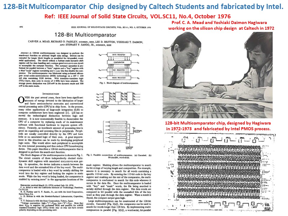
C.A.Mead, R.D.Pashley,Lee D. Britton, Yoshiaki T.Daimon Hagiwara and
S.F. Sando, "128-Bit Multicomparator", J. Solid State Circuits, Vol.SC-11,
No.5, October 1976. This is important for intelligent image sensor systems.
Hagiwara, 1978 Solid State Semiconductor Device Conference Paper on
"Narrow Channel Frame Transfer CCD Image Sensor" at Tokyo, Japan .
This is the first paper in the world reporting the P+NP type ( dynamic
PNP junction ( photo transistor ) type light detecting picture element
structure, which was later called as the Pinned Photo Diode.
Y. Daimon-Hagiwara, M. Abe, and C. Okada, “A 380Hx488V CCD imager
with narrow channel transfer gates,” Japanese J. Appl. Phys., vol. 18,
supplement 18–1, pp. 335–340, 1979.
Hagiwara, CCD'79 invited paper on "SONY Image Sensor Efforts"
at Edinburgh, Scotland UK on SONY CCD image sensors.
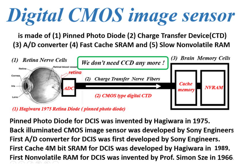
Fumio Miyaji, Yasushi Matsuyama, Yoshikazu Kanaishi, Katsunori Senoh,
Takashi Emori and Yoshiaki Hagiwara, "A 25 nanosec 4 Mega bit CMOS
RAM with DYnamic Bot-Line Loads", ISSCC1989 and J.Solid State Circuits,
Vol24, No.5, October 1989. This wad for Cache SRAM memory for SONY
Compact Digital CCD Image Sensors.
Y. Hagiwara, “High-density and high-quality frame transfer CCD imager
with very low smear, low dark current and very high blue sensitivity,”
IEEE Trans. Electron Devices, vol. 43, no. 12, pp. 2122–2130, Dec. 1996.
Hagiwara, ESSCIRC2001 invited paper on "SONY Consumer Electronics"
at Vilach, Austria
Hagiwara, ESSCIRC2008 invited paper on "SOI Cell Processor and Beyond"
at Edinburgh, Scotland UK
Hagiwara, the 60th Aniversary ISSCC2013 Plenary Panel Talk,
at San Franicisco, USA
**********************************************************************
SONYの萩原良昭が1975年に出願した
Pinned Photo Diode の発明特許に関する頃の、時代背景について。
**********************************************************************
この国際学会で萩原は1975年発明の Pinned Photo Diodeの構造を
説明し、CCDの超感度低案電流は萩原考案の光感知素子の特徴で
あり、CCD自体は金属電極があり光感知素子には不向きであると論じ
ています。しかし一般メディアはCCDが高感度だと誤解したままでした。
1978年の初夏でした。萩原1975年発明のPinned Photo Diode 搭載の
FT型CCD Image Sensor の一体化ビデオカメラをSONYは新聞発表。
盛田会長が自らNewYorkで、岩間社長が自らTokyoで、同時に、
Press Conference を開催し、多くの新聞・テレビ・雑誌記者の前で、
大きく、新しい民生用小型ビデオカメラの時代を宣言しました。
しかし、ここでも、盛田会長と岩間社長は一般メディアに対しては
全体としてCCD Video Camera が高感度であることには変わりが
ないことから、一般メディアはCCDが高感度だと誤解したままでした。
ソニーは、萩原設計の 2-chip型の Interline 方式のCCD image
sensor の商品化に成功し、全日空(ANA)のジャンボジェット機の
コックピットに搭載し、飛行機の離着陸時の様子を機内のビデオ
スクリーンで迫力ある、real time の映像を見ることができました。
この 2-chip型の Interline 方式のCCD image sensor は 透明
電極を使用し、横型OFD構造でした。受光部は透明電極を使用
したCCD型の光感知素子構造を採用しており、CCDの完全空乏化
電荷転送により残像のない、Interline 方式のCCD image sensor
をSONYは既に1980年に実用化してビデオカメラに搭載しています。
その成果は国内学会でのみの発表が許可されました。
狩野、安藤、松本、萩原、橋本、 ”インターライン転送方式CCD撮像素子”
テレビジョン学会、電子装置研究会 ED 481, pp.47-52, Jan 24, 1980.
SONYの開発部隊は総力をあげて、この残像なしの、インターライン転送
方式CCD撮像素子の One Chip 化に取り組んでいました。
同時に、萩原1975年発明の Pinned Photo Diode の光感知素子
構造も、萩原1975年特許の中で説明している様に、CCDでなくても、
このPinned Photo Diode の光感知素子構造も、完全空乏化電荷
転送により残像がありません。かつ、光感度はCCD型よりもはるかに
超感度です。CCD型では、シリコン界面に強い電界がかかり、表面
再結合準位の存在の為に、CCD型では表面結合の暗電流が多い
でしたが、この萩原1975年発明の Pinned Photo Diode の光感知
素子構造では、表面は外部から電圧固定(ピン止め)されていて
電界がかからず、表面再結合準位が不活性(quench)され、表面
再結合による暗電流がありません。また表面捕獲準位の影響も
受けず、 trap 雑音、 1/f 雑音もない、超感度で低雑音を実現
しています。
ソニーは、当初から本命とされ、萩原が設計を担当し、その後、後輩の
竹下さんがその技術技術を継承した、 One chip の Interline 方式の
CCD Image Sensorの開発生産技術と信頼性技術に全力を注ぎました。
そして、世界発のPassportサイズの小型ビデオカメラの試作生産販売を
成し遂げました。ビデオカメラの市場を制覇、独占しました。
萩原1975年発明の、この高性能光感知素子構造が CCD Image Sensor
欠点を助け、CCDの延命に長く寄与しました。そして、その勢いは現在も継続し、
SONY Brand 商標の SONY original HAD sensor 搭載の CMOS Image
Sensor の技術力と生産力の基礎となっています。
さらに裏面照射型のPinned Photo Diode は、1975年萩原がこの特許の中で
世界で初めて構想していたもので、現在の「賢い電子の目」の実現の源点です。
Hagiwara, CCD'79 invited paper on "SONY Image Sensor Efforts"
at Edinburgh, Scotland UK on SONY CCD image sensors.
この国際学会で萩原は1975年発明の Pinned Photo Diodeの構造を
説明し、CCDの超感度低案電流は萩原考案の光感知素子の特徴で
あり、CCD自体は金属電極があり光感知素子には不向きであると論じ
ています。しかし一般メディアはCCDが高感度だと誤解したままでした。
この開発研究チームは国内の学会でその詳細を発表しています。
平田、大津、阿部、萩原、 "2/3 inch 狭チャンネルCCD撮像素子", テレビジョン
学会、テレビジョン方式・回路研究会 TEBS69-3, 電子装置研究会 ED 555,
pp.13-18, Feb. 27, 1981.
島田、梶野、西村、小室、中田、南、"狭チャンネルFT型CCDによる単板カラー
カメラ",テレビジョン学会、テレビジョン方式・回路研究会 TEBS70-4, Sept.8, 1981.
Hagiwara, ESSCIRC2001 invited paper on "SONY Consumer Electronics"
at Vilach, Austria
Hagiwara, ESSCIRC2008 invited paper on "SOI Cell Processor and Beyond"
at Edinburgh, Scotland UK
Hagiwara, the 60th Aniversary ISSCC2013 Plenary Panel Talk,
at San Franicisco, USA
**********************************************************************
CCDの開発商品化を世界の多くの企業が断念し諦める中、SONYは世界で一社のみで
"Never Give Up " の精神で独走していました。その成果はSONYの次の国内論文の嵐
を引き起こしました。
ます、1978年のSONYの一体化ビデオカメラの発表が最初の花火でした。
その技術内容は東京で開催の国際固体素子コンファレンス1979年でまず
世界に紹介されました。
Y. Daimon-Hagiwara, M. Abe, and C. Okada, “A 380Hx488V CCD imager
with narrow channel transfer gates,” Japanese J. Appl. Phys., vol. 18,
supplement 18–1, pp. 335–340, 1979.
そして、萩原は、その発明開発技術者として、 Scotland UK の Edinburgh 大学で
開催の、CCDの国際会議 CCD79に、招待講演の招待を受けました。
Hagiwara, CCD'79 invited paper on "SONY Image Sensor Efforts"
at Edinburgh, Scotland UK on SONY CCD image sensors.
その後、SONYはさらに次々とCCDの開発成果を発表しました。
狩野、安藤、萩原、橋本、”インターライン転送方式CCD撮像素子”、
テレビジョン学会、電子装置研究会 ED481、pp. 47-52、Jan 24, 1980
名雲、山中、越智、”CCD カラーカメラの線順次撮像方式と信号処理方式”、
テレビジョン学会技術報告書 TEBS 60-1, pp. 19-25, Jan 25, 1980
村田、名雲、中田、安井、西村、小室、粂沢、”線順次 2CCDカラーカメラ”、
テレビジョン学会、テレビジョン方式・回路研究会 TEBS 60-2, pp. 27-32, Jan 25, 1980
この3つの国内論文の技術内容は国際学会にも以下の2つの論文の形でも発表されました。
F.Nagumo, T.Asada and S.Ochi, " CCD Digital Color Camera ", IEEE Transaction
on Consumer Electronics, VOL.CE-26, No.8, pp. 339-352, Aug. 1980.
T.Asada and F.Nagumo, " A New Digital CCD Color Camera using Direct Encoding
Method", International Conference on Digital Signal Processing " Florence, Italy,
September 2 - 5 , 1980.
また、同時に構内では、やっと社内で One chip CCD カメラの
実際の技術開発者による、技術詳細の発表の許可がおりました。
平田、大津、阿部、萩原、 "2/3 inch 狭チャンネルCCD撮像素子", テレビジョン
学会、テレビジョン方式・回路研究会 TEBS69-3, 電子装置研究会 ED 555,
pp.13-18, Feb. 27, 1981.
島田、梶野、西村、小室、中田、南、"狭チャンネルFT型CCDによる単板カラー
カメラ",テレビジョン学会、テレビジョン方式・回路研究会 TEBS70-4, Sept.8, 1981.
しかし、その成果は会社全体の業績として、会社での開発TOP管理責任者の
実績として記録されることになりました。萩原をはじめ多くの萩原を支援して
くれた技術者陣が総力で成し遂げた仕事の成果実績を、会社のTOの森尾さん
と越智さんにピンはねされた瞬間でした。
”SONYの森尾、越智、土井の3氏にエドアルドライン賞”、毎日新聞、9月8日、1981.
実際には、以下の2つの仕事にも、萩原の開発した Image Sensorが搭載され、
採用されていますが、萩原とその協力技術者の業績の引用(citation) は皆無です。
”フィルム不要のカメラ 磁気ディスクで50枚撮れる、プリントOKカメラ屋さん脅威、
ソニーが開発”、読売新聞、8月25日、1981.
J. Marcom Jr. "Sony unveils a Camera that Doesn't Use Film", Asian
Wall Street Journal, August 26, 1981.
木原、斎藤、浦原、中田、岡本、中鉢、”マビカシステム”、テレビジョン学会技術
報告 TEBS 80-5 , VR 50 - 5, pp. 25-31, March 25, 1981 .
その後、SONYは、萩原のオリジナル設計のCCD Image Sesnor を採用した、
マビカの商標名でデジタルマビカを商品展開し、市場を驚かせた。
実は、そのマビカの商標名の名づけの親は萩原自身だった。
当時、萩原がSONYの中研時代に、商品名称の社員公募があった時、萩原が、
Magnetic Video Camera を略して、MAVICAと命名し、応募し、偶然にも、それが
採用された事実がある。萩原はたいへん喜んだ。
たいへん偶然の、名誉あることだと萩原は感じた。その事は公募作業担当者以外、
まったく誰にも知られないことであった。しかし、萩原はSONYのデジタルマビカの
大の愛好者で、海外出張の時には必ず持って出かけた。母校のCalTechを訪問し、
恩師の Prof. T.C. McGIll や、 Prof. C.A. Mead も、大の愛好家であることを
知り、萩原はたいへん満足で幸せな気分だった。♡
**********************************************************************
**********************************************************************
SONYの萩原良昭が1975年に出願したPinned Photo Diode の発明特許以後の
固体撮像素子の開発研究に関する重要な学会発表論文リスト
**********************************************************************
Gilbert F. Amelio ( Fairchild Camera and Instrument Corporation, USA )
"Self Aligned CCD Element including Two Levels of Electrondes and
Method of Manufacture therefor" USP 3931674, Jan 13, 1976.
This Amelio patent (USP3931674) which was judged invalid by the prior
art of USP3745647 by Boleky and by IEDM1973 paper by D.M.Erb,
W.Kotyczka, S.C.Su, C.Wamg and G.Clough, "An Overlapped Electrode
Buried Channel CCD", IEDM1973, Dec 3-5, 1973.
T. Yamada, H. Okano, and N. Suzuki, “The Evaluation of Buried Channel Layer
in BCCD’s,” IEEE Trans. Electron Devices, ED-25, no.5, pp.544-546, 1978.
J. Hynecek, “Virtual phase CCD technology,” in Proc. IEDM1979, pp. 611–614,
Dec. 1979,
J.Nishizawa, et al, "Static Induction Transistor Image Sensors", IEEE Trans.
Electron Devices, Vol.ED-26, No.12, pp.1970-1977, 1979.
A. Furukawa, Y. Matsunaga, N. Suzuki, N. Harada, Y. Endo, Y. Hayashimoto, S. Sato,
Y. Egawa, and O. Yoshida, “An Interline Transfer CCD for A Single Sensor 2/3” Color
Camera,” IEDM, Washington, D. C., Tech. Digest, pp.346-349, 1980.
K.Hoshi, T.Suzuki, Y.Okubo and N.Isawa, "CZ Siliocn Crystal grown in Transverse
Magnetic Fields", 157th ECS Mtg Ext. Abstract, pp.811-813, May 1980.
T.Asada and F.Nagumo, "A New CCD Digital Color Camera using Direct Encoding
Method", Int. Conf. on Digital Signal Processing, September 2-5, 1981, Florence Italy.
Y. Ishihara, E. Oda, H. Tanigawa, N. Teranishi, E. Takeuchi, I. Akiyama, K. Arai,
M. Nishimura, and T. Kamata, “Interline CCD Image Sensor with an Anti Blooming
Structure,” ISSCC Digest of Technical Papers, pp.168-169, Feb. 1982.
N. Teranishi, A. Kohno, Y. Ishihara, E. Oda, and K. Arai, “No Image Lag Photodiode
Structure in the Interline CCD Image Sensor,” IEDM Tech. Dig., pp.324-327, 1982.
Y.Ishihara and K.Tanigaki,"A High Photosensitivity IL-CCD Image Sensor with
Monolithic Resin Lens Array", IEDM1983 Tech. Dig, pp.497-500, December 1983.
B.C. Burkey et al, "The Pinned Photo Diode for an Interline Transfer Image Sensor",
IEDM1984, DIg.Tech.Papers, pp.28-31, December 1984.
K. Horii, T. Kuroda, and S. Matsumoto, “A New Configuration of CCD Imager with a
Very Low Smear Level -FIT-CCD Imager,” IEEE Trans. Electron Devices, ED-31, no.7,
pp.904-909, 1984.
Y. Matsunaga and N. Suzuki, “An Interline Transfer CCD Imager,” ISSCC Digest of
Technical Papers, pp.32-33, Feb. 1984.
M.Ogawa et al, "Signal-PRocesiing ICs employed in a Single-Chip CCD Color Camera",
IEEE TRansaction on Consumer Electronics, Vol.CE-30, No.3, pp.374-381, Aug.1984
T.Kumezawa et al, "High Resolution CCD Image Sensors with Reduced Smear", IEEE
transaction on Electron Devices, VOl. ED-32, No.8, pp.1451-1456,1618, Aug. 1985.
Y.Ogawa et al, "Development of CCD Imaging Block for Single Chip Color Camera",
IEEE Transaction on Consumer Electronics, Vol.CE-31, No.3, pp.405-413, Aug. 1985
T.Nakamura,"A New MOS Image Sensor Operating in a Non-destructive Readout
Mode", IEDM1986, Tech.Dig. pp.353-356, December 1986.
M.Yamamura et al, "A 1/2 inch CCD Imager with 510 x 492 pixels", SPIE Vol.765
Image Sensors and Displays pp.41-46, Jan 13-14, 1987.
T. Yamada, K. Ikeda, and N. Suzuki, “A Line-Address CCD Image Sensor,”
ISSCC Digest of Technical Papers, pp.106-107, Feb. 1987.
T. Yamada, T. Yanai, and T. Kaneko, “2/3 Inch 400,000 Pixel CCD Area Image Sensor,”
Toshiba Review, no.162, pp.16-20, Winter 1987.
N. Teranishi and Y. Ishihara, “Smear Reduction in the Interline CCD Image Sensor,”
IEEE Trans. Electron Devices, ED-34, no.5, pp.1052-1056, 1987.
A.J.P.Theuwissen et al, "A 400K Pixel 1/2 inch Accorion CCD Imager", ISSCC1988,
Dig.Tech.Papers, pp.48-49, February 1988.
M. Hamasaki, T. Suzuki, Y. Kagawa, K. Ishikawa, M. Miyata, and H. Kambe,
“An IT-CCD Imager with Electronically Variable Shutter Speed,” ITEJ Technical
Report, vol.12, no.12, pp.31-36, 1988.
H.Yamashita et al, "A New High Sensitivity Photo-transitor for Area
Image Sensors", IEDM1988 Tech Dig pp.353-356, December 1988.
J.Hynecek, "A New Device Architecture Suitable for High-Resolution
and High Performance Image Sesnors", IEEE Trans, Electron Devices,
Vol.35, No.5, pp.646-652, 1988.
N.Tanaka, et al,"A Novel Bipolar Imaging Device with Self-NOise Reduction
Capability", IEEE Trans. Electron Devices, Vol.36, No.1, pp.31-38, 1989
K.Yonemoto et al, "A 2 million Pixel FIT-CCD Image Sensor for HDTV
Camera System" IEEE ISSCC1990, pp.214-216, February 1990.
F.Andoh et al,"A 250 000 Pixel Image Sensor with FET Amplification
at Each Pixel for High Speed Television Cameras", ISSCC1990, Dig.Tech.Papers
pp.212-213, February 1990.
Eric G. Stevens et al, "A One Mega Pixel Progressive Scan Image Sensor with
Antiblooming Control and Lag-Free Operation", IEEE Trans. Electron Devices,
Vol38, No.5, pp.981-988, 1991.
K.Ishikawa and T.Iizuka, "One inch 2M pixel CCD with Hyper HAD sensor and
Camera System for HDTV", SPIE proc. Vol. 1656, pp.30-40, February 1992.
T. Ishigami, A. Kobayashi, Y. Naito, A. Izumi, T. Hanagata, and K. Nakashima,
“A 1/2-in 380k-pixel Progressive Scan CCD Image Sensor,” ITE Technical Report
Vol.17, no.16, pp.39-44, Mar. 1993.
P.B.Denyer et al, "CMOS Image Sensors for Multimedia Applications", IEEE
Constum Integrated Circuits Conference 1993, Proc. of CICC1993,
pp.11.5.1-11.5.4, 1993.
H.Kawashima et al, "A 1/4 inch Format 250K Pixel Amplified MOS Image Sensor
Using CMOS Process", IEDM1993, Tech. Dig. pp.575-578, December 1993.
S.K.Mendis et al, "128 x 128 CMOS Active Pixel Image Sensor for Highly Integrated
Imaging Systems", IEDM1993, Tech. Dig. pp.583-586, December 1993.
E.R.Fossum,"Active Pixel Sensors: Are CCD's dinosaurs ?" , in Proc. SPIE,
Vol.1900, pp.2-14, 1993.
Hitachi MOS Image Sensor Engineers and Intel MOS Process
Engineers all knew that eventually the scaled down MOS Process
Technology will conquer all other kinds of Process Technologies
including CCD image sensor technology, because of the power
consideration and scaled down dimensional advantage of CMOS
process technology.
The three transistor CMOS active picture cell was already
invented as, since the three-transistor circuit is identical to,
the three-transitorcircuit of the DRAM cell, with the active
source follower type current amplification.
Fossum was just a commentator in his SPIE 1993 paper above,
emphasizing the fact and speculations that the original image
sensor experts and engineers all knew in 1970s.
Fossum did not the develop the compact digital CMOS image
sensors. Sony delligent engineering team did. Fossum was
just a commentator on the well known speculations.
R.H.Nixon et al, "128 x 128 CMOS Photodiode Type Active Pixel Sensor
with On-ChipTiming Ccntrol and Signal CHain Electronics", in Proc. SPIE,
Vol.2415, pp.117-123, 1995.
S. Kawai et al, "Photo Response Analysis in CCD Image Sensors with a VOD
Structure", IEEE TRans. Electron Devices, VOl.42, No.4, pp.652-655, 1995.
Paul P. K. Lee et al, "An Active Pixel Sensor Fabricated Using CMOS/CCD
Process Technology", in Proc. IEEE Workshop on CCDs and Advanced
Image Sesnors", 1995.
S.Kawahito et al,"A Compressed Digital Output CMOS Image Sensor with
Analog 2-D DCT Processors and ADC/Quantizer",ISSCC1997, Dig.Tech.Papers,
pp.184-185, February 1997.
T. H. Lee, R. M. Guidash, and P. P. Lee, “Partially pinned photodiode
for solid-state image sensors,” U.S. Patent 5,903,021, Jan. 1997.
R. M. Guidash, “Active pixel image sensor with shared amplifier
readout,” U.S. Patent no. 6,107,655, Aug. 1997.
Walter F. Kosonocky et al, "360 x 360 Element Three-Phase Very High
Frame Rate Burst Image Sesnor, Design, Operation and Perfomance",
IEEE Trans. Electron Devices, Vol.44, No.10, pp.1617-1624, 1997.
R.M.Guidash et al, "A 0.6 um CMOS Pinned Photo Diode Color Imager
Technology", IEDM1997, Tech. Dig. pp.927-929, December 1997.
M.Loinaz, et al, "A 200mW 3.3V CMOS Color Camera IC Producing
352 x 288 24b Video at 30 Frames/sec", ISSCC1998, Dig.Tech.Papers,
pp.168-169, February 1998.
Guang Yang, Orly Yadid-Pecht, Chris Wrigley, and Bedabrata Pain ,
"A Snap-Shot CMOS Active Pixel Imager for Low-Noise, High-speed
Imaging", IEDM1998, December 1998.
F.Andoh et al, "A Digital Pixel Image Sensor with 1 bit ADC and
8 bit Pulse Counter in Each Pixel", International Image Sensor
Workshop, P1, 1999.
K. Yonemoto et al, "A CMOS Image Sensor with a Simple FPN
Reduction Technology and a Hole Accumulation Diode", ISSCC2000,
Dig.Tech.Papers, pp.102-103, February 2000.
T. Yamada, Katsumi Ikeda, Y. G. Kim, H. Wakoh, T. Toma, T. Sakamoto,
K. Ogawa, E. Okamoto, K. Masukane, K. Oda, and M. Inuiya, “A progressive
Scan CCD Image Sensor for DSC Applications,” IEEE J. of Solid-State
Circuits, vol.35, no.12, pp.2044-2054, 2000.
M.Furuyama et al,"High Sensitivity and No Crosstalk Pixel Technology
for Embedded CMOS Image Sesnor", IEEE Trans. Electron Devices,
Vol.48, No.10, 2001.
T.Miida,"A 1.5 M Pixel Imager with Localized Hole-Modulation Method",
ISSCC2002, Dig.Tech.Papers, pp.42-43, February 2002.
T. GOji Etoh,"A CCD Image Sensor of 1Mframe/sec for Continuous
Image Capturing 103 Frames", ISSCC2002, Dig.Tech.Papers, pp.46-47,
February 2002.
T.Sugiyama et al, "A 1/4 inch QVGA Color Imaging and 3-D Sensing
CMOS Sensor with Analog Frame Memory", ISSCC2002,Dig.Tech.Papers,
pp.434-435, February 2002.
A. Theuwissen, "50 years of Solid State Image Sensors",
ISSCC2003, Dig.Tech. Papers, S26, February 2003.
I. Inoue et al., “Low-leakage-current and Low-operating-voltage
Buried Photodiode for a CMOS imager,” IEEE Trans. Electron Devices,
vol. 50, no. 1, pp. 43–47, Jan. 2003.
K.Mabuchi,N.Nakamura, E.Funatsu,T.Abe,T.Umeda,T.Hoshino,R.Suzuki,
H.Sumi, "CMOS Image Sensor Using a Floating Diffusion Driving Buried
Photo Diode", ISSCC2004, pp.112-113, February 2004.
H.Takahashi et al, "A 3.9 um Pixel Pitch VGA Format, 10 bit Digital
Image Sensor with 1.5 Transistor /Pxcel", ISSCC2004, pp.108-109, Feb. 2004.
M.Mori et al, "A 1/4 inch 2M Pixel CMOS Image Sensor with 1.75
Transistor/Pixel", ISSCC2004, pp.110-111, February 2004.
Nana Akahane, Rie Ryuzaki, Satoru Adachi, Koichi Mizobuchi,
Shigetoshi Sugawa, "A 200dB Dynamic Range Iris-less CMOS Image
Sensor with Lateral OverflowIntegration Capacitor using Hybrid Voltage
and Current Readout Operation", ISSCC2006, pp.300-301, Feb.7, 2006.
Shin Iwabuchi et al,"A Back illunated High Sensitivity Small Pixel
Color CMOS Image Sensor with Flexible Layout of Metal Wiring",
ISSCC2006, pp.302-303, Feb.7, 2006
Y. Nitta et al, "High Speed Digital Double Sampling with Analog CDS
on Column parallel ADC Architecture for Low Noise Active Pixel Sensor",
ISSCC2006, pp.500-501, Feb. 8, 2006
S.Yoshihara et al, "A 1/1.8 inchi 6.4 Mega Pixel 60 frames/sec CMOS
Image Sensor with Seamless Mode Change", ISSCC2006, Dig.Tech.Papers
pp.1984-1993, February 2006.
K.Cho et al, " A 1/2.5 inch 8.1 Mega Pixel CMOS Image Sesnor for
Digital Camera",ISSCC2007, Dig.Tech.papers pp.508-509, February 2007.
S-H Cho et al, "Optoelectronic Investigation for High Performance 1.4 um
pixel CMOS Image Sensors", International Image Sensor Workshop (IISW2007),
June 6-10, 2007.
Xinyang Wang, Padmakumar R.Rao, and Albert J.P. Theuwissen,
"Characterization of the Buried CHannel NMOS Source Followers
in CMOS Image Sesnors", International Image Sensor Workshop
(IISW2007), June 6-10, 2007.
Shoji Kawahito and Nobuhiro Kawai, "Column Parallel Signal
Processing Techniues for Reduing Thermal and RTS Noises in
CMOS Image Sensors", International Image Sensor Workshop
(IISW2007), June 6-10, 2007.
G.Agranov et al, "Super Small Sub 2 um Pixels for Novel CMOS
Image Sensors", International Image Sensor Workshop (IISW2007),
June 6-10, 2007.
J.Prima et al, "A 3 Mega Pixel Back illuminated Image Sensor
in 1T5 Architecture with 1.45 um Pixel Pitch", International
Image Sensor Workshop (IISW2007), June 6-10, 2007.
B.Cremers et al, "A High Speed Pipelined Snapshoto CMOS Image
Sensor with 6.4 Gpixel/sec Data Rate", International Image Sensor
Workshop 5.9, p.9, 2009.
K.Itonaga et al, "Extremely Low Noise CMOS Image Sensor
with High Saturation Capacity", IEDM2011, Dig.Tech.Papers
pp.171-174, December 2011.
M.Sakakibara et al,"An 83 dB Dynamic Range Single Exposure Global
Shutter CMOSImage Sensor with In-Pixek Dual Storage", ISSCC2012,
Dig.Tech.Papers, 22.1, pp.380-381, February 2012.
T.Tochigi et al, "A Global Shutter CMOS Image Sensor with Readout
Speed of One Tpixel/secBurst and 780 Mpixel/sec Continuous",
ISSCC2012, Dig.Tech.Papers, 22.1, pp.382-384, February 2012.
E.R.Fossum and D.B.Hondongwa, " A Review of the Pinned Photo Diode
for CCD and CMOS Image Sensors", IEEE J. of Electron Devices Society,
VOL-2, No.3, May 2014. This is a fake paper which did not quote the
Hagiwara 1975 patent on the Back Light Illuminated Pinned Photo Diode
Light Detecting Element Structure ( 1975-127647 ) with the complete
charge transfer operation mode with the image lag free feature. This
Fossum fake 2014 paper made also many false statements on the Hagiwara
1975 patent on the P+NPNsub junction (thysitor) type Pinned Photo Diode
Light Detecting Element Structure ( 1975-134985 ) that has the complete
charge transfer action with no image lag feature, and also with the built-in
vertical overflow drain (VOD) function.
Fossum is not the inventor of the active image sensor picture element.
Peter Noble is the inventor of the active image sensor picture element.
http://www.pjwn.co.uk/
*******************************************************************
Questions by Prof. Albert Theuwissen are ,
- who invented and developed the stitching technology
for large area image sensors ?
- who owns the world record in low-noise
in the voltage domain for CMOS Image Sensor (CIS) ?
Hagiwara believes that
Hagiwara invented and Sony diligent engineers developed the stitching technology
for large area image sensors. SONY called SONY original HAD sensor.
But the technical world ignored the SONY businesss Brand Name HAD, and
called it by another name, the Pinned Photo Diode.
Sony diligent engineers developed and now Sony owns the world record in low-noise
in the voltage domain for CMOS Image Sensor (CIS).
Teranishi did not invent the Pinned Photo Diode.
Hagiwara is the inventor of the Pinned Photo Diode.
Fossum is not the inventor of the active image sensor picture element.
Peter Noble is the inventor of the active image sensor picture element.
http://www.pjwn.co.uk/
******************************
***********************************************************************
*************************************
さて、冒頭での3つの基本質問の回答をここでします。
***********************************************
質問(1)
どうしてCCD image sensor が、今となっては過去になりますが、
ビデオカメラ業界ではスーパースターのように脚光を浴びる存在
だったのでしょうか?
***********************************************
Question (1)
Why was the CCD image sensor
the super star in the past ?
***********************************************
Answer :
埋め込みチャネル型のCCD の電荷転送効率は99.999% と
非常に高く、かつ、配線容量に起因するCkT 雑音は非常に低い。
The buried channel type CCD has a very high charge
transfer efficiency of 99.999% with very low CkT noise.
もう過去になりますが、昔のNTSC方式のTVシステムでは、
横の画素が720Hで、縦の画素が512Vでした。
それで、一番出力回路から遠い位置の絵素(光感知部)は、
720+512=1232回の電荷転送が最大必要となります。
In the past TV system of the 720 H x 512 V picture
resolution, we only needed the total of 1232 charge
transfers at most to transfer the signal charge from
the light detecting storage area ( the pinned photo
diode ) to the final chip output buffer circuits.
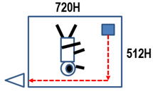
従って、最大でも、電荷転送効率が 99.999%ということは、
1回の電荷転送で 0.001 %の電荷が転送残りとなるという
ことですから、最終的に 1232回の電荷伝送では、1.232 %
の残像および混色問題が生じます。しかし、それを過去の
ビデオカメラシステムでは許容範囲としました。
Therefore, the incomplete charge transfer of
0.001 % x 1232 charge transfer gives 1.232 % of
the total incomplete charge transfer which means
only the 1.232% of image lag and color picture
contamination, which was tolerable in the past
video camera system.
かつ、配線容量による CKT 雑音が CCD image sensor の方が
当時の MOS image sensor のCKT 雑音よりはるかに小さく、
CCD image sensor の方が、当時は、 MOS image sensor より
はるかに魅力的な存在でした。
Besides, CCD image sensor has a very low CkT noise,
which is much lower than that of MOS image sensor.
***********************************************
質問(2)
どうして近年のハイビジョンのデジタルテレビ時代では、
CCD image sensor がどうして不要の存在になって
しまったのでしょうか?
***********************************************
Question (2)
Why is the CCD image sensor now obsolete
in the modern digital high vision TV era ?
***********************************************
Answer
埋め込みチャネル型CCDは CKT 雑音が たいへん小さいですが、
問題は、その電荷転送効率の値 99.999 %でした。この値では、
もはや充分な完全な電荷転送効率ではない時代になりました。
The buried channel type CCD has very low CkT noise,
but has only a limited charge transfer efficiency of
99.999%, which is now not good enough.
現在の高解像ハイビジョンTVシステムでは、たとえば,4Kテレビ
では、横3840H、縦2160V の解像度となり、出力回路に一番遠い
絵素(光感知素子=the pinned photo diode) から信号電荷を
CCDで転送するには、合計で、 3840 + 2160 = 6000 回の電荷
転送を実行する必要があります。
In the modern high resolution TV system, such as in the
4K TV system of the 3840H×2160V picture resolution,
we need the total of 6000 charge transfers at most to
transfer the signal charge from the light detecting storage
area ( the pinned photo diode ) to the final chip output
buffer circuits.
その為、転送残りは 0.001 % x 6000 = 6%にもなります。この
6%の電荷転送残りは残像にもなり、混色問題がさらに深刻となり、
より高解像で高品質画像を求めるハイビジョンTVシステムではもう
CCDは、利用価値がありません。もはや、CCDは不要な存在です。
Therefore, the incomplete charge transfer of
0.001 % x 6000 charge transfer gives 6 % of
the total incomplete charge transfer which
means the 6 % of image lag and color picture
contamination, which was not tolerable at all.
さらにCCDは大きな電極容量のかたまりであり、電荷転送時には
Clock信号を high と low を繰り返し、常に大容量を充放電する
必要があり、その充放電電流は無視できる値ではありません。
CMOSプロセスの微細化技術の進歩により、CMOS digital 回路
の消費電流が激減する中、CCDはどんどん消費電力が大きく
なります。あくまで、一時しのぎに CCD を使っていたという、
悲しい運命をたどることになりました。
Besides, the CCD image sensor consumes
a lot of electric power compared to the
very low power CMOS image sensor.
しかし、1980年当初から30年以上も世界のimage sensor の
主役として貢献してきた意味はたいへん大きなものです。今でも、
天文台などで夜空の星雲を観察する時などでは、SN比、すなわち、
信号と雑音の比が高い、超感度カメラとして活躍しています。
***********************************************
質問(3)
どうして現在、CMOS image sensorが過去の
CCD image sensor よりはるかに高性能だと
言われるようになったのでしょうか?
***********************************************
Question(3)
Why is now the CMOS image sensor dominant
over the CCD image sensor ?
*****************************************************
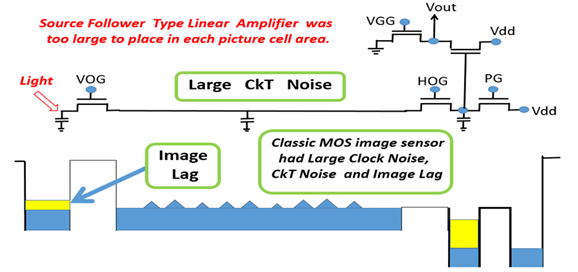
昔の古典的な MOS 型のimage sensor は one transistor 型で
その回路構成は one transistor 型の DRAM メモリセルとほぼ
同一です。もと IBM の R. H. Dennard が1966年に発明した
回路です。この回路は、その後 1969年に Honeywell社の
Bill Regits が考案発明した、信号蓄積容量に直接連結された、
プリアンプ増幅回路( 容量電圧を大電流出力に変換する回路で、
MOS transistor 型の Source follower 回路 )がついていません。
そのため、 one transistor 型は、信号増幅の手段がたいへん
難かしいものでした。Intel社はBill Regits 発明の方式を選びました。
The classical MOS image sensor was one transistor type which
was identical to the one transistor DRAM cell invented by R. H.
Dennard (IBM1966), which did not have any signal preamplifier
circuits, which was proposed by Bill Regits (Honeywell1969).
そして、この one transistor 型DRAM セルは、MOS Transistor型
の電荷転送電極 (charge transfer gate ) を介して、長くてかつ
配線容量が大きな垂直出力信号線に連結されており、その垂直
出力信号線には大きな CkT 雑音が存在し、その為、昔の古典的
な、one transistor type の MOS image sensor は CCD image
Sensor と比較してあまり魅力的ではありませんでした。
And this one transistor DRAM cell was connected directly
to the long output signal line of a very large wire capacitance,
which gave a large CkT noise. So the classical MOS image sensor
was not attractive.
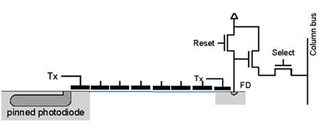
DRAM セルと、 MOS Image Sensor 絵素( picture cell ) は同一です。
DRAM cell and MOS image sensor cell are identical.
MOS 型の Image Sensor の開発歴史は、
DRAM cellの開発史に順応したものです。
The history of the MOS type Image sensor followed closely
the history of the DRAM developments in the past.
One Transistor 型のDRAM Cell が IBMのR. H. Dennardにより
1969年に発明され、その後に 1969年にHoneywell社のBill Regits が
Three Transistor 型のDRAM Cell を発明しました。
今、まさに、 One Transistor 型のMOS image sensorから、1969年に
Honeywell社のBill Regits が発明した、ThreeTransistor 型の、 Active
CMOS image sensor が採用されることになりました。
これは、 Honeywell社のBill Regits の発明です。
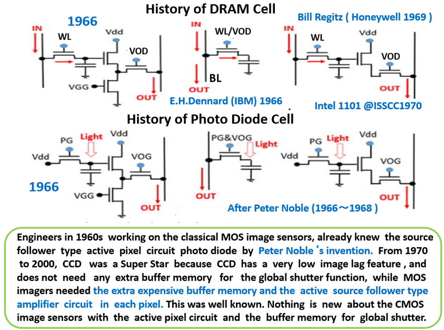
CMOSプロセス技術の微細化が進み、配線容量激減しました。かつ、
MOS transistorの物理的寸法も小さくなりました。 Honeywell 社の
Bill Regitsが 1969年に発明した、この Three Transistor型の Active
Source Follower typeの電流増幅 回路の占める面積も、光感知部、
すなわち、Pinned Photo Diode が占有する、各絵素の面積と比べて、
はるかに、占める割合が小さくなりました。
As the CMOS process scaling down technology advanced, the wire
capacitance was minimized. And also the MOS transistor size
became so small that the area occupied by the three MOS transistor
type preamplifier circuits, invented by Bill Regits ( Honeywell 1969),
could be placed at each light detecting storage area, namely at each
Pinned Photo Diode type light detecting storage area.
その結果、もはや、各絵素に、Source Follower 型の Pre Amp回路を
装備して、Active CMOS image sensor では CkT 雑音の心配は
なくなりました。光感知部 ( Pinned Photo Diode )の小さな信号電荷
の蓄積容量に蓄積された小さな信号電荷が、Source Follower MOS
Transistor の電極と直接連結されることにより、大電流を放出する
ことができるようになったわけで、配線容量のCkT雑音よりはるかに
大きな大電流が出力信号線に流れることになったためです。
The result is, we no longer suffer the CkT noise because the
preamplifier circuits can convert the small signal charge (voltage)
into a very large signal current、much larger than the CkT noise.
One Transistor 型のDRAM Cell が IBMのR. H. Dennardにより
1969年に発明され、その後に 1969年にHoneywell社のBill Regits が
Three Transistor 型のDRAM Cell を発明しました。
今、まさに、 One Transistor 型のMOS image sensorから、1969年に
Honeywell社のBill Regits が発明した、ThreeTransistor 型の、 Active
CMOS image sensor が採用されることになりました。
これは、 Honeywell社のBill Regits の発明です。
Fossum did not invented the three transitor type active CMOS image sensor.
Bill Regits (Honeywell 1969) invented the three transitor type active CMOS
image sensor. Young engineers and students in MOS image sensors in 1970s
all knew this fact, including myself as a CalTech PhD graduate student in 1973.
,
DRAM cell and MOS image senser cell are identical.
Many MOS image sensor engineers knew the Rigitz three
transitor DRAM cell that Intel applied for Intel 1101 DRAM
chip in 1970. The active three transistor circuit for the
CMOS image sensor is the same one Rigits invented in 1969.
Fossum did not invent the active CMOS image sensor.
Hagiwara also knew the active MOS image sensor in 1975
as many other MOS image sensor and DRAM engineers did.
**************************************************************************
CMOS デジカメの開発者は Fossum ではありません。
Pinned Photo Diode の発明者は 寺西さんではありません。
しかし、事実誤認もはなはだしい事が生じ、萩原もSONYもあきれています。
Image Sensor の研究開発の歴史でどうしてこんなひどい事実誤認が
起きたのか、萩原もSONYの技術者も理解に苦しんでいます。
*************************************************************************************
http://qeprize.org/winner-2017/
https://en.wikipedia.org/wiki/Queen_Elizabeth_Prize_for_Engineering
*************************************************************************************
On 1 February 2017, it was announced that the 2017 prize would be awarded
to the four engineers responsible for the creation of digital imaging sensors.
The announcement was made by Lord Browne of Madingley at the Royal Academy
of Engineering, in the presence of HRH The Princess Royal.
The winners of the 2017 prize were:
(1) George E. Smith of United States for the invention of the charge-coupled device (CCD) principle
(2) Michael Tompsett of UK for the development of the CCD image sensor,
including the invention of the imaging semi-conductor circuit and the analogue-to-digital converter
(3) Nobukazu Teranishi of Japan for the invention of the pinned photodiode (PPD)
(4) Eric Fossum of United States for developing the CMOS image sensor
Together, their innovations allowed for advancements in medical treatments, science,
personal communications and entertainment.
The winners will receive their award in a ceremony at Buckingham Palace later in 2017.
**************************************************************************************
これは Image Sensor の開発の歴史における重大な事実誤認の実態を暴露した内容です。
もうすでに多くのここある技術者から事実誤認であることを求める投書も出現しています。
See ElectronicsStackExchangeSite on What is Pinned Photo Diode ?
もと東京工業大学の松澤名誉教授は、
「この悪の根源である Fossum 2014 論文 を fake である。」とあきれていました。
「どうしてこんなバイアスされたものが論文として採用されたのか、理解できない。」と
おっしゃっていました。
また、image sensor の世界の第一人者で、 ISSCC や IEDMの国際学会などで今でも
ご活躍の、オランダのDelft 大学の教授で、 元 philips 社の Prof. Albert Theuwissen
は 「Fossum からFossum 論文の共著になってくれとの依頼を受けたが、論文内容が、
懐疑的( doubtful ) で、sensitive な内容であるので、共著を断った。」 との話でした。
たいへんな Image Sensor の開発の歴史における事実誤認があったことになります。
CMOS デジカメの開発者は Fossum ではありません。
Pinned Photo Diode の発明者は 寺西さんではありません。
以下、その詳細な技術内容の説明になります。たいへん難しく、複雑な内容となります。
半導体物理学の基礎知識と半導体素子の動作原理にかかわる基礎知識も必要です。
しかし、できるだけ細かく何度も繰り返し、いろいろな側面からの解説に挑戦しています。
興味ある方は、ゆっくり、あせらず、マイペースで、何度も目を通して、理解を深めて
いただければ幸いです。特に image sensor 技術に関わる技術者の皆様にはしっかり
読破して理解を深めていただきたいです。
一般の方々でも、半導体物理と半導体デバイスに興味ある方なら、それなりに直観的に、
「昔はCCDが脚光を浴びていたが、今は CMOS デジカメの方が高性能といわれるが、
どうしてか?もはや市場からCCDデジカメが消えたが、それはどうしてか?」 という質問
につて、自分なりに直感的に何となく理解できたかなあ、と感じていただければ幸いです。
to next Page013