**********************
The AIPS ( Artificial Intelligent Partner System ) Home Page 043
hagiwara-yoshiaki@aiplab.com
Private Communications with Prof. Albert Theuwissen
**********************
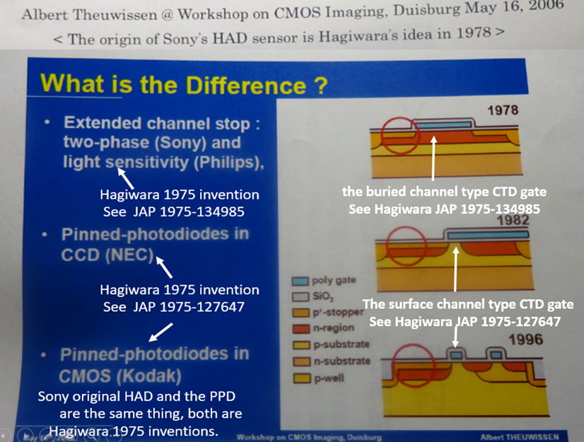
Conclusion : Hagiwara invented the Pinned Photodiode in 1975
in his two Japanese Patents ( 1975-127647 and 1975-134985)
Hagiwara Patent 1975-127647 filed on Oct 22, 1975 defines
a NPN /Sub junction type Pinne Photodiode both with the
built-in Global Shutter Function of a MOS buffer memory
capacitance and also with the Back Light Illumination scheme.
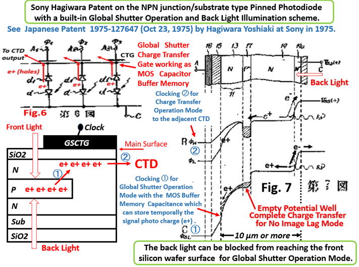
Note the difference from the normal usage of the charge transfer
gate. In this patent claim, the charge transfer gate is also used
as the short-time signal charge storage capacitance as the buffer
memory for the Global Shutter operation scheme. And later by the
second clocking the signal charge is transfered to the adjacent
charge transfer device(CTD). The CTD can be either a CCD type
CTD or a CMOS type CTD with active or passive circuits for each
pixel unit.
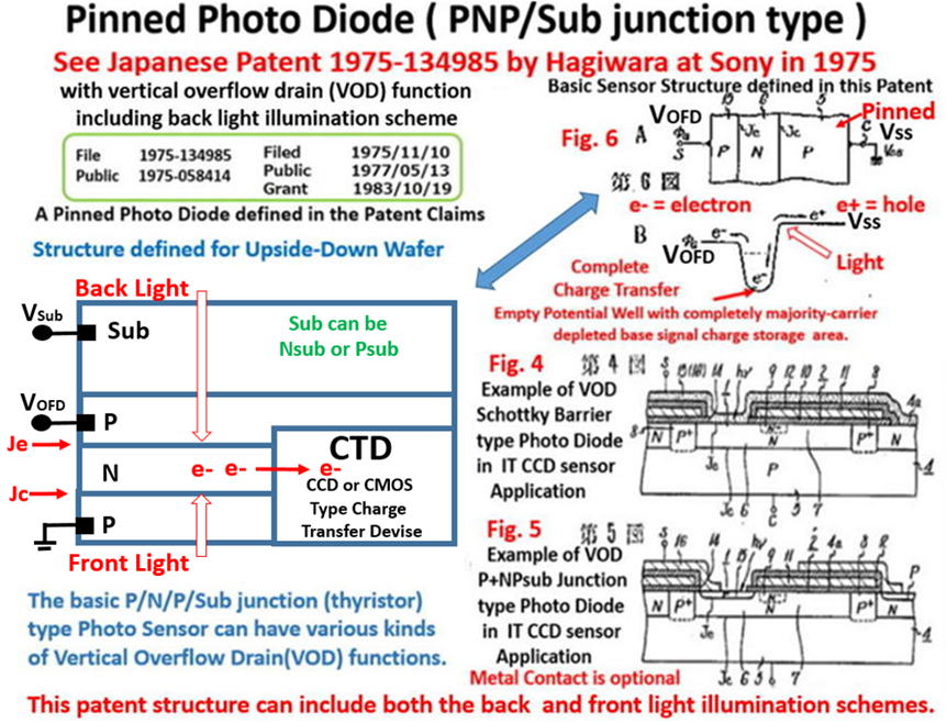
Hagiwara Patent 1975-134985 filed on Nov 10, 1975 defines
a PNP/Sub junction type Pinned Photodiode with the vertical
oveflow drain (VOD) function.
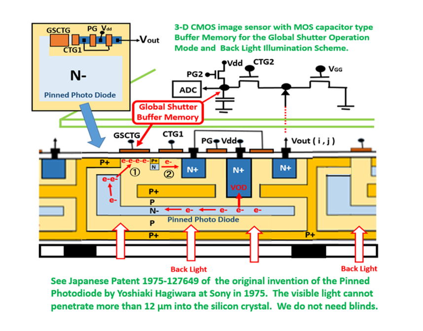
One possbile future application of the Pinned Photodiode.
Note that there are one on-chip P+N junction pinned photodiode buffer
memory and another the second stage buffer memory capacitance for the
double global shutter operations with two reset precharge switch gates.
The very lightly doped PN- junction pinned photodiode is applied as
the photo sensing initial photodiode, and the second fairly lightly doped
PN junction pinned diode is used the first stage buffer memory floating
diffusion for the first stage global shutter scheme. Note also that there
is another second stage global shutter buffer capacitance on the
separate chip before the A/D converter circuit with another second
stage precharge reset switch gate ( Walter Kosonocky invention 1972 )
****************************************************
Private Communications with Prof. Albert Theuwissen
on the invention of Pinned Photo Diode (PPD)
Also see Prof. Albert Theuwissen's blog.
****************************************************
Conclusions:
Peter Noble invented the in-pixel active source-follower
type current amplifier circuit. Fossum did not invent it.
Yoshiaki hagiwara invented the Pinned Photo Diode with
the vertical OFD function. Teranish did not invent it.
Fossum and Teranish are incorrectly attributed to the modern
CMOS image sensor invention and development efforts.
**************************************************
FROM: hagiwara [mailto:hagiwara-yoshiaki@aiplab.com]
SENT: Tuesday, July 10, 2018 3:19 PM
TO: 'a.theuwissen'
SUBJECT: RE: NEC-SONY Patent War
**************************************************
> Hi, Albert,
>
> how are you ?
>
> I am very mad at Fossum's 2014 paper
>
> which I found just a few weeks ago.
>
> I am now 70 years and completely retired..
>
> Fossum did not quote the very important
>
> Pain's work at JPL CalTech
>
>on theGlobal Shutter CMOS image sensor ...
>
> Yoshi
**************************************************
On Tue, 10 Jul 2018 18:24:23 +0900, hagiwara wrote:
> Albert,
>
> I am sorry my previous e-mail title was in Japanese,
>
> copying to many unrelated people.
>
> But they are also my friends.
>
> I am re-sending with more information
> on the Pain's paper.
>
> You know, I was also a visiting professor
> at CalTech during 1998 to 1999
>
> and frequently visiting Pain's Lab at JPL,
> CalTech during the period.
>
> I remember Pain and his team really hated
> Fossum at that time.
>
> I recall they called Fossum a thief.
>
> Kind regards
>
> Yoshi
>
***************************************************
From: albert theuwissen
Sent: Tuesday, July 10, 2018 6:55 PM
To: hagiwara-yoshiaki@aiplab.com
Subject:
Re: How are you ? from Yoshi of Sony(Hagiwara180710)
***************************************************
Dear Yoshi,
Good to hear from you, although it is not all good news
you are sending to me.
Can you tell me the reference of the Pain paper ?
When and where was it published ?
Very interesting information !!
At the time Fossum started to write the overview paper
about the PPD, he asked me to become a co-author
and to help him out with the paper.
After some doubt I declined his invitation,
because I do know that the discussion
about the inventor of the PPD is very sensitive,
and I do agree with you that the structure
you developed is indeed a PPD,
maybe not called that way at that time and
also invented for some other purpose.
But it still remains a PPD !
At Philips, in the late '70s a very similar structure
was implemented in the CCDs, this was before
I joined Philips in 1983.
So yes, there were several p+/n-/p- structures
known by the time that Teranishi issued his patent.
I fully agree to that.
Looking forward to hear from you,
Regards,
Albert.
***************************************************
***************************************************
From: Albert Theuwissen
Sent: Thursday, November 22, 2018 5:48 PM
To: hagiwara-yoshiaki@aiplab.com
Subject: Fwd: I just visited SONYKumamoto Tech Center
***************************************************
Dear Yoshi,
Thanks for your mail.
I remember the discussion during IISW2013
when Mike Tompsett gave a keynote speech.
He owns the patent entitled "Charge-Couple Device Image
Sensor", while his 2 colleagues Boyle and Smith received
in 2009 the Nobel Prize for the invention of the CCD Image
Sensor.
Very much in contradiction, but unfortunately
that is sometimes the way things happen.
What we also very often see is that a major invention is
based on other things that happened around the inventor.
Sometimes the inventor is triggered
by work of others in the same field.
The only advice I can give you :
do not put too much energy in this,
you cannot change history and
it only makes your frustration bigger.
But if I give talks and trainings about image sensors,
including the working principle of PPD,
I ALWAYS refer to (1) your work,
(2) Philips' work (which is more or less a copy of
what you did, but 1 or 2 years later than yours) and
(3) Teranishi's work.
So I do not forget you !!!
I think that the active pixel sensor
with an in-pixel source follower
is described for the first time
by Peter Noble, in 1968
or maybe already in 1966.
He just published a book about his invention.
BTW, I am a bit jaelous on you
because you had the opportunity
to visit the fab of Sony in Kumamoto.
This is one of my dreams
to ever visit the Sony's fab,
including their test facilities.
Wishing you all the best in everything you do !!
Regards,
Albert.
**********************************************************
From: Albert Theuwissen
Sent: Tuesday, November 27, 2018 1:35 AM
To: hagiwara-yoshiaki@aiplab.com
Subject:
RE: the Japanese Official Invention WEB site
**********************************************************
Hi Yoshi,
It is everywhere the same story.
What do you think :
- who invented/developed the stitching technology
for large area image sensors ?
- who owns the world record in low-noise
in the voltage domain for CIS ?
Regards, Albert.
*******************************************************
From: hagiwara [mailto:hagiwara-yoshiaki@aiplab.com]
Sent: Wednesday, February 20, 2019 12:36 PM
To: 'Albert Theuwissen'
Subject:
RE: Please copy to Dr.Nakamura and Dr.Pain
RE: I actually filed in 1975 three Japanese patents (Hagiwara181212)
*******************************************************
Hi, Albert,
Thank you very much for Nakamura-san's e-mail.
I mailed Nakamura-san and he seemed a bit confused ??
I am now explaining Nakamura-san that
In 1975, Hagiwara invented
a P+NPNsub junction type photo-diode,
which is now called in Sony internally
the SONY original HAD sensor.
In 1980, Teranishi-san invented
a P+NPsub junction type buried photo diode
which is identical to the P+NP junction of
the P+NPNsub junction type photo diode
defined as the SONY original HAD sensor.
In 1978, Yamada-san invented
a NPNsub junction type photo diode
with vertical OFD (VOD) function,
which is not a PPD but with VOD,
but identical to the NPNsub junction of
the P+NPNsub junction type photo diode
defined as the SONY original HAD sensor.
The charge is stored in the N region and
to be transferred to the adjacent charge
transfer device with the complete charge
transfer mode resulting the completely
majority carrier depleted N region.
Hagiwara claims that Hagiwara at Sony invented in 1975
the P+NPNsub junction type photo didoe, which is
a thyristor-like structure composed of two transistors.
One is a P+NP junction transistor-like structure and
the other is a NPNsub junction transistor-like structure.
The P+NP junction transistor-like structure is
the 1980 invention by Teranishi-san at NEC.
The NPNsub junction transistor-like structure is
the 1978 invention by Yamada-san at Toshiba.
However, SONY HAD is actually the Pinned Photo Diode
(of a P+NP junction type ) with the VOD function
(by a NPNsub junction).
So, Hagiwara in1975 invented both the PPD and
VODstructures. Am I wrong ?
You wrote me before that
"I remember the discussion during IISW2013
when Mike Tompsett gave a keynote speech.
He owns the patent entitled
"Charge-Couple Device Image Sensor",
while his 2 colleagues Boyle and Smith
received in 2009 the Nobel Prize
for the invention of the CCD Image Sensor.
Very much in contradiction, but unfortunately
that is sometimes the way things happen."
Was the Mike Tompsett CCD patent
before the CCD works of Boyle and Smith ?
Yes, sometimes the inventor is triggered
by work of others in the same field.
This happens a lot in SONY.
In SONY, many diligent engineers including myself
did many works, but the management level people
secretly published important patents after
reviewing our internal company reports.
We did not know the details of their secret patent
applications sometimes after more than ten years.
It was too late for us to speak up.
By the time we noticed, the management level peoples
already received a lot of acknowledgements and
recognition awards inside and also outside of SONY.
The only saver was the opportunity given to us, young
engineers to publish technical papers. But sometimes
by some political reasons, the management people did
not allow the young engineers including myself to publish
our important works, simply because the management people
wanted to establish the mass production technology and
enjoy business quickly before the technical papers exposure
to the competing companies.
Yes, sometimes the inventor is triggered
by work of others in the same field.
As far as I see, this happened a lot in SONY.
But in the case of my 1975 invention, the management
people did not understood the importance of my invention.
I tried and explained often to convince the management
people to allow me to file patents on my idea.
I filed three patents, 1975-134985, 1975-127647 and 1975-127646.
I got Sony permission to apply for the public patent claim
examinationonly on my JAP 1975-134985 patent. SONY
managements did not give permissions to apply for
examinations on my JAP 1975-127647 and JAP 1975-127647.
SONY did not see any importance and abandoned
the patent rights on my inventions of
JAP 1975-127647 and JAP 1975-127647 patents.
SONY managements did not feel the importance an did not
allow me to apply any UPS and other oversea patents
for my inventions including JAP 1975-134985 patent,
that later saved SONY image sensor business from Fairchild,
KODAKand NEC and other competing companies.
I was trying to PR my patent ideas to SONY managements,
but they were already focusing the ILT CCD image sensor
with lateral OFD and transparent electrode type MOS photo
sensor structure with no image lag feature but with a large
surface dark current, which was not a good approach for
CCD image sensor mass production.
But they were optimistic and working very hard.
But they did not understand the physics of semiconductors,
although they were very excellent experts of CCD process
development technology.
Yes, sometimes the inventor is triggered by work
of others in the same field.
But in my case, my idea and invention came first and
then SONY Hagiwara 1978 FT image Sensor work and
NEC Teranishi 1983 ITL image sensor works followed.
So in my case, my invention triggered works of others
in the same field.
So I am still struggling to claim that I am the inventor
of the Pinned Photo Diode which is identical to SONY
HAD sensor of the P+NPNsub junction photo diode
with the VOD function built-in.
Yoshi
***************************************************
**********************
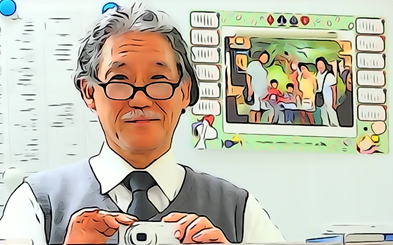
The AIPS image sensor watching at its inventor, Yoshiaki Hagiwara.
return to TOP Page
**********************