**********************
The AIPS ( Artificial Intelligent Partner System ) Home Page 012
**********************
*******************************************************************
In 1960s, before CCD was invented, we already had beautiful color pictures
by the classical MOS image sensor with an excellent light sensitivity obtained
by the classical N+P junction type photo diode.
But to overcome the very large wire (CkT) noise, the three transistor
active source follower type circuits, invented by Peter Noble, was needed.
But the picture cell area was too small to incorporate this active circuit
in each picture cell area. We all knew that we had to wait untill we have
the complete MOS transistor process scale down, much furthur down.
(2) However, the CCD invention gave the image lag free and very low
wire (CkT) noise pictures. The CCD became the super star with the
help of the P+NPNsub junctiion (thyrsitor) type photo diode, which
was invented by Hagiwara in 1975. See JAP ( 1975-134985 ) .
CCD consumed a lot of power with only the transfer efficency of 99.999
%,
which was however possible to be applied for the classical NTSC picture
resolution. CCD had the serious trap noise and surface dark current problems.
Moreover, CCD had inherently MOS metal-type electrodes that do not pass
light and CCD was not as light-sensitive as the N+P photo diode. So, the
CCD
type light detecting picture cell was replaced by the the P+NPNsub junctiion
(thyrsitor) type photo diode, Hagiwara 1975 invention. See JAP ( 1975-134985
) .
In 1978, SONY annouced in New York and Tokyo Press Conferences the world
first CCD image sensor with no image lag, very highly light sensitive,
low trap
noise, low surface dark current features of the PNP junction type photo
diode
sensor pixel structure,Hagiwara 1975 invention. See JAP ( 1975-134985 )
.
At that time, the world already gave up the CCD image development efforts.
SONY was the only company that never gave up. Sony showed the future of
CCD image sesnor applications. The truth is that Hagiwara in SONY was the
only engineer in the world who did not give up. And Hagiwara showed the
future of CCD image sesnor applications. by the P+NPNsub junctiion type
photo diode, Hagiwara 1975 invention. See JAP ( 1975-134985 ) .
So Hagiwara save the CCD by his 1975 invention, which is now called by
another name, the Pinned Photo Diode.
The truth is that CCD was NOT highly light sensitive, NOT low dark current
and NOT trap noise free image sensor structure. The true super star was
not CCD. The true super star was hiden behind the curtain. The true super
star was Hagiwara 1975 invention, which is now called by another name,
the Pinned Photo Diode. SONY called it as the SONY original HAD sensor.
The truth is that the Pinned Photo Diode and the SONY original HAD sensor
are the same thing, that Hagiwara of SONY invented in 1975.
In conclusion, Hagiwara of SONY invented and his team of many dilligent
and hard working SONY engineers developed the stitching technology
for large area image sensors. The world followed after SONY efforts.
(3) Now, the complete CMOS transistor process scale down was achieved.
And the scale-downed three transistor active source follower type circuits,
originally invented by Peter Noble, can be now easily incorporated in each
picture cell of the CMOS image sesnors, with the help of the P+NP junctiion
type photo diode with the back light illumination scheme, which is again
the
invention by Hagiwara in 1975. See JAP( 1975-127647 ).
SONY diligent and hard working engineers developed the modern dgital
CMOS image sensor with the back light illumination scheme for the
first time in the world.
Now again SONY owns the world record in low-noise in the voltage domain
for the modern digital CMOS image sensors (CISs).
Hagiwara 1975 invention ( JAP 1975-134985 ) helped CCD image sensor in
the past.
Hagiwara 1975 invention ( JAP 1975-127647 ) is helping CMOS image sensor
now.
Hagiwara and his original team of SONY diligent and hard working engineers
developed
the stitching technology of both CCD and CMOS large area image sensors.
CCD was considered as the Super Star in the image sensor world in the past,
and the inventors were awarded with the NOBEL prize. But now CCD has
completely dissappeared from the modern digital image sensor world.
So who were the real super stars in the world ?
And now who are the real super stars in the world ?
*******************************************************************
*******************************************************************
Questions by Prof. Albert Theuwissen are ,
- who invented and developed the stitching technology
for large area image sensors ?
- who owns the world record in low-noise
in the voltage domain for CMOS Image Sensor (CIS) ?
*******************************************************************
Hagiwara believes that
Hagiwara invented it , in the Japanese 1975 patent ( 1975-134985 ) as the P+NPNsub
junction ( Thyristor ) type Light Detecting Picture Cell Structure, and Sony diligent
engineers, including Haggiwara, developed, the stitching technology for large area image
sensors. SONY called it as the SONY original HAD sensor technology in SONY business.
Naturally, the technical world did not use the SONY businesss Brand Name HAD, and
called it by another name, the Pinned Photo Diode. But the Pinned Photo
Diode and
SONY original HAD are the same thing, both invented by Hagiwara in 1975.
At least, Teranishi did not invent the Pinned Photo Diode.
Hagiwara is the inventor of the Pinned Photo Diode.
Sony diligent engineers developed and now Sony owns
the world record in low-noise in the voltage domain for CMOS Image Sensor
(CIS)
with the Pinned Photo Diode with the Back Light Illumination, that was
also invented
by Haiwara of SONY in 1975 the Japanses 1975 patent ( 1975-127647 ).
At least, Fossum is not the inventor of the active image sensor picture
element.
Peter Noble is the inventor of the active image sensor picture element.
http://www.pjwn.co.uk/
In the Fossum 2014 fake paper, Fossum attacked Hagiwara 1975 patent with lies,
insulting Sony and Hagiwara honor and pride on purpose. I could not understand
Fossum motivation. But I am now convinced that Fossum wanted Fossum himself
to be recognized by the world, with false explanations on Fossum friend Teranishi
as the TRUE inventor of the Pinned Photo Diode,NOT Hagiwara.
Fossum wanted to convince the world that Fossum himself developed the modern
CMOS digital camera. But now I understand that Peter and SONY diligent engineers
including Hagiwara. This is not fair at all. It is all lies. The world should know the truth.
Until last June I did not know what is the Pinned Photo Diode. I knew SONY HAD.
But I did not know myself that SONY HAD and the Pinned Photo Diode are the
same thing. My friends in Sony informed me that Teranish received awards from
Queen Elizabeth and Japanese Emperor as the inventor of the Pinned Photo Diode.
SONY diligent engineers were not happy at all. Maybe, Albert and Peter also felt it
as a bad news ? So I began to study what is Pinned Photo Diode last June.
Then I found the Fossum 2014 fake paper. I became really MAD at Fossum.
Besides, SONY won the SONY-NEC Patent war by Hagiwara 1975 patent
against the Teranishi1979 patent a long time ago. So Teranish should know that
Hagiwara is the inventor even though Teranishi published his work in IEDM1982.
Teranishi work was just a copy of Hagiwara 1975 patents that defined as one
Example case of Interline CCD image sensor with the complete charge transfer
Mode ( no image lag ) P+NPNsub junction type photon detector structure,
which is now called as the Pinned Photo diode.
But it is now more than four years after Fossum 2014 fake paper publication.
I found this fake paper, really too late.
I was very, very late since I do not belong to the image sensor community any more.
Yes, with my interests in the intelligent image sensors included, but my current major
interests are in the AIP ( Artificial Intelligent Partner ) systems, including AI software
and AI digital circuit system applications.
Yes, I try to be calm, but cannot be silent.
I feel that the world should know at least what is the truth.
I don’t think I can change the past history.
But people can learn the truth anytime, now and in future.
Yes, many people contributed.
Their deligence and efforts must be much worth recognitions.
*******************************************************************
http://www.aiplab.com/Hagiwara_at_Sony_is_the_true_inventor_of_Pinned_Photo_Diode.html
http://www.aiplab.com/Story_of_Pinned_Photo_Diode.html
http://www.aiplab.com/
*******************************************************************
**********************
これは70歳じじいのぶつぶつぼやきの独り言でした。
**********************
**********************
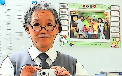
The AIPS image sensor watching at its inventor, Yoshiaki Hagiwara.
return to TOP Page
**********************