**********************
The AIPS ( Artificial Intelligent Partner System ) Home Page 001
**********************
*******************************************************************
Pinned Photo Diode (PPD) and Hole Accumulation Diode (HAD)
PPD and Sony HAD Story
*******************************************************************
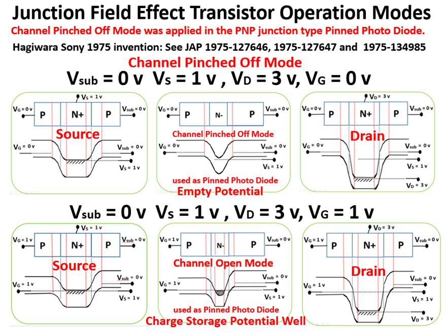
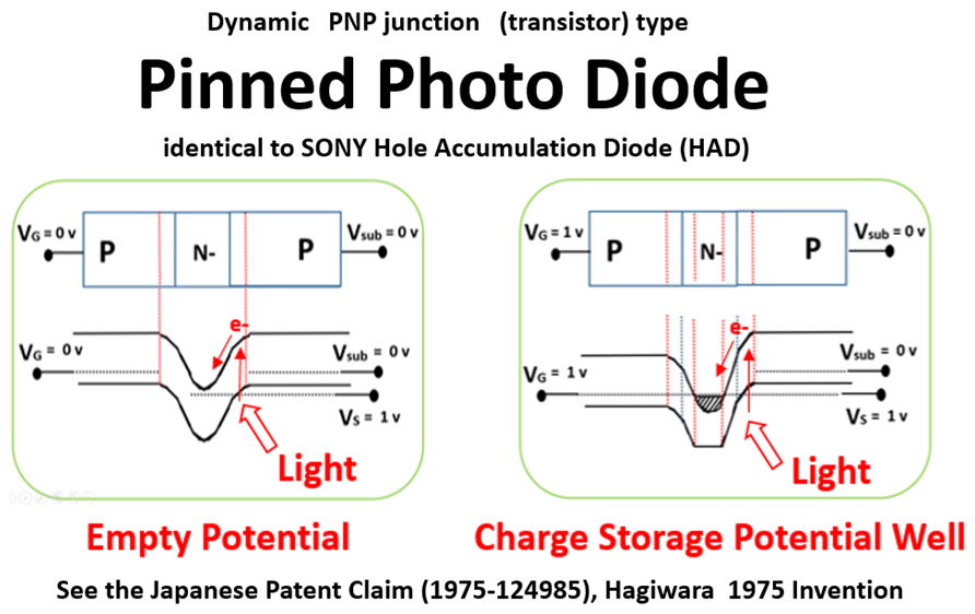
What is the Pinned Photo Diode ? And how does it work ?
You need to understand the concept of the completely depleted base N region
of the PNP junction structure, similar to PNP Bipolar Transistor and also
to
PNP Junction Field Effect Transisor. Study first the structure and operation
modes of Junction Field Effect Transistor (JFET) shown below.
Yoshiaki Hagiwara was invited in the following four international
conferences because of his contributions to the image sensor
community and related digital system LSI chip design works.
See the four invited talks related to the Pinned Photo Diode
which is also called as SONY original Hole Accumulation Diode (HAD)
image sensor. Both Pinned Photo Diode and SONY HAD are identical.
(1) International Conference CCD79 in Edinburgh, Scotland UK
See http://www.aiplab.com/0-CCD79_1979Hagiwara.pdf
(2) International Conference ESSCIRC2001 in Vilach, Austria.
See http://www.aiplab.com/ ESSCIRC2001.pdf
(3) International Conference ESSCIRC2008 in Edinburgh, Scotland UK
See http://www.aiplab.com/ 0-ESSCIRC2008Hagiwara.pdf
(4) International Conference ISSCC2013 in San Francisco, California USA
See http://www.aiplab.com/ ISSCC2013PanelTalk.pdf
(5) Pinned Photo Diode and SONY HAD are the same thing. Both were
invented by Hagiwara at Sony in 1975 in the Japanese Patents
(1975-127646, 1975-127647, 1975-134985).
See http://www.aiplab.com/Pinned_Photo_Diode_1975_invented_by_Hagiwara.pdf
(6) Hagiwara as a PhD student at CalTech designed a Fast 128 bit digital
data stream parallel comparator chip, which was fabricated at Intel
with the Intel 1101 PMOS process technology. Intel 1101 DRAM chip
was based on the Three MOS Transistor type source follower active
current amplifier circuit, which is very similar to the Active Three
MOS Transistor circuit applied to the current CMOS image sensors.
See http://www.aiplab.com/128_bit_Comparator.pdf
(7) Hagiwara designed a Fast 25 nanosecond access time 4 M bit Cache SRAM
chip for digital camera applications. Intel used the SONY SRAM chips in the
Intel boards. Sony enjoyed SRAM business while many companies in Japan
were
focusing on the 4 M bit DRAM chip business.
See http://www.aiplab.com/SONY_4MSRAM_1989.pdf
*******************************************************************
**********************
これは70歳じじいのぶつぶつぼやきの独り言でした。
**********************

**********************
The AIPS image sensor watching at its inventor, Yoshiaki Hagiwara.
return to TOP Page
**********************