**********************
The AIPS ( Artificial Intelligent Partner System ) Home Page 015
**********************
*******************************************************************
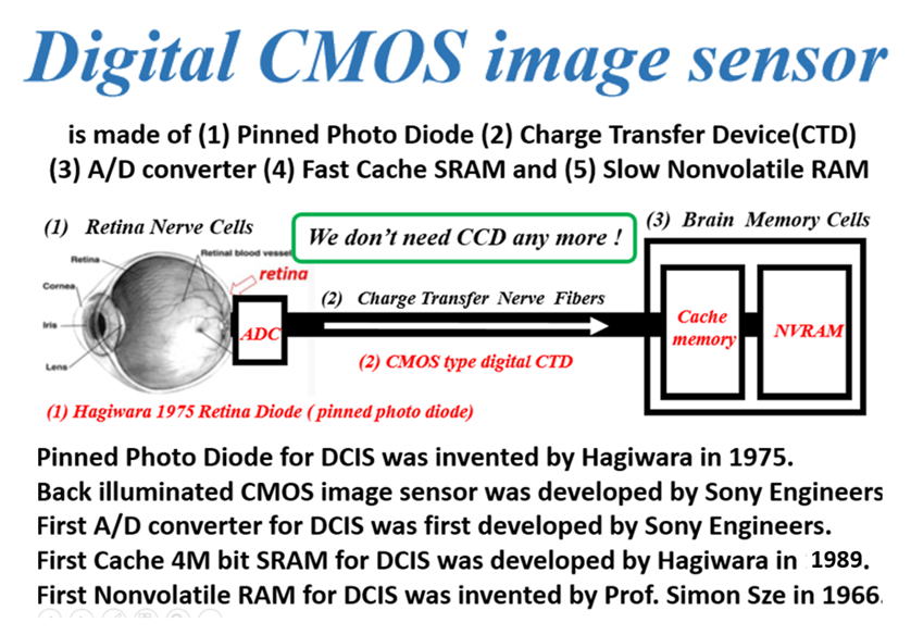
See three invited talks related to SONY HAD sensor now called also as Pinned
Photo Diode.
(1) International Conference CCD79 in Edinburgh, Scotland UK
(2) International Conference ESSCIRC2001 in Vilach, Austria.
(3) International Conference ESSCIRC2008 in Edinburgh, Scotland UK
*******************************************************************
Hagiwara was invited in these international conferences because of his
contributions
to the image sensor community and related digital system LSI chip design
works.
*******************************************************************
However last year Hagiwara learned a very surprising news:
**************************************************************
2017 Queen Elizabeth Prize for Engineering Foundation.
**************************************************************
The winners of the 2017 Queen Elizabeth Prize for Engineering Foundation
were :
(1) George E. Smith for the CCD image sensor invention
(2) Michael Tompsett for the CCD image sensor development.
(3) Nobukazu Teranishi for the invention of the pinned photodiode (PPD)
and
(4) Eric Fossum for developing the CMOS image sensor.
**************************************************************
Hagiwara, the true inventor of the Pinned Photo Diode, got really
surprized at the announcement that Teranishi was awarded for the
invention of the pinned photodiode(PPD), and many SONY dilligent
engineers working for the compact digital CMOS image sensors
got really surprized at the announcement that Fossum was awarded
for developing the CMOS image sensor. The truth is that Teranish
did not invent the PPD. Teranish only developped in 1982 the image
lag free interline CCD image sensor with the PPD light detecting
photo sensor structure that was invented by Hagiwara in 1975.
Hagiwara 1975 patents clearly defined the image lag free interline
transfer CCD image sensor as an application example of his 1975
patent claims.
Fossum wrote a paper on "Active Pixel Sensors: Are CCD's
dinosaurs ?" , in Proc. SPIE, Vol.1900, pp.2-14, 1993. However,
the three transistor type active circuit was already invented by
Bill Regitz of Honeywell in 1969. This active pixel sensors was
not Fossum invention. Fossum actually did not develop the
active pixel sensors either. Sony dilligent engineerings did.
Fossum is not the inventor of the active image sensor picture element
at all.
Peter Noble is the true inventor of the active image sensor picture element.
http://www.pjwn.co.uk/
Hitachi MOS Image Sensor Engineers and Intel MOS Process
Engineers all knew that eventually scaled down MOS Process
Technology will conquer all other kinds of Process Technologies
including CCD image sensor technology because of the power
consideration and scaled down dimensional advantage of CMOS
process technology. The three transistor CMOS active picture
cell was already invented as, since the three-transistor circuit
is identical to, the three-transitor circuit of the DRAM cell with
the active source follower type current amplification. Fossum
was just a commentator in his SPIE 1993 paper above. Fossum
was just emphasizing the well understood fact and speculations
that the original image sensor experts all knew in 1970s. This
active pixel sensors was not Fossum invention.Fossum actually
did not develop the active pixel sensors either.
Sony dilligent engineerings developped the active pixel Pinned
Photo Diode type Light detecting photo sensors for compact
digital CMOS image sensors with the Back Light Illumination.
**************************************************************
*******************************************************************
Questions by Prof. Albert Theuwissen are ,
- who invented and developed the stitching technology
for large area image sensors ?
- who owns the world record in low-noise
in the voltage domain for CMOS Image Sensor (CIS) ?
Hagiwara believes that
Hagiwara invented and Sony diligent engineers developed the stitching technology
for large area image sensors. SONY called SONY original HAD sensor.
But the technical world ignored the SONY businesss Brand Name HAD, and
called it by another name, the Pinned Photo Diode.
Sony diligent engineers developed and now Sony owns the world record in
low-noise
in the voltage domain for CMOS Image Sensor (CIS).
******************************
**********************
これは70歳じじいのぶつぶつぼやきの独り言でした。
**********************
**********************
The AIPS image sensor watching at its inventor, Yoshiaki Hagiwara.
return to TOP Page
**********************