"Story_of_Pinned_Buried_Photodiode_Yoshiaki_Hagiwara_2021_Slid002"Next Slide
...Back Slide
...Slide002.pdf 001..
002..
003..
004..
005..
006..
007..
008..
009..
010.. 011..
012..
013..
014..
015..
016..
017..
018..
019..
020.. 021..
022..
023..
024..
025..
026..
027..
028..
029..
030.. 031..
032..
033..
034..
035..
036..
037..
038..
039..
040.. 041..
042..
043..
044..
045..
046..
047..
048..
049..
050.. 051..
052..
053..
054..
055.. Story_of_Pinned_Buried_Photodiode_Yoshiaki_Hagiwara.pdf Story_of_Pinned_Buried_Photodiode_Yoshiaki_Hagiwara_Part_One.pdf Story_of_Pinned_Buried_Photodiode_Yoshiaki_Hagiwara_Part_Two.pdf Part_One_En_(Slide001-035)
....Part_Two_En(Slide036-055) Part_One_Jp_(Slide001-035)
....Part_Two_Jp(Slide036-055)
https://www.seizansha.co.jp/ISBN/ISBN978-4-88359-339-2.html https://www.seizansha.co.jp/
https://www.seizansha.co.jp/ISBN/ISBN978-4-88359-339-2.html https://www.seizansha.co.jp/ Yoshiaki_Hagiwara_Bio.pdf ........................................
"The Influence of Interface States on Incomplete Charge Transfer in Overlapping Gate Charge Coupled Devices"
"Charge Transfer of Buried Channel Charge Coupled Devices"
"Final Stage of the Charge Transfer Process in Charge Coupled Devices"
Caltech_1975_PhD_Thesis_by_Yoshiaki_Daimon_Hagihara.pdf
Japanese Patent Application JPA1975-127646
Japanese Patent Application JPA1975-127647
Japanese Patent Application JPA1975-134985
"128-Bit Multi Comparator"
P1977_Narrow_Cahnnel_Transfer_Gate_CCD_SSDM1977_Paper_by_Hagiwara.pdf"
Japanese Patent Application JPA1977-126885
Hagiwara_SSDM1978_Paper_on_Pinned_Buried_Photodiode.pdf
"ADVANCES in CCD Imager " Technical Digest of IEEE
IEEE ECS1980 invited paper on "A CCD color imager with narrow-channel transfer gates"
Technology Book on "CCD Image Sensor and Applications"
"A 25-ns 4-Mbit CMOS SRAM with Dynamic Bit-Line Loads"
IEEE1996_Review_Paper_on_Sony_1980_One_Chip_FT_CCD_Image_Sensor
"Sony Semiconductor History"
"DRAM/SRAM Technology and Problem.pdf"
"Micro-Electronics for Home Entertainment"
Turorial Short Cource on Image Sesnors by Yoshiaki Hagiwara.pdf
"SOI Design in Cell Processor and Beyond"
Invited Plenary Panel Talk at ISSCCC2013 on Feb. 2013 on Image Sensors
"The p-n-p-n Diode in Future Linear Motor Cars and in Modern Imagers"
Japanese Patent Application JPA2014_135497
"Design of Time to Frequency Domain Discrete Fourier Transfer Hardware Engine and its performance estimation"
"Digital Frequency Transformation Circuit for Time-wise Unequally Sampled Data"
IEEE_CoolChips_2017_Conference_Invited_Panel_Talk_on_Intelligent_Image_Sensor_Systems.pdf
"Multichip CMOS Image Sensor Structure for Flash Image Acquisition"
"Simulation and Device Characterization of the P+PN+P Junction Type Pinned Photodiode and Schottky Barrier Photodiode"
Japanese Patent Application JPA2020-131313
"Electrostatic and Dynamic Analysis of P+PNP Double Junction Type
http://www.sciencepublishinggroup.com/journal/paperinfo?journalid=245&doi=10.11648/j.ijssam.20210602.13 http://icmts.if.t.u-tokyo.ac.jp/home http://isscc.org/ http://isscc.org/ https://www.coolchips.org/ https://www.coolchips.org/ https://www.caltech.edu/ https://www.gunma-u.ac.jp/ https://www.sojo-u.ac.jp/ http://www.aiplab.com// http://www.ssis.or.jp/ Sony_vs_Loral_Patent_War_1_Reviews.pdf Sony_vs_Loral_Patent_War_2_Supporting_Opinions.pdf E-mail_Communication_on_Sony_Loral_Patent_War_1996.pdf E-mail_communication_with_Albert_san_2018_07_10.pdf HAD_sensor_NEC_SONY_Patent_War.pdf JP1980_138026_NEC_Buried_Photodiode_Patent.pdf JP1978-1971_Toshiba_Yamada_VOD_patent.pdf Sony_vs_Loral_PAtent_War_13_pages.pdf Sony_vs_Loral_Patent_War_53_pages.pdf Image_Sensor_Story_by_Hagiwara.pdf The_evidence_that_Hagiwara_is_the_inventor_of_Pinned_Photodiode_7_pages.pdf Future_of_Image_Sensors_and_Solar_Cells.pdf JP1975-127646_NPNP_triple_junction_Pinned_Photodiode_Patent_32_pages.pdf The_First_Pinned_Photodiode_was_invented_in_1975_by_Yoshiaki_Hagiwar_at_Sony.pdf JP1975-127647_NPN_double_junction_Pinned_Photodiode_Patent_22_pages.pdf JP1975-134985_PNP_double_junction_Pinned_Photodiode_on_Nsub_Patent_7_pages.pdf JP1977-126885_Elecric_Shutter_Clocking_Scheme_by_OFD_Punch_Thru_Action_13_pages.pdf JP2014-135497_Digital_Transformation_Circuit_for_Image_Sensors_29_pages.pdf JP2020_131313_on_Doubel_Junction_Pinned_Photodiode_Solar_Cell_65_Pages.pdf P1978_Pinned_Photodiode_1978_Paper_by_Hagiwara_7_Pages.pdf P1996_Pinned_Photodidoe_used_in_Sony_1980_FT_CCD_Image_Sensor_9_Pages.pdf P2001_ESSCIRC2001_Micro-Electronics_for_Home_Entertainment_11_pages.pdf P2008_ESSCIRC_2008_SOI_Design_in_Cell_Processor_and_Beyond_7_pages.pdf P2013_ISSCC2013_Panel_Talk_25_pages.pdf P2017_CoolChips_Panel_170419_29_pages.pdf P2019_3DIC2019_Paper_on_3D_Pinned_Photodiode_6_pages.pdf P2020_EDTM2020_PaperID_3C4_by_Hagiwara_4_pages.pdf P2021_IJSSA2021_Paper_20210616_on_Electrostatic_and_Dynamic_Analysis_of_Pinned_Photodiodes.pdf Buried_Photodiode_is_not_always_PPD_Hagiwara_Nov_2020.pdf Caltech_1975_PhD_Thesis_Yoshiaki_Daimon_Hagihara.pdf Difference_of_Buried_Photodiode_and_Pinned_Photodiode.pdf E-mail_Communication_on_Sony_Loral_Patent_War_1996.pdf E-mail_communication_with_Albert_and_Yoshi.pdf E-mail_communication_with_Albert_san_2018_07_10.pdf E-mail_communication_with_Albert_san_2018_07_10A.pdf E-mail_communication_with_Albert_san_2018_07_10B.pdf Evidence_that_Hagiwara_is_the_inventor_of_Pinned_Photodiode_2020_10_04a.pdf Evidence_that_Hagiwara_is_the_inventor_of_Pinned_Photodiode_in_Japanese.pdf Future_of_Image_Sensors_and_Solar_Cells .pdf Hagiwara_at_Sony_invented_in_1975_and_developed_Pinned_Photodiode_in_1978.pdf http://www.aiplab.com 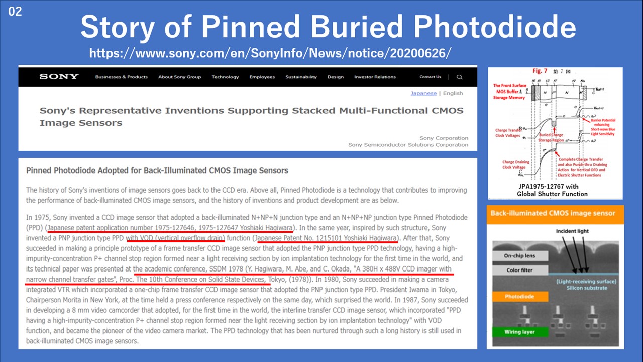
.jpg)