**************************************************
“Story of Image Sensor, Intelligent Electric Eye” Slide 31
**************************************************
++++++++++++++++++++++++++++++++++++++++
“Story of Image Sensor, Intelligent Electric Eye” Slide 31
+++++++++++++ Yoshiaki Hagiwara +++++++++++++++
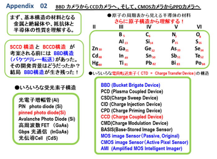
Appendix 02 の説明に入ります。
まず原子の周期表から見える半導体の材料、
さらに原子構造から、いろいろな基本構造
の元となる材料、金属と、絶縁体や、抵抗体
や半導体の性質を理解する必要があります。
過去にいろいろな電荷転送装置、
charge transfer deviceが存在しました。
大昔は、 Bucket Brigate Device と
いうものがありました。
単純にMOSトランジスタを並べているだけです。
Source領域 と drain 領域の
N+P接合が容量Cになります。
それにMOSトランジスタのスイッチが
一列に交互に連結され、並んだものです。
これは電荷転送装置とは呼べない程、
非常に転送効率が悪いでした。
2回か3回ぐらいならOKですが、
それ以上の転送では信号電荷の損失は
無視できませんでした。
1969年にCCDは発明され、1000回転送しても、
電荷がまだ99%保持できたことは、アナログ TV
時代には充分でした。
しかしデジタルTVでは10000回電荷転送が
必要でこれではCCDではもやはや役に
立たなくなりました。
今は CMOS Image Sensor や AMI というもの、
Amplified MOS Intelligent Imager が電荷転送装置が
主流となりました。
イメージセンサーには2つの重要な部品で
構成されていると説明しました。
電荷転送装置に対して、もう一つの
重要な部品は、受光素子です。
受光素子は、1975年の萩原の発明から
今でも受光素子は、同じものが45年間
使われています。しかしそれが本当の
超感度ビデオカメラの正体であることは
あまり理解されていません。
これが本当の超感度カメラの正体です。
P+チャネルSTOP領域がそばに必ず隣接し、
受光部表面のP+層をピン止めGND電圧に
固定したP+NPN接合型の、残像のない、
VOD機能付きの Pinned Photodiodeの
発明でした。
この 残像のない、Pinned Photodiodeは、
また唯一、電子 shutter 機能を可能にする
受光素子でした。
この発明により、固体撮像素子は、
フィルム文化とメカ文化か世界を開放し、
新しい メカ FREEで FILM FREE にして
映像文明に革新をもたらしたことになります。
++++++++++++++++++++++++++++++++++++++++++
Next Page Slide 32
++++++++++++++++++++++++++++++++++++++++++
Slide 01 02 03 04 05 06 07 08 09 10 11 12 13 14 15 16 17 18
Slide 19 20 21 22 23 24 25 26 27 28 29 30 31 32 33 34 35 36
++++++++++++++++++++++++++++++++++++++++++