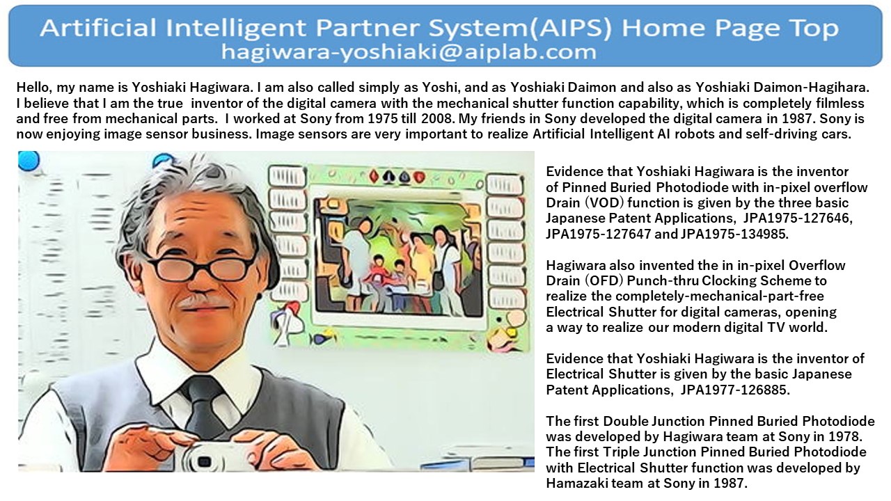
**************************************************
“Story of Image Sensor, Intelligent Electric Eye” Slide 07
**************************************************
++++++++++++++++++++++++++++++++++++++++
“Story of Image Sensor, Intelligent Electric Eye” Slide 07
+++++++++++++ Yoshiaki Hagiwara +++++++++++++++
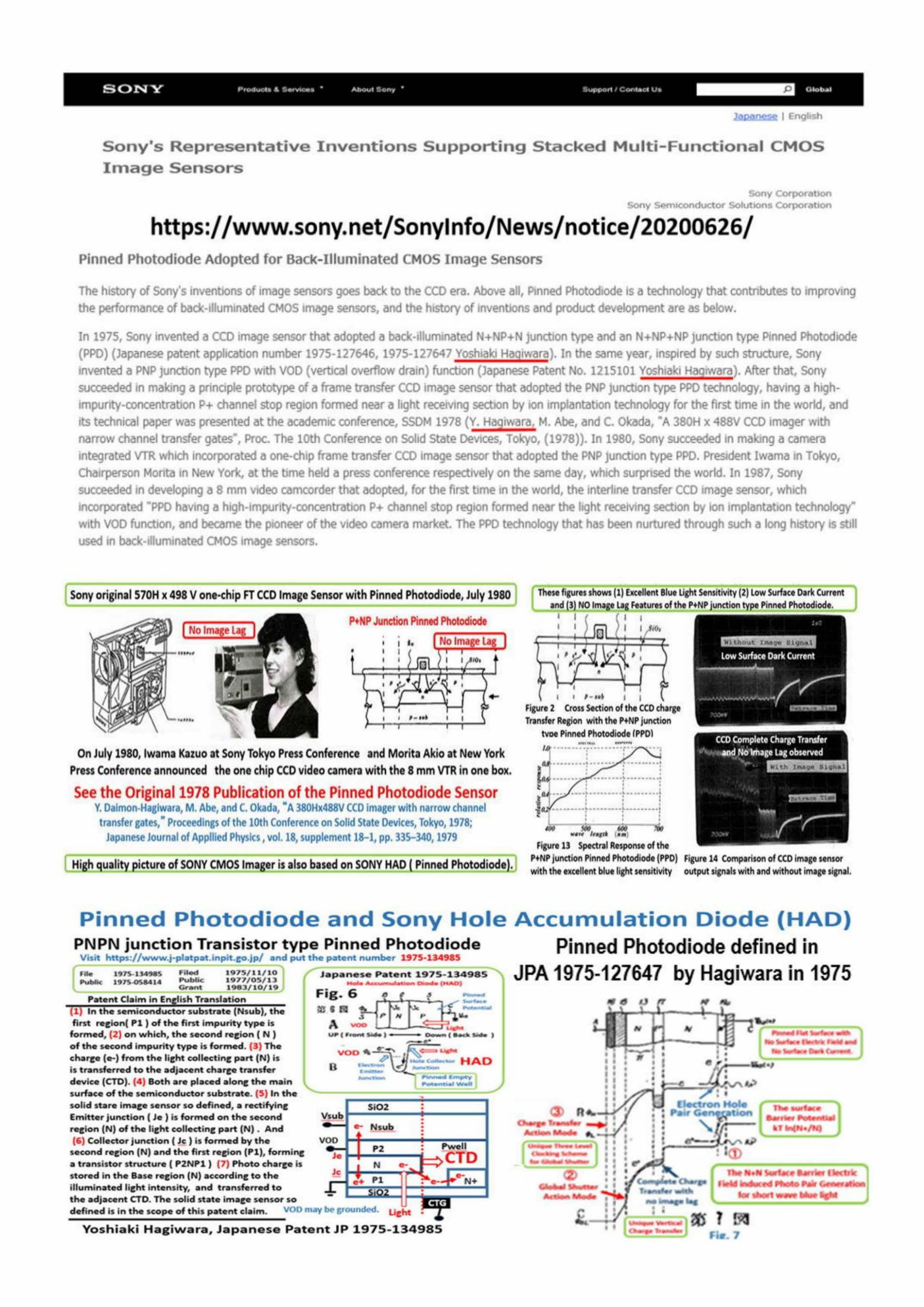
イメージセンサーの開発の歴史の中で、
一番重要なのは、感度です。
イメージセンサーは感度が命です。
このスライドは、1978年ソニーが 380H ×498 V の
フレームトランスファー型イメージセンサーを、
世界初の超感度受光素子、P+NP接合型 Pinned Photodiode、
後にソニーは Hole Accumuation Diode (HAD) と呼んだもの
ですが、それを採用したものが、1978年に東京で開催された、
応用物理学会主催の1978年度の国際学会固体素子 Conference
1978年で、萩原・阿部・岡田の3名の名前で、世界ではじめて、
このP+NP接合型 Pinned Photodiodeに関する、original 論文を
発表しました。
低表面暗電流特性を持ち、短波長光感度が大きく、
雑音が少なく、残像のない映像を実現しました。
配線容量とClock雑音が大きい、当時のMOS型ビデオカメラを、
大きく引き離す結果となりました。
2年後 1980 年7月には、世界初のワンチップのCCDビデオ
カメラをソニーは、東京では岩間社長が、ニューヨークでは
盛田会長が同時に、大々的に新聞発表しました。
超光感度、Hole Accumulation Diodeの新聞発表でしたが、
残念ながら超感度の主役はCCDと誤解されることに
なりました。
571H×498 Vの ワンチップの Frame Transfer 型の
カラーCCDイメージセンサーの実現として理解され、
超感度受光素子の発明には関心がありませんでした。
この構造に採用されたのが、超感度受光素子の、
受光面が隣接する、高濃度の P+ Channel Stops
領域に直接接続された、P+NP接合型の、Hole
Accumulation Diode (HAD) です。
P+NP接合型の、Hole Accumulation Diode (HAD)とは、
受光面がGND電圧に固定、ピン止めされた、Pinned
Photodiodeです。
埋込み型の信号電荷蓄積層、N層を持ちます。
表面の受光面にはP+の濃い Hole Accumulation 領域
があり、その横には、P+の濃い、チャネルストップ
が隣接することがその条件になります。
++++++++++++++++++++++++++++++++++++++++++
Next Page Slide 08
++++++++++++++++++++++++++++++++++++++++++
Slide 01 02 03 04 05 06 07 08 09 10 11 12 13 14 15 16 17 18
Slide 19 20 21 22 23 24 25 26 27 28 29 30 31 32 33 34 35 36
++++++++++++++++++++++++++++++++++++++++++