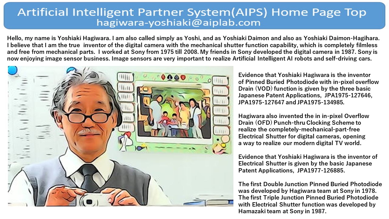
**************************************************
“Story of Image Sensor, Intelligent Electric Eye” Slide 11
**************************************************

++++++++++++++++++++++++++++++++++++++++
“Story of Image Sensor, Intelligent Electric Eye” Slide 11
+++++++++++++ Yoshiaki Hagiwara +++++++++++++++
1975年、私はまだ若い技術者の頃は、
表面照射型タイプ(1)の構造が
主流でした。
受光面といろいろな配線層、wiring layer とか、
信号の処理回路が含んだ、シリコン面を、
主面といいますが、受光面とその主面が
当時は同じシリコンの表面に存在しました。
この場合は、イメージセンサーに入る
受光面積が狭く、感度が悪いでした。
そこで、光ガイド構造、レンティキュラ
構造を使って、集光性を高めました。
しかしそれでもまだ、主面と受光面は
同じ面にあり、配線領域の wiring layer
とは横並びになっていました。
まだ集光率が100%とは程遠いでした。
2000年になり、裏面照射型の、主面と
受光面が、シリコン wafer の反対面に
構成する技術が実現しました。
この裏面照射型の実現に伴い、Two Chip
を貼りあわせる技術が加速進歩しました。
画素部と信号処理回路部、受光面と主面を、
それぞれ別々の2枚のシリコン基板に形成し、
2枚を高精度に位置合わせし、張り合わせて、
その後両方のシリコン基板を、いろんな点で
複数の点で、電気的に接合すコンタクトを
形成するという神業を、ソニーの梅林・
高橋・庄司さん達が考案・開発しました。
シリコンに深い穴を、垂直に井戸を掘る様に、
掘り進み、Cupper金属を埋めるという、
すごい技術を確立しました。
これにより画素部の直下に広い信号処理
領域を確保することができました。
裏面照射型CMOSメジャーの高画質な
基本性能を損なわずに小型化と多様化を
同時に実現することができました。
一階建てのシリコン半導体素子を,
ニ階建てにしたわけです。
実際これで何枚のシリコンチップを
張り合わせが可能となり、三次元
集積回路が実現することになる。
++++++++++++++++++++++++++++++++++++++++++
Next Page Slide 12
++++++++++++++++++++++++++++++++++++++++++
Slide
01
02
03
04
05
06
07
08
09
10
11
12
13
14
15
16
17
18
Slide
19
20
21
22
23
24
25
26
27
28
29
30
31
32
33
34
35
36
++++++++++++++++++++++++++++++++++++++++++
************************************************************
Hagiwara at Sony invented Pinned Photodiode in 1975
index000_Invention_of_Pinned_Photodiode_in_1975.html
index001_Image_Sensor_1975_1977_and_2014_Patents.html
index002_Facts_on_Invention_of_Pinned_Photodiode.html
index003_Hagiwara_Publication_List.html
index004_My_Wonderful_Memory_Pictures.html
index005_Image_Sensor_Story_by_Hagiwara.html
index006_Slide_Sony_Atsugi_Tech_2020_07_10.html
*************************************************************
*********************************************************************
http://www.aiplab.com/index_Page001_E_Tegami.html
http://www.aiplab.com/index_Page002_Waka.html
http://www.aiplab.com/index_Page003_Enoy_Hungle.html
*********************************************************************
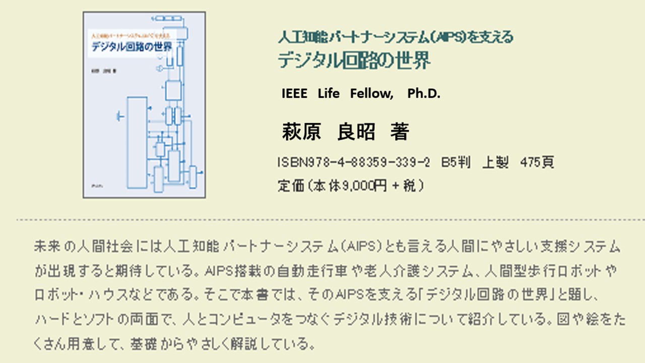
Yoshiaki Hagiwara wrote a book on
"the World of Artificial Intelligent Digital Circuits",
which is important and needed to built
the intelligent image sensor systems.
ISBM978-4-88359-339-2
Hard Cover, 460 page,
\ 9000 Japanese Yen + tax
If you are interestied in the book, Please visit
https://www.seizansha.co.jp/ISBN/ISBN978-4-88359-339-2.html
https://www.seizasha.co.jp/
********************************************************
hagiwara-yoshiaki@aiplab.com http://www.aiplab.com/
hagiwara@ssis.or.jp http://www.ssis.or.jp/en/index.html
********************************************************
******************************
Return to Top Page
http://www.aiplab.com/
*********************************