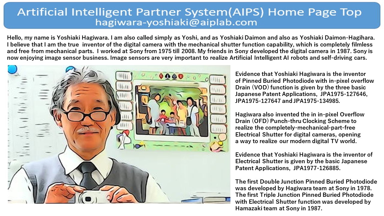
**************************************************
“Story of Image Sensor, Intelligent Electric Eye” Slide 24
**************************************************

++++++++++++++++++++++++++++++++++++++++
“Story of Image Sensor, Intelligent Electric Eye” Slide 24
+++++++++++++ Yoshiaki Hagiwara +++++++++++++++
CCDイメージセンサーよりCMOSイメージ
センサーが有利になった理由は、低消費
電力のCMOSデジタル回路が使えるためです。
CMOSインバータ回路の特性から
その理由が理解できます。
CMOSインバータからの入出力特性を見ますと、
論理しきい値電圧の VT がちょうど、電源
Vddの、ほぼ半分のところに設定することが
可能です。またこのCMOSインバータ回路は、
直観的に、水門モデルを利用することによって
簡単に理解できます。
賢いイメージセンサーを支える技術はこのCMOSと
Bipolar 技術の融合技術です。NPN接合トランジスタ
の動作原理というのは、簡単に言いますと、
mitter側から、元気な自由電子が、丘の上にいる
女の子に跳びつこうとします。
しかし100人の男のが飛びつくんですが、
9人は、そばにある、 collector側の崖に
しくも落ちてしまいます。
100 人中 1 人だけが女の子と結ばれて、
photon、光になるか、または熱になって
消滅します。これが Bipolarトランジスタ
の増幅原理になりますね。
1 人の女の子で 100 人の男の動かすということです。
これが増幅からの原理になります。
現在のCMOS裏面照射型の Image Sensorは
この様に複雑な構造になっています。
それら中に、NやP領域があり、よく見ると、
Bipolarなのか、CMOSなのか、わからない
構造になっています。
かつその上には2枚目のチップには
AD 変換器とかキャッシュメモリ、
さらに3枚目、4枚目となりますと
マイクロプロセッサーとか画像処理
dedicated engine や Cell Processor を
組み込むことが可能になります。
賢い遺伝子の目の開発が進んでいるということですね。
++++++++++++++++++++++++++++++++++++++++++
Next Page Slide 25
++++++++++++++++++++++++++++++++++++++++++
Slide
01
02
03
04
05
06
07
08
09
10
11
12
13
14
15
16
17
18
Slide
19
20
21
22
23
24
25
26
27
28
29
30
31
32
33
34
35
36
++++++++++++++++++++++++++++++++++++++++++
************************************************************
Hagiwara at Sony invented Pinned Photodiode in 1975
index000_Invention_of_Pinned_Photodiode_in_1975.html
index001_Image_Sensor_1975_1977_and_2014_Patents.html
index002_Facts_on_Invention_of_Pinned_Photodiode.html
index003_Hagiwara_Publication_List.html
index004_My_Wonderful_Memory_Pictures.html
index005_Image_Sensor_Story_by_Hagiwara.html
index006_Slide_Sony_Atsugi_Tech_2020_07_10.html
*************************************************************
*********************************************************************
http://www.aiplab.com/index_Page001_E_Tegami.html
http://www.aiplab.com/index_Page002_Waka.html
http://www.aiplab.com/index_Page003_Enoy_Hungle.html
*********************************************************************
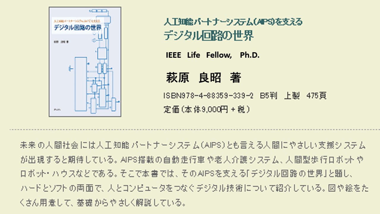
Yoshiaki Hagiwara wrote a book on
"the World of Artificial Intelligent Digital Circuits",
which is important and needed to built
the intelligent image sensor systems.
ISBM978-4-88359-339-2
Hard Cover, 460 page,
\ 9000 Japanese Yen + tax
If you are interestied in the book, Please visit
https://www.seizansha.co.jp/ISBN/ISBN978-4-88359-339-2.html
https://www.seizasha.co.jp/
********************************************************
hagiwara-yoshiaki@aiplab.com http://www.aiplab.com/
hagiwara@ssis.or.jp http://www.ssis.or.jp/en/index.html
********************************************************
******************************
Return to Top Page
http://www.aiplab.com/
*********************************