**************************************************
“Story of Image Sensor, Intelligent Electric Eye” Slide 14
**************************************************


++++++++++++++++++++++++++++++++++++++++
“Story of Image Sensor, Intelligent Electric Eye” Slide 14
+++++++++++++ Yoshiaki Hagiwara +++++++++++++++

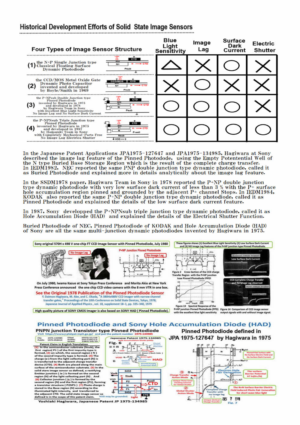
このスライドでは6種類のイメージセンサーと
その6種類の特徴をテーブルにまとめたものです。

1978年には東芝の山田さんが基板にNP接合を
構成する、NPNsub接合型のVOD受光素子を
発明されました。

またNECの寺西さんは基板にPN接合を構成する、
PNPsub接合型の、埋め込み型受光素子を
1980年に発明されました。

この東芝の山田さんのNP接合とNECの寺西さんの
PN接合を合体したものが、P+NP接合構造の
受光素子で、萩原は1975年にP+NPNsub接合型の、
VOD機能付き Pinned Photodiodeの受光素子を
発明しました。

この1975年萩原考案の構造は、山田さんと
寺西さんの両方の受光素子の特性を持ち、
かつ、電子 shutter という、新しい機能までも、
この合体された構造では、可能になりました。

全てがマルになります。電子 shutterというものが
実現するためには、P+表面電位が完全に固定、
ピン止めされた Photodiodeでなければなりません。 

残像のない受光素子でなければ 電子 shutter
として機能しません。

山田さんのN+P接合型受光素子では表面の
電荷蓄積部が浮遊状態ですので、ピン止め
されておらず、残像が生じる場合があり、
電子Shutterとして機能はしません。

また、NECの寺西さん考案の、埋込み型の
PNP接合型受光素子も、受光面が必ずしも、
電圧固定されておらず、ピン止めされていません。

埋込み型Photodiodeは必ずしも Pinned
Photodiodeではありえません。

このNECの寺西さん考案の構造でも、
電子Shutter機能も持たないのは明白です。

実はこの電子 shutter機能の実現が、
ソニーが世界のビデオカメラ市場を
制覇する強力な武器となりました。

ソニーが世界のビデオカメラ市場を
制覇できたのは、超光感度で、
低表面暗電流特性を持ち、かつ、
残像がなく、VOD付きで、かつ、
隣接するP+の Channel Stops 領域で
受光面がピン止めされた P+NPNsub
接合構造が組み込まれ、高速アクション
撮影を可能にした、電子shutter 機能の
Pinned Photodiode だったからです。


++++++++++++++++++++++++++++++++++++++++++
Next Page Slide 15
++++++++++++++++++++++++++++++++++++++++++
Slide 01 02 03 04 05 06 07 08 09 10 11 12 13 14 15 16 17 18
Slide 19 20 21 22 23 24 25 26 27 28 29 30 31 32 33 34 35 36
++++++++++++++++++++++++++++++++++++++++++


************************************************************
Hagiwara at Sony invented Pinned Photodiode in 1975
index000_Invention_of_Pinned_Photodiode_in_1975.html
index001_Image_Sensor_1975_1977_and_2014_Patents.html
index002_Facts_on_Invention_of_Pinned_Photodiode.html
index003_Hagiwara_Publication_List.html
index004_My_Wonderful_Memory_Pictures.html
index005_Image_Sensor_Story_by_Hagiwara.html
index006_Slide_Sony_Atsugi_Tech_2020_07_10.html
*************************************************************

*********************************************************************

http://www.aiplab.com/index_Page001_E_Tegami.html

http://www.aiplab.com/index_Page002_Waka.html

http://www.aiplab.com/index_Page003_Enoy_Hungle.html

*********************************************************************


Yoshiaki Hagiwara wrote a book on
"the World of Artificial Intelligent Digital Circuits",
which is important and needed to built
the intelligent image sensor systems.

ISBM978-4-88359-339-2
Hard Cover, 460 page,
\ 9000 Japanese Yen + tax

If you are interestied in the book, Please visit

https://www.seizansha.co.jp/ISBN/ISBN978-4-88359-339-2.html

https://www.seizasha.co.jp/


********************************************************
hagiwara-yoshiaki@aiplab.com http://www.aiplab.com/

hagiwara@ssis.or.jp http://www.ssis.or.jp/en/index.html
********************************************************

******************************
Return to Top Page
 http://www.aiplab.com/

*********************************