*******************************************************************
Story of Pinned Photo Diode
hagiwara-yoshiaki@aiplab.com
Hagiwara at Sony is the true inventor of Pinned Photo Diode.
See also ElectronicsStackExchangeSite on What is Pinned Photo Diode ?
*******************************************************************
Pinned Photo Diode was invented by Hagiwara of Sony in 1975
Return to The AIPS ( Artificial Intelligent Partner System ) Home Page
Top :
http://www.aiplab.com
*******************************************************************
Brief History of Image Sensors.
*******************************************************************
In 1960s, before CCD was invented, we already had beautiful color pictures
by the classical MOS image sensor with an excellent light sensitivity obtained
by the classical N+P junction type photo diode.
But to overcome the very large wire (CkT) noise, the three transistor
active source follower type circuits, invented by Peter Noble, was needed.
But the picture cell area was too small to incorporate this active circuit
in each picture cell area. We all knew that we had to wait untill we have
the complete MOS transistor process scale down, much furthur down.
(2) However, the CCD invention gave the image lag free and very low
wire (CkT) noise pictures. The CCD became the super star with the
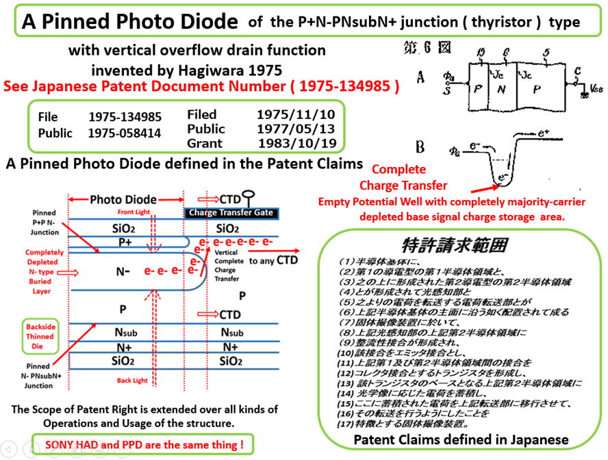
help of the P+NPNsub junctiion (thyrsitor) type photo diode, which
was invented by Hagiwara in 1975. See JAP ( 1975-134985 ) .
CCD consumed a lot of power with only the transfer efficency of 99.999
%,
which was however possible to be applied for the classical NTSC picture
resolution. CCD had the serious trap noise and surface dark current problems.
Moreover, CCD had inherently MOS metal-type electrodes that do not pass
light and CCD was not as light-sensitive as the N+P photo diode. So, the
CCD
type light detecting picture cell was replaced by the the P+NPNsub junctiion
(thyrsitor) type photo diode, Hagiwara 1975 invention. See JAP ( 1975-134985
) .
In 1978, SONY annouced in New York and Tokyo Press Conferences the world
first CCD image sensor with no image lag, very highly light sensitive,
low trap
noise, low surface dark current features of the PNP junction type photo
diode
sensor pixel structure,Hagiwara 1975 invention. See JAP ( 1975-134985 ) .
At that time, the world already gave up the CCD image development efforts.
SONY was the only company that never gave up. Sony showed the future of
CCD image sesnor applications. The truth is that Hagiwara in SONY was the
only engineer in the world who did not give up. And Hagiwara showed the
future of CCD image sesnor applications. by the P+NPNsub junctiion type
photo diode, Hagiwara 1975 invention. See JAP ( 1975-134985 ) .
So Hagiwara save the CCD by his 1975 invention, which is now called by
another name, the Pinned Photo Diode.
The truth is that CCD was NOT highly light sensitive, NOT low dark current
and NOT trap noise free image sensor structure. The true super star was
not CCD. The true super star was hiden behind the curtain. The true super
star was Hagiwara 1975 invention, which is now called by another name,
the Pinned Photo Diode. SONY called it as the SONY original HAD sensor.
The truth is that the Pinned Photo Diode and the SONY original HAD sensor
are the same thing, that Hagiwara of SONY invented in 1975.
In conclusion, Hagiwara of SONY invented and his team of many dilligent
and hard working SONY engineers developed the stitching technology
for large area image sensors. The world followed after SONY efforts.
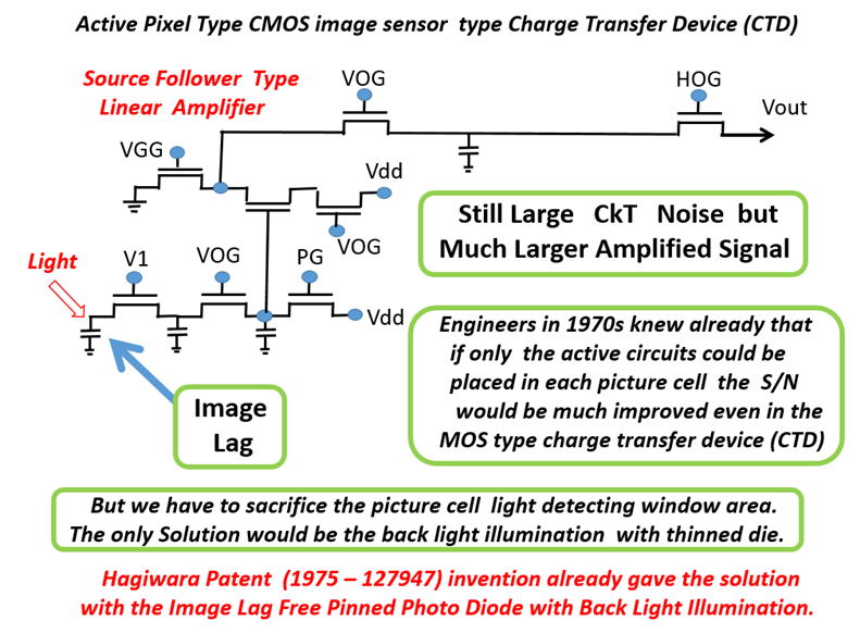
(3) Now, the complete CMOS transistor process scale down was achieved.
And the scale-downed three transistor active source follower type circuits,
originally invented by Peter Noble, can be now easily incorporated in each
picture cell of the CMOS image sesnors, with the help of the P+NP junctiion
type photo diode with the back light illumination scheme, which is again
the
invention by Hagiwara in 1975. See JAP( 1975-127647 ).
SONY diligent and hard working engineers developed the modern dgital
CMOS image sensor with the back light illumination scheme for the
first time in the world.
Now again SONY owns the world record in low-noise in the voltage domain
for the modern digital CMOS image sensors (CISs).
Hagiwara 1975 invention ( JAP 1975-134985 ) helped CCD image sensor in
the past.
Hagiwara 1975 invention ( JAP 1975-127647 ) is helping CMOS image sensor
now.
Hagiwara and his original team of SONY diligent and hard working engineers developed
the stitching technology of both CCD and CMOS large area image sensors.
CCD was considered as the Super Star in the image sensor world in the past,
and the inventors were awarded with the NOBEL prize. But now CCD has
completely dissappeared from the modern digital image sensor world.
So who were the real super stars in the world ?
And now who are the real super stars in the world ?
*******************************************************************
*******************************************************************
*******************************************************************
See three invited talks related to SONY HAD sensor now called also as Pinned
Photo Diode.
(1) International Conference CCD79 in Edinburgh, Scotland UK
(2) International Conference ESSCIRC2001 in Vilach, Austria.
(3) International Conference ESSCIRC2008 in Edinburgh, Scotland UK
*******************************************************************
Hagiwara was invited in these international conferences because of his
contributions
to the image sensor community and related digital system LSI chip design
works.
*******************************************************************
**************************
Story of Pinned Photo Diode
Hagiwara at SONY is the true inventor of Pinned Photo Diode
**************************
See ElectronicsStackExchangeSite on What is Pinned Photo Diode ?
*******************************************************************
See three invited talks related to SONY HAD sensor now called also as Pinned
Photo Diode.
(1) International Conference CCD79 in Edinburgh, Scotland UK
(2) International Conference ESSCIRC2001 in Vilach, Austria.
(3) International Conference ESSCIRC2008 in Edinburgh, Scotland UK
*******************************************************************
Hagiwara was invited in these international conferences because of his
contributions
to the image sensor community and related digital system LSI chip design
works.
*******************************************************************
*******************************************************************
Questions by Prof. Albert Theuwissen are ,
- who invented and developed the stitching technology
for large area image sensors ?
- who owns the world record in low-noise
in the voltage domain for CMOS Image Sensor (CIS) ?
*******************************************************************
Hagiwara believes that
Hagiwara invented it , in the Japanese 1975 patent ( 1975-134985 ) as the P+NPNsub
junction ( Thyristor ) type Light Detecting Picture Cell Structure, and Sony diligent
engineers, including Haggiwara, developed, the stitching technology for large area image
sensors. SONY called it as the SONY original HAD sensor technology in SONY business.
Naturally, the technical world did not use the SONY businesss Brand Name HAD, and
called it by another name, the Pinned Photo Diode. But the Pinned Photo Diode and
SONY original HAD are the same thing, both invented by Hagiwara in 1975.
At least, Teranishi did not invent the Pinned Photo Diode.
Hagiwara is the inventor of the Pinned Photo Diode.
Sony diligent engineers developed and now Sony owns
the world record in low-noise in the voltage domain for CMOS Image Sensor
(CIS)
with the Pinned Photo Diode with the Back Light Illumination, that was
also invented
by Haiwara of SONY in 1975 the Japanses 1975 patent ( 1975-127647 ).
At least, Fossum is not the inventor of the active image sensor picture
element.
Peter Noble is the inventor of the active image sensor picture element.
http://www.pjwn.co.uk/
In the Fossum 2014 fake paper, Fossum attacked Hagiwara 1975 patent with lies,
insulting Sony and Hagiwara honor and pride on purpose. I could not understand
Fossum motivation. But I am now convinced that Fossum wanted Fossum himself
to be recognized by the world, with false explanations on Fossum friend Teranishi
as the TRUE inventor of the Pinned Photo Diode,NOT Hagiwara.
Fossum wanted to convince the world that Fossum himself developed the modern
CMOS digital camera. But now I understand that Peter and SONY diligent engineers
including Hagiwara. This is not fair at all. It is all lies. The world should know the truth.
Until last June I did not know what is the Pinned Photo Diode. I knew SONY HAD.
But I did not know myself that SONY HAD and the Pinned Photo Diode are the
same thing. My friends in Sony informed me that Teranish received awards from
Queen Elizabeth and Japanese Emperor as the inventor of the Pinned Photo Diode.
SONY diligent engineers were not happy at all. Maybe, Albert and Peter also felt it
as a bad news ? So I began to study what is Pinned Photo Diode last June.
Then I found the Fossum 2014 fake paper. I became really MAD at Fossum.
Besides, SONY won the SONY-NEC Patent war by Hagiwara 1975 patent
against the Teranishi1979 patent a long time ago. So Teranish should know that
Hagiwara is the inventor even though Teranishi published his work in IEDM1982.
Teranishi work was just a copy of Hagiwara 1975 patents that defined as one
Example case of Interline CCD image sensor with the complete charge transfer
Mode ( no image lag ) P+NPNsub junction type photon detector structure,
which is now called as the Pinned Photo diode.
But it is now more than four years after Fossum 2014 fake paper publication.
I found this fake paper, really too late.
I was very, very late since I do not belong to the image sensor community any more.
Yes, with my interests in the intelligent image sensors included, but my current major
interests are in the AIP ( Artificial Intelligent Partner ) systems, including AI software
and AI digital circuit system applications.
Yes, I try to be calm, but cannot be silent.
I feel that the world should know at least what is the truth.
I don’t think I can change the past history.
But people can learn the truth anytime, now and in future.
Yes, many people contributed.
Their diligence and efforts must be much worth recognitions.
*******************************************************************
http://www.aiplab.com/Hagiwara_at_Sony_is_the_true_inventor_of_Pinned_Photo_Diode.html
http://www.aiplab.com/Story_of_Pinned_Photo_Diode.html
http://www.aiplab.com/
*******************************************************************
*******************************************************************
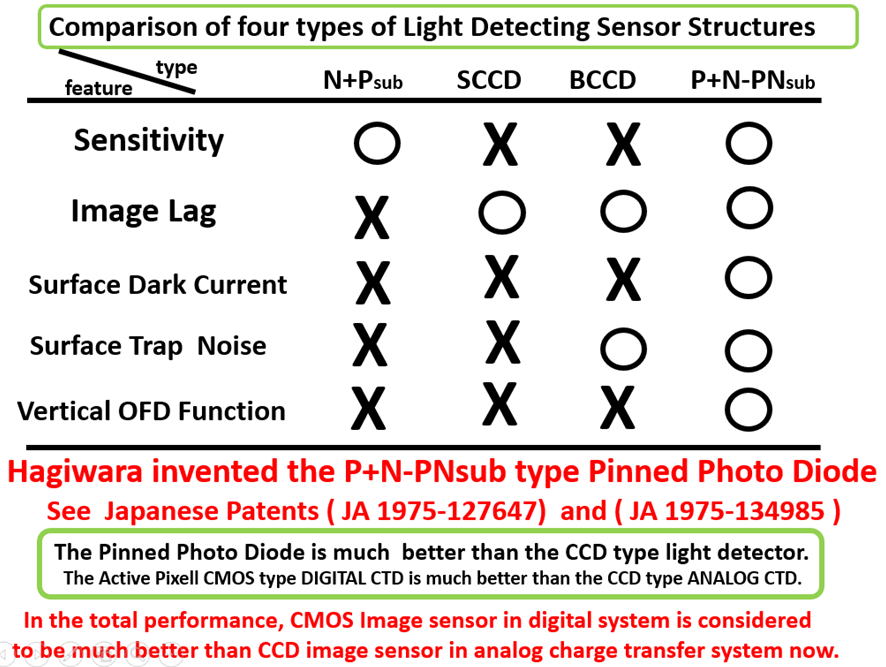
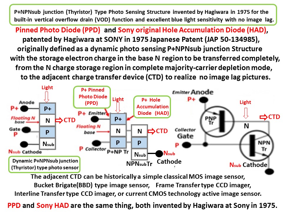
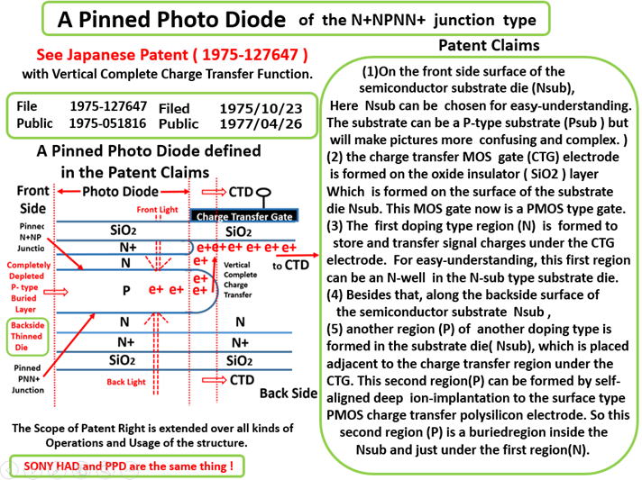
Hagiwara invented the Pinned Photo Diode as shown below.
**************************************************************************
Evidence that Hagiwara at Sony is the true inventor of the Pinned Photo Diode
**************************************************************************
Evidence that Hagiwara at Sony is the true inventor of the Pinned Photo Diode
is given by the two Japanese patents Hagiwara filed in 1975 at Sony. They are,
Japanese Patent (1975-127647) and (1975-134985). The evidence is described in
details in these two Hagiwara 1975 Japanese patents.
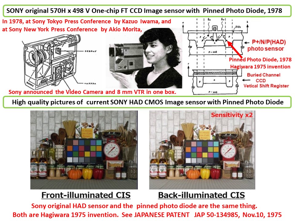
In 1978 Sony announced a new video camera in Tokyo and New York Press
Conferences at the same date, held by Sony Chairman Akio Morita in New York
and Sony President Kazuo Iwama in Tokyo at the same date in 1978.
The video camera announced in the two Press Conference was built with the
Frame Transfer CCD image sensor with the Pinned Photo Diode light detecting
photo sensing picture cell structure that Hagiwara invented in 1975, which has
a very light sensitivity, a very low noise and a very low image lag features.
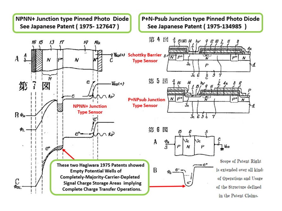
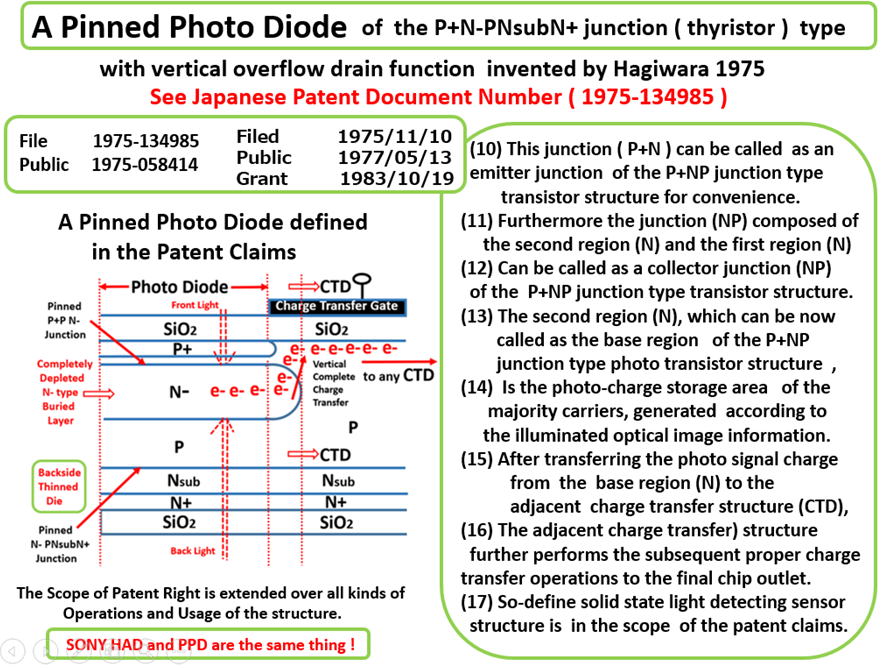
The figures N0.1 thru No.5 in Hagiwara Japanese patent (1975-134985)
explained in details an example of the interline transfer CCD image
sensor application with the Hagiwara invented Pinned Photo Diode.
Sony engineers, after the 1978 Press Conferences in Tokyo and New
York, worked hard for, and succeeded to acquire, the production
and the reliability technolgy of the CCD video camera of the interline
transfer CCD image sensor application with the Pinned Photo Diode
light detecting picture cell structure with the vertical overflow function.
With the diligent SONY engineers efforts, SONY could produce the
portable Passport size Compact CCD image sensor video camera, with
the Pinned Photo Diode that Hagiwara invented in 1975.
And at the same time, Sony filed a trading name officially, which
is the SONY Brand Name of " Sony original HAD sensor " .
With the help of the Hagiwara invented Pinned Photo Diode, which
was now called as " Sony original HAD sensor " with the strong
SONY original sales features of high light sensitivity, low noise and
no image lag characteristics, Sony could become soon very dominant
and strong over the world consumer video camera markets.
The feature of no image lag characteristics in the Hagiwara invented
Pinned Photo Diode is explained and shown in details, as an example
application case, in the figure No.6 of Hagiwara 1975 Japanese Patent
( 1975-134985 ) and also in the figure No.7 of Hagiwara 1975 Japanese
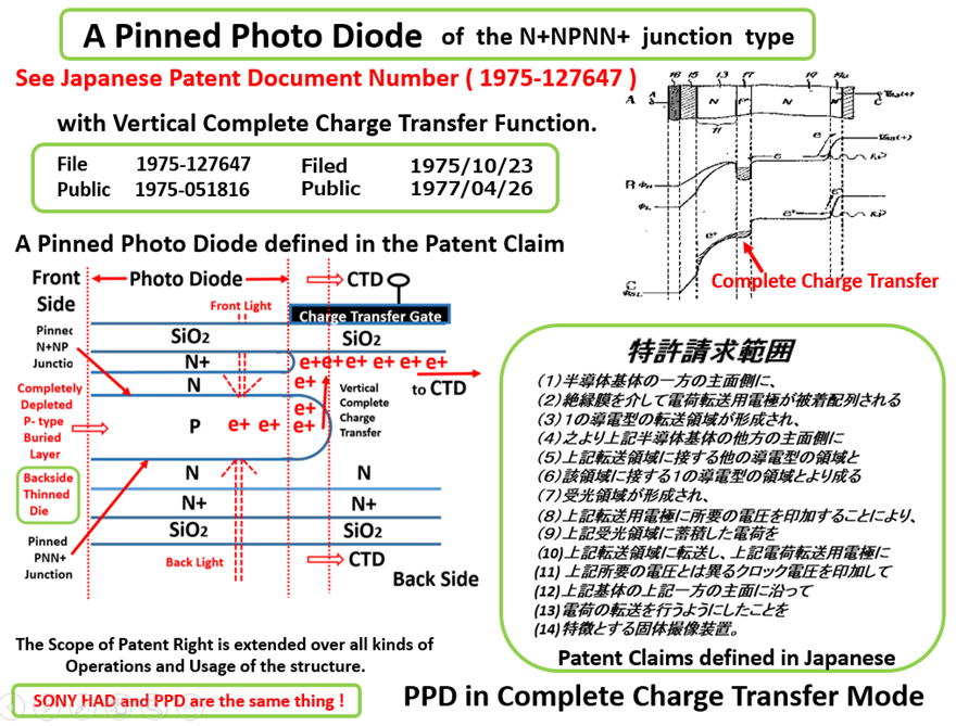
Patent ( 1975-127647 ) in details.
Hagiwara 1975 Japanese Patent ( 1975-127647 ) proposed a Back Light
illumiantion type light detecting photo sensing picture cell structure
with the buried layer type photo signal charge storage. And in the
figure No.7 of Hagiwara 1975 Japanese Patent ( 1975-127647 ) was
shown clearly how the signal charge in the buried storage layer are
trasfered completely to the region under the charge transfer gate
formed on the front side of the silicon wafer. This means clearly
the light sensing picture cell structure, which is now worldly called
as the Pinned Photo Diode, has the very important feature of no
image lag characteristics.
All of these Patent Claim descriptions and Patent figures for possible
patent application examples given in details in the two Hagiwara 1975
Japanese Patents ( 1975-127647 ) and ( 1975-134985 ) support the fact
that Hagiwara is the true inventor of the Pinned Photo Diode.
In conclusion, it is a clear cool fact that Hagiwara at Sony is the true
inventor of the Pinned Photo Diode. The Haiwara patents claims that
the light detecting picture cell structure ( now called as the Pinned
Photo Diode ) can be applied to any kind of charge transfer device(CTD)
which includes the BBD type, the classical MOS type, the CCD type and
the modern CMOS image sensor type charge transfer devices.
Hagiwara proposed the Pinned Photo Diode with the P+NPNsub junction
(thyrisor) type Light detecting picture cell structure with the vertical
over flow drain for the first time in the world.
Moreoever, Hagiwara proposed in the Japanese patent application example
of figure No.7 of Japanse patent (1975-126747) the Back Light illumination
Pinned Photo Diode type Light Detecting Picture Cell Structure for the
first time in the world.
Moreoever, Hagiwara proposed in the Japanese patent application example
of figure No.4 of Japanse patent (1975-134985) the Schottky Barrier type
Light Detecting Picture Cell structure in the Interline transfer type
CCD image sensor applicaiton for the first time in the world.
**************************************************************************
However last year Hagiwara learned a very surprising news:
**************************************************************
2017 Queen Elizabeth Prize for Engineering Foundation.
**************************************************************
The winners of the 2017 Queen Elizabeth Prize for Engineering Foundation
were :
(1) George E. Smith for the CCD image sensor invention
(2) Michael Tompsett for the CCD image sensor development.
(3) Nobukazu Teranishi for the invention of the pinned photodiode (PPD)
and
(4) Eric Fossum for developing the CMOS image sensor.
**************************************************************
Hagiwara, the true inventor of the Pinned Photo Diode, got really
surprized at the announcement that Teranishi was awarded for the
invention of the pinned photodiode(PPD), and many SONY dilligent
engineers working for the compact digital CMOS image sensors
got really surprized at the announcement that Fossum was awarded
for developing the CMOS image sensor. The truth is that Teranish
did not invent the PPD. Teranish only developped in 1982 the image
lag free interline CCD image sensor with the PPD light detecting
photo sensor structure that was invented by Hagiwara in 1975.
Hagiwara 1975 patents clearly defined the image lag free interline
transfer CCD image sensor as an application example of his 1975
patent claims.
Fossum wrote a paper on "Active Pixel Sensors: Are CCD's
dinosaurs ?" , in Proc. SPIE, Vol.1900, pp.2-14, 1993. However,
the three transistor type active circuit was already invented by
Bill Regitz of Honeywell in 1969. This active pixel sensors was
not Fossum invention. Fossum actually did not develop the
active pixel sensors either. Sony dilligent engineerings did.
Fossum is not the inventor of the active image sensor picture element
at all.
Peter Noble is the true inventor of the active image sensor picture element.
http://www.pjwn.co.uk/
Hitachi MOS Image Sensor Engineers and Intel MOS Process
Engineers all knew that eventually scaled down MOS Process
Technology will conquer all other kinds of Process Technologies
including CCD image sensor technology because of the power
consideration and scaled down dimensional advantage of CMOS
process technology. The three transistor CMOS active picture
cell was already invented as, since the three-transistor circuit
is identical to, the three-transitor circuit of the DRAM cell with
the active source follower type current amplification. Fossum
was just a commentator in his SPIE 1993 paper above. Fossum
was just emphasizing the well understood fact and speculations
that the original image sensor experts all knew in 1970s. This
active pixel sensors was not Fossum invention.Fossum actually
did not develop the active pixel sensors either.
Sony dilligent engineerings developped the active pixel Pinned
Photo Diode type Light detecting photo sensors for compact
digital CMOS image sensors with the Back Light Illumination.
**************************************************************
***********************************************
Queston (1)
Why was the CCD image sensor
the super star in the past ?
***********************************************
Question (2)
Why is the CCD image sensor now obsolete
in the modern digital high vision TV era ?
***********************************************
Question(3)
Why is now the CMOS image sensor dominant
over the CCD image sensor ?
***********************************************
***********************************************
Queston (1)
Why was the CCD image sensor
the super star in the past ?
***********************************************
Answer :
The buried channel type CCD has a very high charge
transfer efficiency of 99.999% with very low CkT noise.
In the past TV system of the 720 H x 512 V picture
resolution, we only needed the total of 1232 charge
transfers at most to transfer the signal charge from
the light detecting storage area ( the pinned photo
diode ) to the final chip output buffer circuits.
Therefore, the incomplete charge transfer of
0.001 % x 1232 charge transfer gives 1.232 % of
the total incomplete charge transfer which means
only the 1.232% of image lag and color picture
contamination, which was tolerable in the past
video camera system.
Besides, CCD image sensor has a very low CkT noise,
which is much lower than that of MOS image sensor.
***********************************************
Queston (2)
Why is the CCD image sensor now obselete
in the modern digital high vision TV era ?
***********************************************
Answer :
The buried channel type CCD has very low CkT noise,
but has only a limited charge transfer efficiency of
99.999%, which is now not good enough.
In the modern high resolution TV system, such as in the
4K TV system of the 3840H×2160V picture resolution,
we need the total of 6000 charge transfers at most to
transfer the signal charge from the light detecting storage
area ( the pinned photo diode ) to the final chip output
buffer circuits.
Therefore, the incomplete charge transfer of
0.001 % x 6000 charge transfer gives 6 % of
the total incomplete charge transfer which
means the 6 % of image lag and color picture
contamination, which was not tolerable at all.
Besides, the CCD image sensor consumes
a lot of electric power compared to the
very low power CMOS image sensor.
***********************************************
***********************************************
Question(3)
Why is now the CMOS image sensor dominant
over the CCD image sensor ?
***********************************************
Answer
The classical MOS image sensor was one transistor type which
was identical to the one transistor DRAM cell invented by R. H.
Dennard (IBM1966), which did not have any signal preamplifier
circuits, which was proposed by Bill Regits (Honeywell1969).
And this one transistor DRAM cell was connected directly
to the long output signal line of a very large wire capacitance,
which gave a large CkT noise. So the classical MOS image sensor
was not attractive.
DRAM cell and MOS image sensor cell are identical.
The history of the MOS type Image sensor followed closely
the history of the DRAM developments in the past.
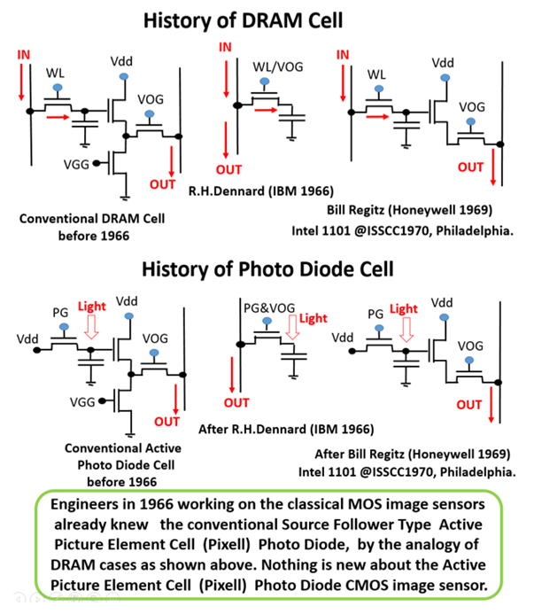
As the CMOS process scaling down technology advanced, the wire
capacitance was minimized. And also the MOS transistor size
became so small that the area occupied by the three MOS transistor
type preamplifier circuits, invented by Bill Regits ( Honeywell 1969),
could be placed at each light detecting storage area, namely at each
Pinned Photo Diode type light detecting storage area.
The result is, we no longer suffer the CkT noise because the
preamplifier circuits can convert the small signal charge (voltage)
into a very large signal current、much larger than the CkT noise.
Fossum did not invented the three transitor type active CMOS image sensor.
Bill Regits (Honeywell 1969) invented the three transitor type active CMOS
image sensor. Young engineers and students in MOS image sensors in 1970s
all knew this fact, including myself as a CalTech PhD graduate student
in 1973.
,
DRAM cell and MOS image senser cell are identical.
Many MOS image sensor engineers knew the Rigitz three
transitor DRAM cell that Intel applied for Intel 1101 DRAM
chip in 1970. The active three transistor circuit for the
CMOS image sensor is the same one Rigits invented in 1969.
Fossum did not invent the active CMOS image sensor.
Hagiwara also knew the active MOS image sensor in 1975
as many other MOS image sensor and DRAM engineers did.
*******************************************************************
Teranishi did not invent the Pinned Photo Diode.
Hagiwara invented the Pinned Photo Diode as shown below.
SONY original HAD and Pinned Photo Diode are the same thing,
both invented and defined in the two Japanese Patents
Please visit the oficial Japanese Patent Search Web Site,
https://www4.j-platpat.inpit.go.jp/eng/tokujitsu/tkbs_en/TKBS_EN_GM101_Top.action
to search Hagiwara's original Japanese Patent and put the following two document number,
Document No. ( 1975-134985 ) on the P+NPNsub junction type PPD Patent
Invention
And
Please visit the oficial Japanese Patent Search Web Site,
https://www4.j-platpat.inpit.go.jp/eng/tokujitsu/tkbs_en/TKBS_EN_GM101_Top.action
to search Hagiwara's original Japanese Patent and put the following two document number,
Document No. ( 1975-127647 ) on the NPNN+ junction type PPD Patent Invention
、
Both were filed by Yoshiaki Hagiwara in 1975 at Sony.
See the original Pinned Photo Diode Patent 1975
The picture shown below gives the image of the large CkT noise generated
in
the long and large-capacitance signal output line.
The CkT noise is just the small movements of water molecules when heated.
The small movements of water molecules is just proportional to the ambient
temperature. And the the total movement energy ( CkT noise ) is proportional
to the capacity ( capacitance ) of the container ( pool ) of the water
molecules.
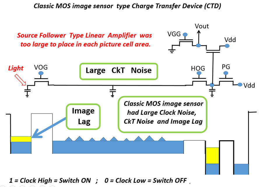
In 1970s, we all knew that we could have a much larger signal output current
if we could place the source follower type preamlifier at each light detecting
picture cell element ( the Pinned Photo Diode ), but we did not do so simply
because the three transistor type source follower preamlifier circuits
was
too large compared to the picture cell light detecting window area. But
now
thans to the drastic scaling down of the MOS transistor dimensions, the
area occupied by the three transistor type source follower preamlifier circuits
became negligible compared to the total area of the picture cell light detecting
window area. Besides, the backlight illumination of the Pinned Photo Diode
which was invented by Hagiwara in 1975 ( see Japanese Patent 1975-127647
)
gave the full backside chip area for the Pinned Photo Diode and the full
frontside chip area for the active preamlifier and ADC circuits for each
light detecting picture cell element ( the Pinned Photo Diode ).
Hagiwara 1975 invention ( Japanese Patent 1975-127647 ) made possible to
place the three transistor source-follower circuit type current preamlifier
at each light detecting picture cell element ( the Pinned Photo Diode ).
The three transistor source-follower circuit type current preamlifier was invented
by Bill Rigits of Honeywell in 1969. Fossum did not invent the three transistor
active current preamplier circuit.
In early 1970s, image sensor engineers all knew this active circuit scheme
could
be applied also for MOS image sensor, but the MOS active circuits occupied
a relatively large area. And placing the MOS active source follower circuits
in each small light detecting picture area was not considered practical since
this would minimize the light detecting window area.
Hagiwara thought that if the back light illumination is possible, one side
of
the wafer can be used fully for light sensing area and the other side of
the
wafer can be fully used for active circuits. This was the motivation of
Hagiwara invention of Japanese Patent ( 1975-127647 ) as shown below.
Fossum did not invented the active CMOS image sensor.
Hagiwara already knew the active CMOS image sensor
in 1975 as many other MOS image sensor engineers did.
They knew they have to wait till MOS process technology
scale down much further. Hagiwara did not want to wait.
So he invented the Back Lihgt illumination Pinned Photo
Diode. See the Japanese Patent (1975-127647) below.
See ElectronicsStackExchangeSite on What is Pinned Photo Diode ?
The following three papers were published much later than Hagiwara
1975 inventions of the Pinned Photo Diode shown above. But these
papers did not quote Hagiwara 1975 patents and publications in 1978.
These three papers are NOT fair.
(1) N. Teranishi et al, " No image lag photo diode structure in the
interline CCD image sensor", IEDM Tech. Dig. pp.113-116, Dec 1982.
(2) P.P.K.Lee et al, "An active pixel sensor fabricated using CMOS/CCD
technology", IEEE Workshop on Charge-Coupled Devices and Advanced
Image Sensors, April 1995.
(3)R.M.Guidash et al, "0.6 um CMOS pinned photo diode color image
Technology, IEDM Tech. Dig. pp.927-927, Dec 1997.
Hagiwara 1975 Patent invention ( JA 1975-134985) was in public in 1977.
And Teranish and his NEC engineers must have seen this Hagiwara Patent
which describes as an patent application example of the interline CCD
image sensor structure with the Pinned Photo Diode as shown in the
Fig. 1 , Fig. 2 and Fig.5 in Hagiwara 1975 Patent ( JA 1975-134985).
SONY was focusing their total efforts to establish device-fabrication and
reliablity technology for the final Interline CCD image sensor productions.
The following three papers were published much later than Hagiwara
1975 inventions of the Pinned Photo Diode shown above. But these
papers did not quote Hagiwara 1975 patents and publications in 1978.
These three papers are NOT fair.
(1) N. Teranishi et al, " No image lag photo diode structure in the
interline CCD image sensor", IEDM Tech. Dig. pp.113-116, Dec 1982.
(2) P.P.K.Lee et al, "An active pixel sensor fabricated using CMOS/CCD
technology", IEEE Workshop on Charge-Coupled Devices and Advanced
Image Sensors, April 1995.
(3)R.M.Guidash et al, "0.6 um CMOS pinned photo diode color image
Technology, IEDM Tech. Dig. pp.927-927, Dec 1997.
When Hagiwara was a CalTech student, CCD was invented in Bell Lab.
CCD is a series of signal charge storage regions under the MOS charge
transfer gates which are placed closely, adjacent to each other. CCD
has a very low wire capacitance induced thermal noise ( CkT ) and has
no clocking noise. And CCD was considered as a super star of the future.
Walter Kosonoky at RCA invented the active source follower type output
circuit for an N-bit CCD analog shift register.
The classical MOS image sensor has only one single charge transfer gate
and the long metal or diffusion analog signal read-out line before the
active
source follower circuit.
In case of the calssical MOS imagers, this long metal or diffusion analog
signal read-out line has a large capacitance which generates the wire
capacitance ( CkT ) oriented thermal noise and also the adjacent clock
wires coupling the signal read-out line generate the clock noise in the
signal read-out line. So, CCD was considered as a super star.
Clearly one bit CCD delay line is also very easily conceivable, which is
just an analog signal charge transfer gate, that is also used as the charge
transfer MOS gate in the classical MOS image senser.
The modern CMOS digital image sensor has the active source-follower
circuit for each pixel. In 1970s, engineers knew these active circuits
could be placed in each pixcel, but the light detecting window area
would be much smaller, resulting in poor light sensitive image sensor.
Hagiwara thought that this can be solved if the backside surface of
the silicon chip can be utilized for the light detecting windows so
that the front side of the wafer can be used for other purposes.
The only way to solve this problem was a thinned silicon wafer with
back lihgt illumination. In this way, the bottom surface can be fully
used for photo detecting windows while the top surface can be
implimented with many MOS signal processing circuits including
conventional CCD and/or MOS image sensor circuitries. This was
the original intention of Hagiwara 1975 patent ( JA 1975-127647).
But these three papers did not have any quotations about Hagiwara 1975
inventions of the Pinned Photo Diode. They did not make any reference of
SONY 1978 Press Conferences and Hagiwara Pinned Photo Diode papers
published in the Interenational Solid State Device Conference 1978 in Tokyo
and the international CCD79 conference in Edinburgh, Scotland UK.
These three paper are not fair.
These papers, without any reference to any of
Hagiwara 1975 patents and Hagiwara 1978 and
1979 Pinned Photo Diode paper publications,
were misleading the readers and the world.
*************************************************************************************
http://qeprize.org/winner-2017/
https://en.wikipedia.org/wiki/Queen_Elizabeth_Prize_for_Engineering
*************************************************************************************
On 1 February 2017, it was announced that the 2017 prize would be awarded
to the four engineers responsible for the creation of digital imaging sensors.
The announcement was made by Lord Browne of Madingley at the Royal Academy
of Engineering, in the presence of HRH The Princess Royal.
The winners of the 2017 prize were:
(1) George E. Smith of United States for the invention of the charge-coupled
device (CCD) principle
(2) Michael Tompsett of UK for the development of the CCD image sensor,
including the invention of the imaging semi-conductor circuit and the analogue-to-digital converter
(3) Nobukazu Teranishi of Japan for the invention of the pinned photodiode
(PPD)
(4) Eric Fossum of United States for developing the CMOS image sensor
Together, their innovations allowed for advancements in medical treatments,
science,
personal communications and entertainment.
The winners will receive their award in a ceremony at Buckingham Palace later in 2017.
**************************************************************************************************
******************
Queen Elizabeth of the United Kingdom
and the Emperor of Japan Gave Awards
to WRONG and FAKE PEOPLE ??
******************
Based on the dilligent works of SONY
people, Hagiwara now is going to explain
why Hagiwara believes that Fossum and
Teranishi-san are the WRONG and FAKE
PEOPLE . Yes, they also did good works.
But they are liars and crooks. They are
politically-working dishonest people, now
governing honest image sensor community.
******************
******************
How could Teranishi-san at NEC be the
inventor of the Pinned Photo Diode ?
******************
Hagiwara invented the Pinned Photo Diode
in 1975, and SONY intorduced to the world
the highly light sensitive Pinned Photo Diode
in the FT CCD image sensor in Tokyo by
SONY President Iwama Kazuo and in New
York by SONY chairman at the same time
in 1978.
Then, Hagiwara was invited in the CCD79
international conference in Edinburgh, UK
for his contributions to the image sensor
community. SONY was focusing their total
efforts for mass production and reliability
technology for image sensors. SONY was
the only company working seriously for the
consumer video cameras using the poor light
sensitive CCD image sensors. Everyone at
that time already gave up of using the poor
CCD image sensors.
But Hagiwara 1975 inventions on the Pinned
Photo Diode SAVED CCD image sensors for
consumer video camera applications.
Unfortunately, the world then made a serious
misunderstanding about CCD image sensors.
The world believed then and even now believes
that the CCD image sensor was the one with
the super light sensitive features.
But the truth is that the Pinned Photo Diode
was and still is the one with the very important
features of High Photo Sentitivity and Low Dark
Current.
As well understood, CCD is an analog signal
shift registger with many charge transfering
metal electrodes, placed adjacent to each
other in series forming a line. CCD has the
metal electrodes inherently which does not
pass light. So the simple logical observation
would conclude that CCD cannot be a highly
sensitive light detecting device. But the
world now forgot completely this simple truth.
The truth is that the Pinned Photo Diode itself
was and still is the one with the very important
features of High Photo Sentitivity and Low Dark
Current.
The world did not know the truth behind the
SONY 1978 Press Conference, introducing
the Super light sensitive CCD image sensor
video camera with very low dark current and
with no trap-noise.
The poor CCD-type light detecting MOS
capacitor structures do not have these two
imprtant features of High Light sensitivity and
LOW DARK current.
Hagiwara 1975 inventions give these important
features. This invention on the Pinned Photo
Diode was and still is the one with the super
light sensitive structure, that is, the super light
detecting photo diode structure, the Pinned
Photo Diode with very low dark current.
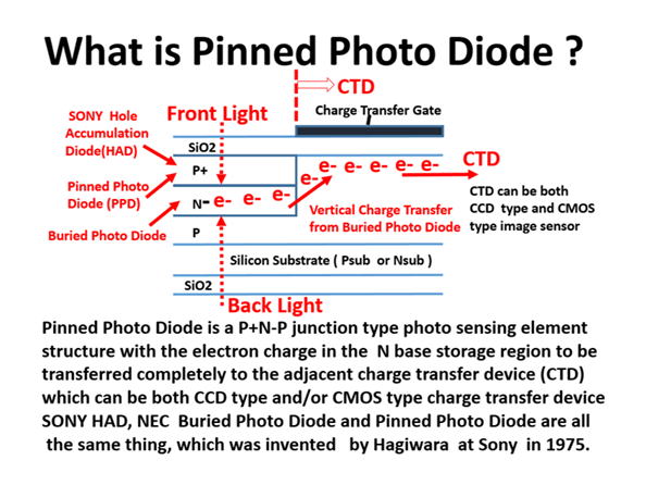
The P+ ( Hole Accumulatio ) top layer has
the stable fixed ( Pinned ) voltage, quenching
Silicon-SiO2 interface trappig noise and the
surface-recombination-center induced dark
current.
These device physics effects are explained
in details in the Hagiwara 1975 PhD thesis
which was written by Hagiwara as a CalTech
graduate student with the guidance of Prof.
C.A.Mead, Prof.T.C.McGill and Prof.James
McCaldin in Gordon Moore Lab at CalTech,
Pasadena California, USA in 1972 to 1975.
******************
See the two basic Japanese patents Hagiwara
filed at SONY ( JA 1975-127647 ) for the
NPNN+ junction type Pinned Photo Diode with
thinned silicon BACK LIGHT illumination and
( JA-134985 ) for the P+N-PNsub junction
(thyristor) type Pinned Photo Diode with
the vertical overflow drain (VOD) function mode
as shown below.
******************
How could Fossumu be the developper of
the modern CMOS digital image sensor ?
******************
Based on the dilligent works of SONY
people, Hagiwara now is going to explain
why Hagiwara believes that Fossum and
Teranishi-san are the WRONG and FAKE
PEOPLE . They are liars and crooks. They
are politically-working dishonest people
now governing the image sensor comunity.
Fossum did not know the basic patent
on the Back Light illuminated Pinned
Photo Diode ( JA 1975-127647 ) which
is the basic light detection structure of
the modern CMOS digital image sensor
with Back Light Illumination. Hagiwara
at SONY invented this structure at SONY.
Fossum did not develop any built-in A/D
converters which is needed INSIDE of the
CMOS digital image sensor chips. Asano,
Yamada and Fukushima did the pioneering
works in SONY. Their dilligent works at
SONY made SONY possible to introduce
the compact CMOS digital image sensor on
the market for the first time in the world.
The Snap Shot digital circuits needed in
CMOS image sensors was developped by
Pain and his coworkers in JPL ,CalTech.
Active circuits in CMOS image sensors
were developpped by Phyllips people.
Fossum did not develop any Fast Cache
SRAM needed for digital camera systems
for quick digital image data aquisition.
The pioneering Fast Cache SRAM works for
the real time digital TV broadcast systems
were developed by Miyaji and Hagiwara in
SONY in 1989 . Later this technique helped
to realize the SONY compact digital camera.
Fossum did not do anything to develop any
nonvolatile memory chip, NVRAM chips with
the floating gate MOS memory device, which
was invented by Prof. S. Sze and his coworker
in Bell Lab and later developped in the form
of the NAND Flash memory at Toshiba by
Prof. Tonooka in Tohoku University.
With all of these technologies, SONY young
engineers developped for the first time in
the world the thinned wafer BACK LIGHT
illumination CMOS digital image sensor with
the SONY original HAD sensor, which is the
same thing as the one the world is calling
commonly as the Pinned Photo Diode now.
This Pinned Photo Diode with BACK LIGHT
illumination is the very invention of Hagiwara
as shown below.
******************
**********************************************************************
In June 2018, Hagiwara was not very happy
when Hagiwara learned that Teranishi-san ( ex-NEC )
was awarded with Queen Elizabeth Award 2017
as the inventor of Pinned Photo Diode, which was
based on his 1982 IEDM paper on the Buried Photo Diode
in the Interline Transfer CCD image with no image lag.
The decison was obvioously made by the 2014 Fossum Fake Paper
that made also the world to belive that Fossum was the developer
of the Modern CMOS digital camera. The truth is that SONY young
dilligent silent engineers worked hard to realize the Modern Highly
l
Light sensitive and LOW DARK CURRENT CMOS digital Camera
with BACK LIGHT illumination.... NOT FOSSUM ... NOT Teranish ....
Hagiwara is not very happy.
The world has the right to know what is the truth.
******************************************************************
http://qeprize.org/winner-2017/
https://en.wikipedia.org/wiki/Queen_Elizabeth_Prize_for_Engineering
******************************************************************
On 1 February 2017, it was announced that the 2017 prize would be awarded
to the four engineers responsible for the creation of digital imaging sensors.
The announcement was made by Lord Browne of Madingley at the Royal Academy
of Engineering, in the presence of HRH The Princess Royal.
The winners of the 2017 prize were:
(1) George E. Smith of United States for the invention of the charge-coupled
device (CCD) principle
(2) Michael Tompsett of UK for the development of the CCD image sensor,
including the invention of the imaging semi-conductor circuit and the analogue-to-digital converter
(3) Nobukazu Teranishi of Japan for the invention of the pinned photodiode
(PPD)
(4) Eric Fossum of United States for developing the CMOS image sensor
Together, their innovations allowed for advancements in medical treatments,
science,
personal communications and entertainment.
The winners will receive their award in a ceremony at Buckingham Palace later in 2017.
******************************************************************************
However, from the evidence shown below, it is clear that Hagiwara is the
true inventor
of Pinned Photo Diode. Hagiwara is not very happy now by the bad news above.
************************************************************
Fossum 2014 Fake Paper
************************************************************
It all started from the Fossum 2014 fake paper on Origin of Pinned Photo Diode.
************************************************************
Prof. Albert Theuwissen said that Fossum 2014 paper is doutful.
Prof. Akira Matsuzawa said that Fossum 2014 paper is fake.
Prof. Shingo Kagami said that SONY HAD ( which was invented by
Hagiwara in 1975 ) and the Pinned Photo Diode are the same thing.
The details of Hagiwara 1975 patents prove that Fossum is a big liar,
telling a big lie on the origin of Pinned Photo Diode.
Fossum said in his 2014 fake paper that Hagiwara 1975 Patent
invention did not describe any charge transfer operations,
which is a very, very big lie , deceiving the entire world,
including Queen Elizabeth of United Kingdom and also
the Emperor of Japan !!!!!!
The following two patents filed by Hagiwara at SONY
in 1975 clears shows that the two Hagiwara Patents
clearly define the Pinned Photo Diode structure with
the complete charge transfer operation mode.
*****************************************************
Fundementals and Brief History of Solid State Image Sensors
*****************************************************
(1) What is CCD ?
A charge-coupled device (CCD) is a device for the movement of electrical charge,
usually from within the device to an area where the charge can be manipulated,
for example conversion into a digital value.
CCD is a simple structure of many MOS type charge transfer electrodes,
next to each other in series, placed on the oxide semiconductor surface.
These MOS type capacitors of CCD are biased above the threshold
for inversion when image acquisition begins, allowing the conversion
of incoming photons into electron charges at the semiconductor-oxide interface
in case of the original surface type CCD invention in 1969.
See https://en.wikipedia.org/wiki/Charge-coupled_device
(2) What are the two important functions of CCD ?
In the CCD image sensor pixels for light detection are represented
by metal-oxide-semiconductors (MOS) capacitors. The CCD is then
also used to read out out these charges as an analog shift register.
CCD moves signal charge between capacitive bins in the device,
with the shift allowing for the transfer of charge between bins.
CCD works as a photo detection structure and also as an analog shift register.
This is achieved by "shifting" the analog signal packets between stages within
the device one at a time. Charge Coupled Device is an analog shift register.
Charge Coupled Device works as an analog signal packet transmission line.
(3) What is wrong with the original surface channel type CCD ?
The original surface channel type CCD had two problems.
One of the two problems is the poor charge transfer efficency of 99.9 %.
However, the original surface channel type CCD invented in 1969 have only 99.9 %
of charge transfer efficiency. It means that, after less than 1000 times of charge
transfer shift-operations, the original analog signal charge is degraded completely.
There the surface type CCD had no practical value. Intel and other companys
gave up of using CCD as digital memory device due to this poor charge transfer
efficiency and also due to the large power needed to clock the large MOS capacitors
of the charge transfering metal gates of the CCD analog shift register.
The other one of the two problems is the poor blue light sensitivity.
Beside the poor charge transfer efficiency of 99.9 %, because CCD is made of a series
of dynamic charge tansfer MOS gates. The metal electrode does not pass the light
efficently. The meal reflects light like a mirror.
Inherently CCD is not really a good light sensitive detector. CCD has a very poor light
detection capability, specially in the blue and ultra violet lights of short wave length.
Hagiwara working at SONY in 1975 had many video camera engineers. They did not
like CCD video cameras because of the poor color reproduction problem. They liked
the classical MOS image sensor camera of the N+P type photo diode instead of the
CCD type MOS capacitor photo detecting structure. Hitachi and other companys
did not like CCD image sensor cameras and they were focused on developping
the classical video camera of N+P type photo diode type light detecting structure.
(4) What is the buried channel type CCD ?
However, the buried channel type CCD invented in 1971 have 99.999% of
charge transfer efficiency. It means that, even after 1000 times of charge
transfer shift-operations, the 99% of the original analog signal charge is
saved. This analog buried channel type CCD shift register of 99.999% charge
trasfer efficincy worked fairly well for the past NTSC TV picture applications
in the past century.
See https://patents.google.com/patent/US3792322A/en
See https://patentimages.storage.googleapis.com/90/6e/28/e1f0a9b89d5110/US3792322.pdf
(5) What is wrong with the buried channel CCD ?
The buried channel CCD was working well for the NTSC TV picture resolution
cameras in the past. But now the high resolution digital TV era came and we
have now 4K and more high resolution pictures. If we use this CCD analog shift
register of only 99.999% charge transfer, since we need to transfer charge packets
more than 7000 charge transfer operations, that is, since "4000H + 3000V" means
7000 charge transfers, we lose now 7 % of the original signal charge at the end of
the 7000 bit CCD analog shift register of only 99.999% charge transfer efficiency.
And the reproduced image quality would be very poor.
Besides, the large power needed to clock the large MOS capacitors of the charge
transfering metal gates of the CCD analog shift register is no longer welcomed.
So CCD was a short-lived and we don't need this technology any longer.
The scaling of CMOS process technology tend encouraged and helped very much
the many delligent digital circuit engineers of CMOS image sensor applications.
The total CMOS digital circuit technology now, including the light-detecting Pinned
Photo Diode ( invented by Hagiwara at SONY) , one charge transfer gate of conventional
MOS switching electrode, fast A/D converter digital circuit technology ( developped by
Yamada and Asano at SONY ) , digital data transmission line , fast Cache SRAM of dynamic
floating read-out bit line technolgy ( invented Miyaji and Hagiwara at SONY ) and slow
NVRAM of the floating gate technolgy ( invented by Prof.S.Sze ) all together as a big digital
circuit system technology, finally replaced the Giant Super Star the CCD, the analog shift
register techology.
Beside the poor charge transfer efficiency of 99.9 %, because CCD is made of a series
of dynamic charge tansfer MOS gates. The metal electrode does not pass the light
efficently. The meal reflects light like a mirror.
Inherently CCD is not really a good light sensitive detector. CCD has a very poor light
detection capability, specially in the blue and ultra violet lights of short wave length.
(6) What replaced the CCD-type MOS capacitance photo detecting structure ?
In 1975 Hagiwara replaced the CCD-type MOS capacitance photo detecting structure
with the light detecting structure of the P+N-PNsub junction ( PNP transitor in
N-type substrate ) type , which is now called a Pinned Photo Diode.
He filed two Japanese patents, one for the P+N-PNsub junction type Pinned
Photo Diode with the vertical overflow drain (VOD) function ( JA 1975-134985 )
and the other one for the NPNN+ junction type Pinned Photo Diode with the
thinned silicon die with back light illuminati ( JA 1975-127647 ) which is now
the basic light detection structure of the modern digital CMOS image sensor.
Hagiwara studied the buried channel CCD in his PhD work in CalTech. Hagiwara
understood both the strong and the weak points of the buried channel CCD.
Hagiwara gave up of using CCD as the light detecting structure. Instead Hagiwara
focused to use the N+P photo diode for the light detecting structure.
Hagiwara was trained in SONY bipolar fabrication lines at Sony Atsugi Technoogy
Center in Japan in 1971 and 1972. And Hagiwara understood very well the P+NP
transisitor structures and reliability problems such as the P+NPNsub thyristor
puch-thru operation mode of the P+NP transitor formed in the N-type substrate
Nsub die.
He filed two Japanese patents, one for the P+N-PNsub junction type Pinned
Photo Diode with the vertical overflow drain (VOD) function ( JA 1975-134985 )
and the other one for the NPNN+ junction type Pinned Photo Diode with the
thinned silicon die with back light illuminati ( JA 1975-127647 ) which is now
the basic light detection structure of the modern digital CMOS image sensor.
The CCD-type MOS capacitance photo detecting structure is now replaced by
the Pinned Photo Diode invented by Yoshiaki Hagiwara at Sony in 1975.
The world did not know the truth.
The truth is that, CCD is not a very good light detecting structure,
The MOS-capacitance type CCD light detector has a very poor light
seisitivity and also has very bad trap noise and dark current at the
Oxide-Semiconductore inteface.
On the other hand, the P+NPNsub junction ( thyristor ) type light
detecting structure ( JA 1975-134985 ) invented by Hagiwara in SONY
in 1975 is a very good light detecting structure with very low trap noise
and dark current because the the Oxide-Semiconductore inteface states
are all quenched by the Hole Accumuation P+ region which is pinned at
stable voltage value. This is the reason why SONY called it as the SONY
original HAD sensor, and why the world called it as the Pinned Photo Diode.
The Pinned Photo Diode, invented by Hagiwara in 1975, replaced the
CCD-type MOS capacitance photo detecting structure. SONY annouced
in Tokyo by SONY President Kazuo Iwama and at the same time in New
York by SONY Chairman Akio Kazuo to the public widely in the world
SONY new video camera with excellent light detection capability and
with the very low trap and dark current features of high quality pictures.
These good features were owing to the Hagigiwara's new invention on
the P+NPNsub junction photo diode ( now called Pinned Photo Diode),
but the world misunderstood that CCD image sensor was so. But the
truth is that, CCD image senor was not. Hagiwara Photo Diode was !
In 1975 Hagiwara replaced the CCD-type MOS capacitance photo detecting
structure with the new light detecting structure of the P+N-PNsub junction
( PNP transistor structure in N-type substrate ) type light detecting photo
diode structure , which is now called a Pinned Photo Diode
So, the orignal CCD was expected to perform two important functins of
the light detction and the analog data transmission line.
In recent years CCD has become a major technology for digital imaging.
But the truth is that, CCD was saved by Hagiwara 1975 invention introduing
to the world a new light detecting photo diode structure in the SONY 1978
Press Conference in Tokyo and New York.
Although CCDs are not the only technology to allow for light detection,
CCD image sensors are widely used in professional, medical, and
scientific applications where high-quality image data are required
because the Hagiwara 1975 invention of the Pinned Photo Diode was
always in the behind back curtain helping CCD image sensors.
But the world did not know that CCD works only as an anlalog data
transimission line. The light detecting photo diode structure invented
by Hagiwara in 1975 gives the features of professional, medical, and
scientific applications where high-quality image data are required.
In applications with less exacting quality demands,
such as consumer and professional digital cameras,
the light detecting photo diode structure invented
by Hagiwara in 1975 was also used as active pixel sensors.
The world thought CCD is the one giving all the imortant
features of of professional, medical, and scientific applications
where high-quality image data. But the true hero was behind
the curtain. CCD was on the stage. Hagwara 1975 invention
helped CCD on the stage. Now CMOS digital circuit technology
took over the CCD analog technology, and CMOS image sensor
is now on the world stage. But still Hagiwara 1975 invention
behind the back curtain was helping CMOS digital image
sensor on stage. Hagiwara 1975 invention was alwasys helping
image sensors on the high lighted stage in the world.
Now Hagiwara, at age 70, should be happier if the world knew that
the Pinned Photo Diode was acturally invented by Hagiwara in 1975
when Hagiwara was just 26 years old, a young dreaming SONY engineer.
************************************
Hagiwara invented Pinned Photo Diode in 1975
Hagiwara developped Digiltal CCD and CMOS Image Sensors
Hagiwara Patent Pictures on Pinned Photo Diode
https://patents.justia.com/inventor/yoshiaki-hagiwara
************************************
Queen Elizabeth of the United Kingdom
and the Emperor of Japan Gave Awards
to WRONG and FAKE PEOPLE ??.
*************************************************************************************
In June 2018, Hagiwara was not very happy
when Hagiwara learned that Teranishi-san ( ex-NEC )
was awarded with Queen Elizabeth Award 2017
as the inventor of Pinned Photo Diode, which was
based on his 1982 IEDM paper on the Buried Photo Diode
in the Interline Transfer CCD image with no image lag.
The decison was obvioously made by the 2014 Fossum Fake Paper
that made also the world to belive that Fossum was the developer
of the Modern CMOS digital camera. The truth is that SONY young
dilligent silent engineers worked hard to realize the Modern Highly
l
Light sensitive and LOW DARK CURRENT CMOS digital Camera
with BACK LIGHT illumination.... NOT FOSSUM ... NOT Teranish ....
Hagiwara is not very happy.
The world has the right to know what is the truth.
*************************************************************************************
http://qeprize.org/winner-2017/
https://en.wikipedia.org/wiki/Queen_Elizabeth_Prize_for_Engineering
*************************************************************************************
On 1 February 2017, it was announced that the 2017 prize would be awarded
to the four engineers responsible for the creation of digital imaging sensors.
The announcement was made by Lord Browne of Madingley at the Royal Academy
of Engineering, in the presence of HRH The Princess Royal.
The winners of the 2017 prize were:
(1) George E. Smith of United States for the invention of the charge-coupled
device (CCD) principle
(2) Michael Tompsett of UK for the development of the CCD image sensor,
including the invention of the imaging semi-conductor circuit and the analogue-to-digital converter
(3) Nobukazu Teranishi of Japan for the invention of the pinned photodiode
(PPD)
(4) Eric Fossum of United States for developing the CMOS image sensor
Together, their innovations allowed for advancements in medical treatments,
science,
personal communications and entertainment.
The winners will receive their award in a ceremony at Buckingham Palace later in 2017.
**************************************************************************************************
However, from the evidence shown below, it is clear that Hagiwara is the
true inventor
of Pinned Photo Diode. Hagiwara is not very happy now by the bad news above.
In the most simplest form of a Pinned Photo Diode is P+NP junction ( transistor ) type
photo diode with the emitter P+ region and the collector P region is connected (pinned)
to a stable fixed ( pinned ) voltage.
The base N region is shallowly doped, which is enabling the complete majority-carriers
charge-transfer, resulting an empty potential well of the completely majority-carrier
depletion mode in the base N storage region.
The signal majority carriers are completely transferred to an adjacent Charge Transfer
Device (CTD) which can be a classical simple NMOS type, a FT CCD type, an ILT CCD
type and the modern CMOS type active Charge Transfer Devices (CTDs).
In 1978, SONY announced a CCD image sensor video camera with this highly light sensitive
and very low dark current P+NP junction type Pinned Photo Diode in Tokyo by SONY
President Kazuo Iwama and in New York by Sony Chairman Akio Morita at the same time.
The world misunderstood that the CCD image sensor is highly light sensitive and of very
low dark current. But the truth is, the P+NP type Pinned Photo Diode sensor which was
invented by Hagiwara in 1975 was highly light sensitive and of very Low dark current.
The surface type CCD had only 99.9 Charge Transfer Efficiency and was no use for the
Consumer Video Camera applications. But the buried channel type CCD had 99.999%
Charge Transfer Efficiency which was good enough for NTSC TV picture quality.
But CCD is not enough for the modern High Resolution Digital TV.
CCD is an analog shift register, which is a kind of an analog signal transmission line.
The analog technolgy is all now to be replaced by the new modern digital technology.
We now use a digital shift register with A/D converter CMOS digital circuits,
which is a kind of a digital signal transimission line.
So CCD was a short-lived analog technology. We do not need CCD any more.
Now we have CMOS type Charge Transfer Device which is a digital data transmission line.
All of this became possible owing to the advance of scaling down of CMOS fabrication
technology which minituarized the CMOS gate electrode size, the wiring meal line
dimensions, the metal contact size and the size of diffusion area and depth. All of them
now contibute for minimizing the CkT noise and Clock noise in CMOS image sensors.
We now have (1) Pinned Photo Diode (2) One Charge Transfer Gate (CTD) (3) A/D converter
(4) Digital Signal Transmission Line ( just digital circuits ) (5) Fast Cache SRAM for qick
digital picture data aquision, and finally (6) Nonvolatile Memory (NVRAM) in the modern
small conpact CMOS digital image sensor camera.
Compact and Handy Consumer Digital Camera must be by definition small and compact.
SONY enginners worked very hard to realize SONY original HAD CCD and CMOS degital
cameras. Howerver, outside SONY, the SONY brand name, SONY original HAD, is not used.
Instead, it is called worldwide the Pinned Photo Sensor. The truth is, the Pinned Photo
Diode and SONY original HAD sensor are the same thing that Hagiwara invented in 1975.


*******************************************************************
See also three invited talks related to SONY HAD sensor now called also
as Pinned Photo Diode.
(1) International Conference CCD79 in Edinburgh, Scotland UK
(2) International Conference ESSCIRC2001 in Vilach, Austria.
(3) International Conference ESSCIRC2008 in Edinburgh, Scotland UK
*******************************************************************
As seen above from the two original Japanese Patents filed by Yoshiaki
Hagiwara at SONY in 1975,
it is very clear that Hagiwara is the true inventor of the Pinned Photo
Diode.
But Hagiwara is not happy now because the world does not understand this
fact.
The details are explained below.
*************************************************************************************
In June 2018, Hagiwara was not very happy
when Hagiwara learned that Teranishi-san ( ex-NEC )
was awarded with Queen Elizabeth Award 2017
as the inventor of Pinned Photo Diode, which was
based on his 1982 IEDM paper on the Buried Photo Diode
in the Interline Transfer CCD image with no image lag.
*************************************************************************************
http://qeprize.org/winner-2017/
https://en.wikipedia.org/wiki/Queen_Elizabeth_Prize_for_Engineering
*************************************************************************************
On 1 February 2017, it was announced that the 2017 prize would be awarded
to the four engineers responsible for the creation of digital imaging sensors.
The announcement was made by Lord Browne of Madingley at the Royal Academy
of Engineering, in the presence of HRH The Princess Royal.
The winners of the 2017 prize were:
(1) George E. Smith of United States for the invention of the charge-coupled
device (CCD) principle
(2) Michael Tompsett of UK for the development of the CCD image sensor,
including the invention of the imaging semi-conductor circuit and the analogue-to-digital converter
(3) Nobukazu Teranishi of Japan for the invention of the pinned photodiode
(PPD)
(4) Eric Fossum of United States for developing the CMOS image sensor
Together, their innovations allowed for advancements in medical treatments,
science,
personal communications and entertainment.
The winners will receive their award in a ceremony at Buckingham Palace later in 2017.
**************************************************************************************************
Before going into the details of the Pinned Photo Diode,
the background information about Hagiwara's early
engineering works are first explained briefly here.
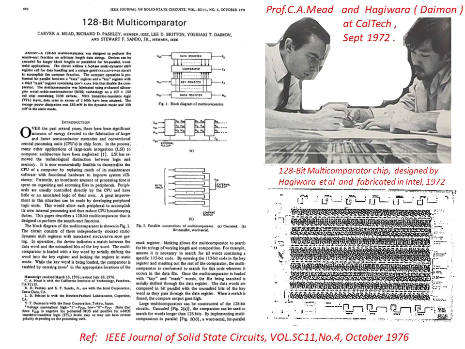
Hagiwara also designed a MOS digital LSI chip,
a 128 bit Multicomarator silicon chip,
when he was a graduate student at CalTech.
Prof. C.A.Mead was one of his PhD thesis advisers.
Prof. C.A.Mead and Dr. Gordon Moore are also CalTech graduates.
They both are good friends, and they met each other frequently
in our reserch lab at CalTech. Our CalTech EE department lab
is now called as Gordon Moore Lab of Electrical Engineerings..
The 128 bit multicomparator chip was designed by Hagiwara
and other fellow students in 1972 with Prof. C. A. Mead's advice,
and was fabricated in the Intel MOS process line with helps of
many CalTech graduates in Intel.
The results were published later in 1976 in IEEE Journal of
Solid State Circuits, VOL.SC-11, No.4, October 1976.
By that time, Hagiwara had graduated from CalTech and was
working in SONY, Japan for making image sensors and video
camera system LSI chip set for consumer digital camera.
Haiwara is the true inventor of the Pinned Photo Diode and
many dilligent SONY engineers and Hagiwara worked together
very hard to build the first CCD digital camera.
And now many dilligent SONY engineers of younger generations
worked togerther to build the first CMOS digital camera with
the backside illumination and in the stacked digital chip formation
which includes A/D Converter , Memory and Processor Units.
CCD and CMOS digital cameras were both developed by SONY.
Hagiwara taught young SONY engineers about digital LSI circuit
design techniques, which Hagiwara himself studied in CalTech
with Intel , HP, IBM engineers. All of them including Hagiwara
were once students of Prof. C.A. Mead in CalTech.
In the PS3 project by SONY, Toshiba and IBM, Hagiwara later
learned that one senior PS3 design engineer Hagiwara worked
together was also a CalTech graduate who used to study and
work in the same Gordon Moore EE Lab in CalTech.
****************************************
Yoshiaki Hagiwara of SONY is the inventor of Pinned Photo Diode.
https://patents.justia.com/inventor/yoshiaki-hagiwara
Pictures of Pinned Photo Diode invented by Hagiwara in Patnet 1975
****************************************
*******************************************************
*******************************************************************
Digital CMOS Image Sensor is watching at its inventor, Yoshiaki Hagiwara.
Hagiwara is the Inventor of SONY HAD and Pinned Photo Diode Image Sensors.
*******************************************************************
**********************************
Please purchase and read
"The world of Digital Circuit Systems
that supports the artificial intelligent
partner systems (AIPS). " written in
Japanese by Yoshiaki Hagiwara in 2016.
ISBN 978-4-88359-339-2 C3055
Price 9000 Japanse Yen and TAX.
B5 size Hard Cover 475 pages
Publisher Seizansha_Inc
Tel +81-42-765-6460
https://www.seizansha.co.jp/ISBN/ISBN978-4-88359-339-2.html
*************************************
return to http://www.aiplab.com
**************************************
Hagiwara and his team worked together to build
a Fast 25 nanosec 4 M bit SRAM chip in 1989
to be used as the fast cache memory
for the digital data from digital cameras.
Fast SRAM is needed to store temporarily the digital image data.
However, NVRAM is a very important media to store the data permanetly.
The polysilicon floatig electorode type NVRAM was invented
by Dr. D. Kahng and Prof. S.M. Sze in 1967
when I was a freshman in Caltech,
just about to learn about Feymann Physics.
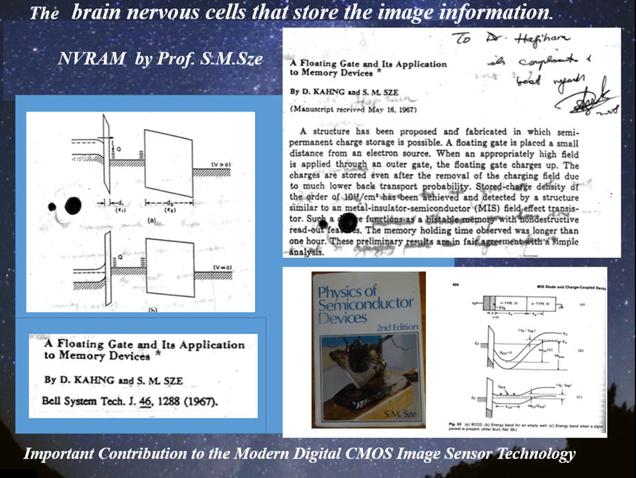
So, in order to build one digital camera,
we need at least the five basic parts,
(1) PPD (2) CTD (3) ADC (4) SRAM (5) NVRAM.
PPD stands for Pinned Photo Diode which is the same thing
as the SONY original HAD ( Hole Accumulation Diode )
which was invented by Yoshiaki Hagiwara at SONY in 1975.
This is a long story about Pinned Photo Diode.
The pinned photo diode can be applied not only for consumer video cameras
but also for artificailly intelligent (AI) robot vision systems for many
apllications.
Hanoi Tower Problem
Coffee Cup Problem
Artificial Intelligent Robot Vision
In 1975 Hagiwara invented the Pinned Photo Diode for future AI Robot Visions.
Hagiwara invented the Pinned Photo Diode in 1975.
SONY introduced in 1978 a very light sensitive video camera system with the Pinned Photo Diode.
SONY introduced to the world the super light sensitive CCD image with the
Hagiwara Photo Diode,
which later SONY called SONY original HAD sensor and the world called the
same thing as
the Pinned Photo Diode. The truth is that Hagiwara is the inventor of the
SONY original HAD
sensor and also the Pinned Photo Diode. Hagiwara saved CCD which everyone
gave up to use
because CCD has very poor light sensitivity. With Hagiwara's invention,
CCD image sensor
became a very light sensitive image sensor. The truth is that CCD is really
light sensitive.
Hagiwara Photo Diode invented by Hagiwara in 1975 is the super light sensitive
photo diode.
The world did not call it Hagiwara Diode. SONY called it SONY original
HAD sensor. The world
outside of SONY all called it Pinned Photo Diode. But both are Hagiwara's
invention. They
are Hagiwara Photo Diode. SONY HAD sensor is in a sense SONY HAgiwara Diode.
Even the backside illuminated modern CMOS image sensor is based on
the Hagiwara 1975 invention ( 1975-127647 ).
Hagiwara is the inventor of .the backside illuminated PPD image sensor.
Hagiwara is also the inventor of the Schottky barrier type PPD image sensor.
Hagiwara is also the inventor of the vertical charge transfor opration,
that is,
with the completely depleted signal charge storage area by the complete
charge transfer mode operation in the vertical direction in the silicon
crystal.
CCD has a very important feature of Complete Charge Transfer operation,
but CCD charge transfer operation is along the surface of the Silicon cystal.
The Photo Diode Hagiwara proposed in his 1975 patents have the vertical
direction charge trasfer operation with Complete Charge Transfer Modes
as seen in the figures given in Hagiwara 1975 patents.
Yoshiaki Hagiwara received BS(1971),MS(1972) and PhD(1975) degrees from
California Institute of Technology ( CalTech ) in Pasadena, California
USA.
His PhD thesis was about the complete charge transfer mechanism of
the buried channel CCD operations by computer simulation analysis.
Hagiwara published his PhD thesis at the international solid state circuits
conference ISSCC1974, and showed that the newly invented buried channel
CCD has very fast and efficient charge transfer capability, achieving the
99.999% charge transfer efficiency, which is a very important feature for
consumer video camera applications.
The original invention of the sureface type CCD had the charge transfer
efficciency of about 99.9 % which is not enough for any practice application.
Intel gave up making CCD type dynamic memory LSI chips. CCD was well
recognize in early 1970s when Hagiwara started working for his PhD thesis.
But by 1975 most of the companies gave up to any CCD in any LSI chip
business applications. Sony was the only company in the world seriously
working hard on CCD for consumer video cameras for home video systems.
Hagiwara joined Sony on February 10, 1975, right after the PhD final oral
presentation, and soon learned that the camera system engineers did not
like poor light sensitive CCD image sensors, because CCD is composed
of a series of charge transfer metal electrodes, which are inherently
Metal-Oxide-Semiconductor ( MOS ) capacitors, and the metal electrons,
as you know all, do not pass light.
The truth is that CCD image sensor has a poor light sensitivity inherently.
Hitachi engineers were working on the classical MOS image sensors which
have SiO2 exposed N+Psub junction type photo diode which had excellent
light sensitivity.
Hagiwara worked in Sony as a university student trainee in SONY bipolar
transistor process lines in the summers of 1971 and 1973, and understood
the device structures and operations of bipolar transistors, including
the
thyristor punch-thru operaion mode which was undesirable for the
proper operations of the bipolar transistor type LSI chips for SONY
color TV sets.
With the two hints, that is, with Hitachi N+P junction photo diode and
with Sony P+NPNsub junction type bipolar transitor technology,
Hagiwara created a new more powerful photo diode structure.
Hagiwara soon filed two patents on the new photo diode structures
for buried channel CCD type charge transfer device (BCCD type CTD),
But Hagiwara inventions were on the photo diode structures which
can be apllied both for CCD type CTD and also for MOS type CTD.
The new photo diode structures were invented and defined in details
in Hagiwara 1975 patents are shown below. This new photo diode
structure is now called as Pinned Photo Diode, which is also very
identical to the Sony origilal Hole Accumulation Diode ( Sony HAD ).
For the original document, visit and search the Japanese Official Patent
Web :
https://www4.j-platpat.inpit.go.jp/eng/tokujitsu/tkbs_en/TKBS_EN_GM101_Top.action
Put the document number ( 1975-134985 ) for Hagiwara 1975 invention on
the P+NPNsub junction ( thyristor ) type Pinned Photo Diode with vertical
OFD.
For the original document, visit and search the Japanese Official Patent
Web :
https://www4.j-platpat.inpit.go.jp/eng/tokujitsu/tkbs_en/TKBS_EN_GM101_Top.action
Put the document number ( 1975-127647 ) for Hagiwara 1975 invention on
the NPNN+ junction ( NPN transistor structure )type Pinned Photo Diode
with vertical charge transfer to the surface type MOS charge transfer gate.
SONY original HAD and Pinned Photo Diode are the same thing,
both invented and defined in the two Japanese Patents
Please visit the oficial Japanese Patent Search Web Site,
https://www4.j-platpat.inpit.go.jp/eng/tokujitsu/tkbs_en/TKBS_EN_GM101_Top.action
to search Hagiwara's original Japanese Patents and put the following two
document numbers,
Document No. ( 1975-134985 ) on the P+NPNsub junction type PPD Patent
Invention and
Document No. ( 1975-127647 ) on the NPNN+ junction type PPD Patent Invention
、
both filed by Yoshiaki Hagiwara in 1975 at Sony.
See the original Pinned Photo Diode Patent 1975
See three invited talks related to SONY HAD sensor now called also as Pinned
Photo Diode.
(1) International Conference CCD79 in Edinburgh, Scotland UK
(2) International Conference ESSCIRC2001 in Vilach, Austria.
(3) International Conference ESSCIRC2008 in Edinburgh, Scotland UK
Fundamentals of Semiconductor Device Physics
****************************************
Now, What is a semiconductor ?
What is a semiconductor material ?
We can sort any materails into one of the four basic kinds.
You know that there are basically four types of bloods.
Like the blood of four kinds ( A,B,AB,O), there are four kinds ( M, O,
S, X ) of materials.
You don't have to know the details inside of these matrials, such as the
atomic structures,
molecular formations, and other special features of these matrials. All
you have to know is
that there are the four kinds of materials in the world.
To understand what is PPD, you still need something about the semiconductor
materials.
Actually there are two type of Semiconductor (S).
They are P type and N type semiconductors.
So actually our world is made of basically five kinds of
materials ( M, O, N, P, X ) , which is more detailed than ( M,O,S,X ).
We now go one by one.
The first one is Metal ( M ).
You know metal can let electric current pass thru.
Now thesecond one is the insulator ( O ) like glass, ruby and diamond crystals.
The insulator dose not let electric current pass thru.
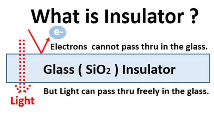
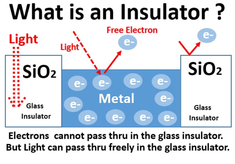
Now the third one is N-type semicnductor (N), whch can let electric current
pass thru and acts like a metal sometimes, but may not let electric current
pass thru at all and acts like an insulator some other times. It is a complex
material. But all you have to know now is that the electric current in
the
N-type semiconductor is produced by moving negatively charged electrons
moving freely in the empty space of the siliocn semiconductor cystal lattice.
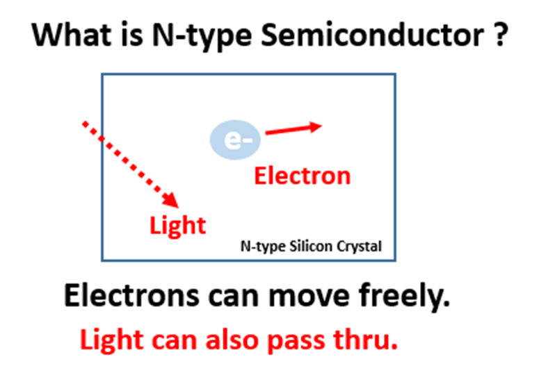
Free electron in the silicon crystal is a negatively charged carrier
which can move freely in the empty space of the N-type semicnductor crystal.
A free electron is like a hard ball in an empty box.
A ball can move freely in the box.
But the ball cannot get out of the box.
A free electons can move inside the silicon crystal .
But the free electron cannot get out of the silicon crystal.
Most of electrons in silicon crystal atoms are bound to the silicon atoms.
Only the electron in the most outer orbit of the silicon atom can move
away
into the empty space in the crystal, if the electron gets enough escape
energy
from illuminated light ( photon enerygy ) or heat ( kinetic enery ).
N-type Silicon Crystal can be manufactured
by adding so-called impurity donor atoms
such as As ( Arsenic ) atoms.
When you prepare a soup, sometimes you add salt and pepper.
The impurity donor atoms are like salt power.
You just add a little bit to the soup.
The soup is like a melted silicon-atom hot liquid.
The melted silicon-atom hot liquid is then cooled very slowly and crystalized
And finally the siliocn liquid becomes a very good slicon crystal .
Those impurity donor atoms capture free electrons in the silicon crystal.
Those impurity donor atoms cannnot move in the Silicon crystal.
Each impurity donor atom, by giving away its most-outer-orbit electron
into the free space in the silicon crystal, becomes an unmovable negatively
charged fixed atom, that is an ionized atom in the silicon crystal.
And now the fourth one, the P-type semiconductor (P).
Now this P-type semicnductor (P), whch can also let electric current
pass thru and acts like a metal sometimes, but may not let electric current
pass thru at all and acts also like an insulator some other times. It is
also a
complex material. But all you have to know now is that the electric current
in the P-type semiconductor is produced by moving positively charged electric
charge carrier, also moving freely in the empty space of the siliocn
semiconductor cystal lattice.
This freely moving positively charged electric charge carrier is called
"hole"
like an empty space ( hole ) in the well-packed box with many balls (electrons).
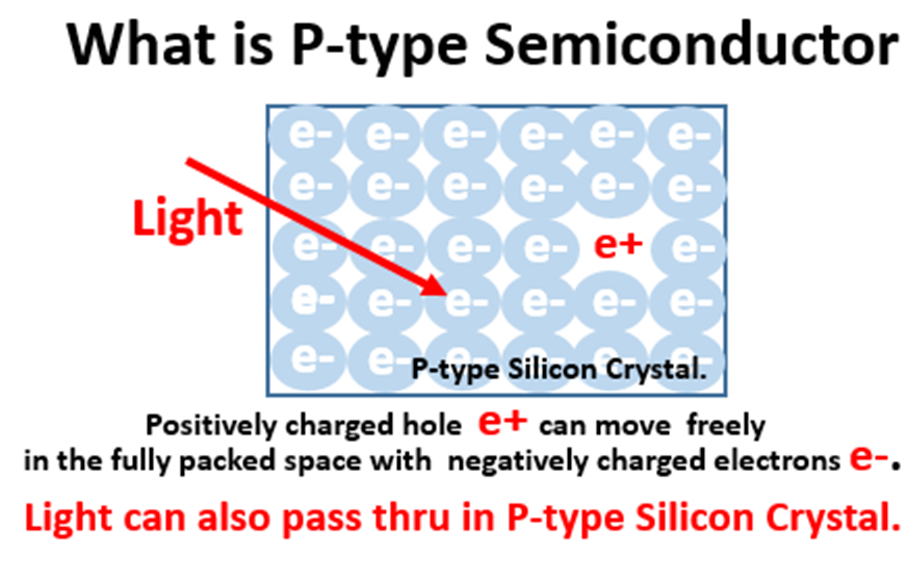
P-type Silicon Crystal can be manufactured
by adding so-called impurity acceptor atoms
such as B ( boron ) atoms.
When you prepare a soup, sometimes you add salt and pepper.
The impurity atoms are like pepper power.
You just add a little bit to the soup.
The soup is like a melted silicon-atom hot liquid.
The melted silicon-atom hot liquid is cooled very slowly and crystalized
And the siliocn liquid becomes a very good slicon crystal .
Those impurity acceptor atoms capture free electrons in the silicon crystal.
Those impurity acceptor atoms cannnot move in the silicon crystal.
Each impurity acceptor atom by accepting an electron becomes
an unmovable negatively charged fixed charge in the silicon crystal.
In P-type silicon, we have no free electrons.
Free electrons are all captured by the acceptor atoms.
These acceptor atoms become negatively charged unmovable atoms.
But the crystal must be kept nuetral.
So there must be a positively charged "something" in the space
surrouding these negatively charged unmovable acceptor atoms.
This positively charged "something" is called a "hole"...
Then, what is a "hole" ?
In P-type silicon crystals, the acceptor atoms such as As (Arsenic) atoms
stole the most oute-orbit electrons in the neighboring silicon atoms.
The charge carrier, which we call "hole" and, can freely move
in the P-type semicnductor is actually a psotively charged
ionized silicon crystal atom whch was deprived of its most-outer-orbit
electron by the neighboring accepter impurity atom.
An impurity atom is a thief.
But, the silicon atom itself cannot move.
Then what is the charge carrier named "hole" ?
I said that most of electrons in a silicon semiconductor crystal are
bound to the atoms in the solid Silicon crystal body.
.
Only the electron in the most outer orbit of the silicon atom can move away
to the empty space in the crystal, if the electron get enough escape energy
from illuminated light ( photon enerygy ) or heat ( kinetic enery ).
But those free electrons are all captured by the unmovable acceptor atoms.
If the most-outer-orbit electron escaped from one silicon atom,
one free electron is generated but it is soon captured by an acceptor
impurity atom in the silicon crystal.
But when the most-outer-orbit electron escaped from one silicon atom,
the originally nuetral silion atom now becomes a positively charged
silicon ion, which has a positive charge.
Effectively an acceptor atom stole one electron from a silicon atom.
The acceptor atom was a thief.
Now the postitively charged siliocn atoms become a thief.
The positively charged silicon can also steal a most-outer-orbit electron
of a neighbouring nuetral silicon atom.
And in return the second atom deprived of the most-outer-orbit electron
now becomes a positively charge hole.
Then this time again, the second siliocn atom becomes a thief,
and will steal an electron from a neighboring silicon atom.
In effect, the positively charge ionized "atomic state" was moved
or junmped from one silicon atom to anaother silicon atom.
Efectively, this positively charged ionaized "atomic state"
behaves like a positive charge carrier and we call it hole (e+) .
Now you know four types ( M, O, N, P ) of the five materils in the world.
Type X is the any material which is an insulator with a black body which
does not pass light and electric current ( elecron flow ).
A house is made of many things, but those things can also classidied
into the five types of matrials ( M, O, N,P, X ).
The pinned photo diode can also built with this basis five types.
In the structrue shown below, we used only four types ( M, O, N, P ).
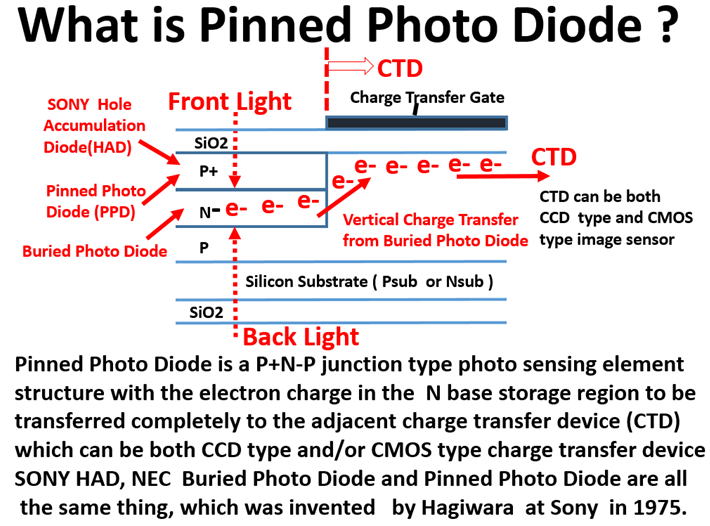
The basic material blocks building PPD are just the four types ( M,O,P,N
)
of basic matrials as you can see in the above figure.
So you now know how the PPD is structured with these basic material blocks.
Now you still do not know how this PPD structure works.
but you now understand the complex structure of PPD which is shown above.
Now we study more in details about the fundemental of
semiconductor device physics and its operations.
Now we study a diode...
Now what is a NP junction diode ?
So we now have P-type and N-type semiconductor materials.
If we connect the two kinds together,
we get a NP junction or PN junction,
which we also call NP diode or PN diode.
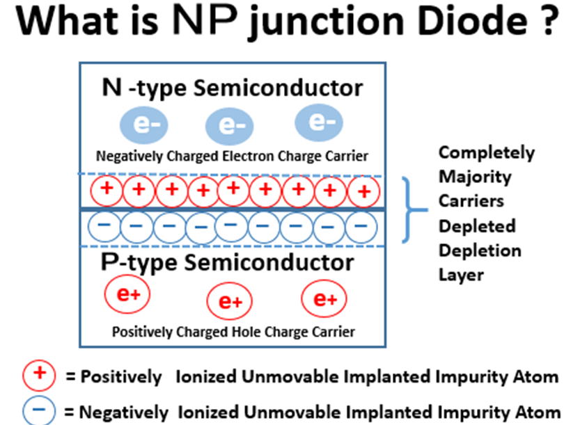
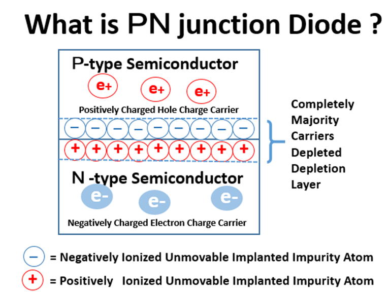
The PN junction is more commonly called so. Why ?
As you see below, if you illuminate light to the PN junction,
you can get electric current to light the house electric bulb.
The electric current flows from the P-silicon terminal to
the N-type silicon turminal. Yes, this PN junction behaves
like a solar cell.
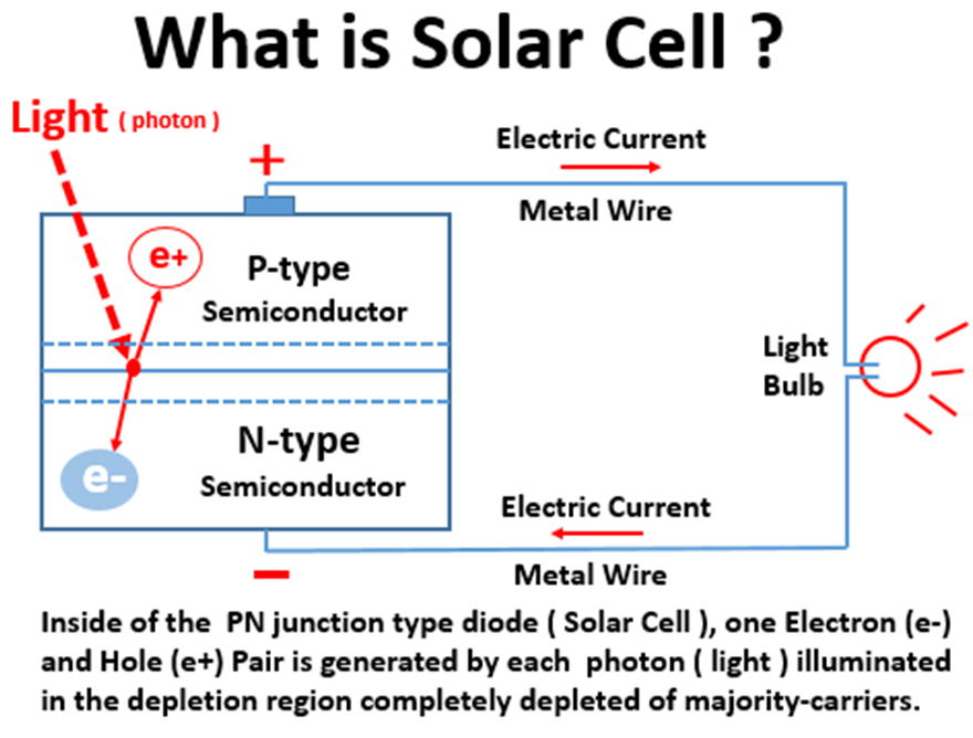
Now if you place these solar cells in the flat large playground, horizontally
4000 cells
and vertically 3000 cells, you can get 12 million pixcel high resolution
image sensor !
Of course, you have to find a way to get each electric current ( electical
signal
charge information ) generated in each solar cell to be transfered to the high
resolution 12 million pixell HOUSE DIGITAL TV .
So we need both highly light sensitive photo diode and charge transfer
device(CTD).
An image sensor needs at least (1) photo diodes (2)Charge Transfer Device(CTD).
Now you understand why the pinned photo diode is so useful.
A pinned photo diode is a very, very small solar cell,
which trasforms many packets of light enerygy ( photons )
into negatively charged elementary partical ( electrons )
which generates electronic energy ( electric current ).
A classical CCD imager was made of (1) Pinned Photo Diode and (2) CCD type
CTD.
SONY introduced the name SONY original HAD which is actually Pinned Photo
Diode.
SONY original HAD ( Hole Accumulation Diode ) and Pinned Photo Diode are
the
same thing, but people in different world business sectors called the same
thing
thing in different ways for the business purpose. It was really confusing,
and still is.
Now, to make a MODEN degital CMOS image sensor, we need (1) Pinned Photo
Diode
(2) CMOS type CTD (3) A/D converter (4) Fast Digital SRAM memory and (5)
Slow
but permanet Nonvolatile memory like a USB memory. We now longer need CCD
type
CTD ( CCD image sensor ) because CCD needs a lot of electric power to clock
the
CCD metal electrode gata, which has a very large electrode gate MOS capacitance.
But the pinned photo diode which was invented by Hagiwara at SONY in 1975
is
still working well in the MODEN degital CMOS image sensors. This 1975 Hagiwara
patents protected SONY image sensors since 1975 to the present for more
than
40 years. There were many patent wars on invention of pinned photo diode.
For the original document, visit and search the Japanese Official Patent
Web :
https://www4.j-platpat.inpit.go.jp/eng/tokujitsu/tkbs_en/TKBS_EN_GM101_Top.action
Put the document number ( 1975-127647 ) for Hagiwara 1975 invention on
the NPNN+ junction type Pinned Photo Diode with vertical charge transfer.
With this simple introduction to the fundamentals of semiconductor device
phyusics,
we are now going to study what is the pinned photo diode in details and
will find out
who is the true inventor of the pinned photo diode, which is also called
as SONY
original HAD. Yes, SONY claimes SONY original HAD is SONY invention, and
if the
pinned photo diode and SONY HAD are the same thing. SONY indirectly is
claiming
that Pinned Photo Diode was SONY invention.
For the original document, visit and search the Japanese Official Patent
Web :
https://www4.j-platpat.inpit.go.jp/eng/tokujitsu/tkbs_en/TKBS_EN_GM101_Top.action
Put the document number ( 1975-134985 ) for Hagiwara 1975 invention on
the P+NPNsub junction ( thyristor ) type Pinned Photo Diode with vertical
OFD.
**********************************************************************************
SONY v.s. NEC and SONY v.s. Fairchild Patent Wars
over Hagiwara 1975 Patents which define
SONY HAD and Pinned Photo Diode image sensors
*********************************************************************************
NEC and Fairchild lost patent wars on this pinned photo diode.
Now both NEC and Fairchild disappered from image sensor business.
Hagiware PPD patents filed in 1975 saved SONY image sensor business.
In 1975, many companies gave up developping CCD image sensor becasse the
CCD image sensor had poor light seisitivity. The reasson is that CCD is
made
of metal electrodes which does not pass light at all. Metal reflects light
like
a mirror. So video camera enginneers did not like the color picture quality
of
CCD imagers. Hitachi engineers were focusing MOS image sensors with
N+P type photo diode. This N+P photo diode had serious image imag lag while
CCD image has no image lag and low clock noise.
Actually, Hagiwara in SONY saved CCD image sensor by intoducing this very
highly sensitive and low noise and imag-lag free photo diode ( PPD or SONY
HAD later called ) in the 1978 Press Conferences in Tokyo and New York.
SONY introduced a highly light sensitive low-noise and image-free CCD video
camera. But the world misunderstood that CCD was highly light sensitive.
The truth is that CCD is highly light sensitive.
The truth is that the Pinned Photo Diode that Hagiwara invented was highly
light sensitive.
In 1975, Hagiwara thought of the lightly doped N-P type photo diode to
reduce
the image lag, making the N-P photo diode to have complete charge transfer
actions to realize image-lag free pictures. He did not file any patent
on this
N-P phioto diode, but he found that P+N-Psub junction type and P+NPNsub
junction type photo diode gives much better stable signal charge and Hagiwara
filed two Japanese basic patents on PPD image sensors.
For the original document, visit and search the Japanese Official Patent
Web :
https://www4.j-platpat.inpit.go.jp/eng/tokujitsu/tkbs_en/TKBS_EN_GM101_Top.action
Put the document number ( 1975-134985 ) for Hagiwara 1975 invention on
the P+NPNsub junction ( thyristor ) type Pinned Photo Diode with vertical
OFD.
In Hagiwara 1975 Japanese Patent on the P+NPNsub junction, the figure shown
below was included, which shows the lightly doped N-P photo diode structure
with the lightly doped N- layer has the same doping level N- of the conventional
buried channel CCD with the lightly doped N- buried channel layer.
For the original document, visit and search the Japanese Official Patent Web :
https://www4.j-platpat.inpit.go.jp/eng/tokujitsu/tkbs_en/TKBS_EN_GM101_Top.action
Put the document number ( 1975-127647 ) for Hagiwara 1975 invention on
the NPNN+ junction ( NPN transistor structure ) type Pinned Photo Diode
with vertical charge transfer to the surface type MOS charge transfer gate.
The official Patent clames on the NPNN+ junction type Pinned Photo Diode
were made in Japanese.
But the official Patent clames were described by one short single paragraph
in Japanese as seen above, with the follwoing important points clearly
explained in Japansee words.
(1) First we must have a die to fabricate any simoconductor device.
The silicon die is called silicon substrate and it can be N type or P
type.
In the example figure shown the substrate was chosen to be N type.
The patent claims and defines only the structure of the photo diode
adjacent to any CTD structure including CCD type and CMOS CTDs.
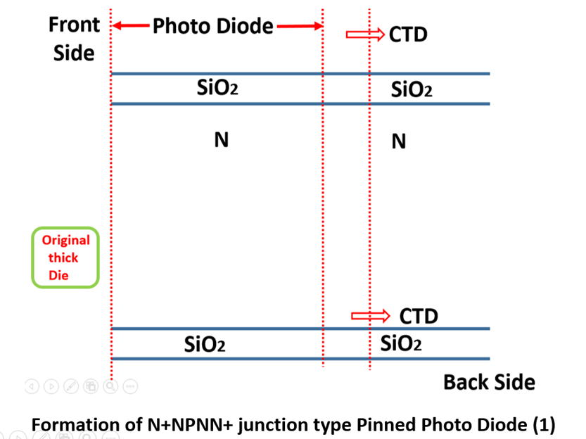
(2) Then MOS metal ( heavily doped polysilicon ) electrodes are formed
to create the charge transfer gate to connet the photo diode structure
to the adjacent charge transfer device (CTD). In the patent example,
the signal charge is positively charged holes (e+) and the charge
transfer gate is a PMOS transistor type.
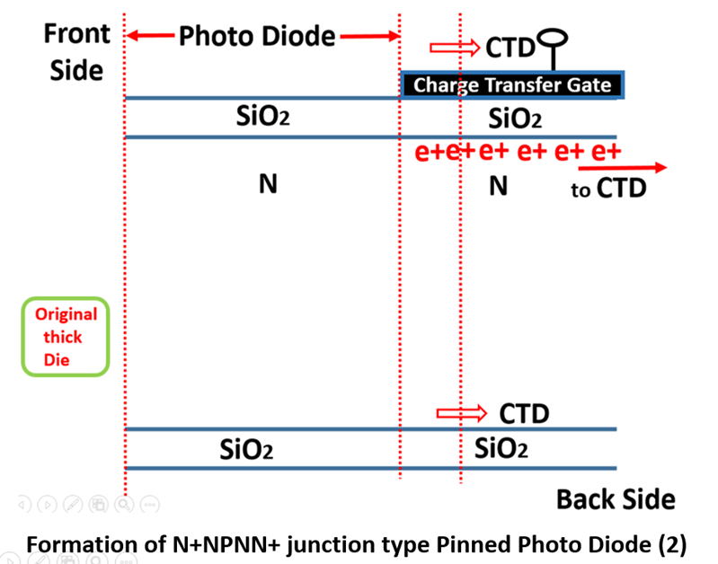
(3) Then the buried P layer is formed ( by deep inplantations) .
This is a very important buried layer signal charge storage layer.
The doping level must be carefully adjusted to the doping level
of the P type buried channel doping level of a conventional
buried channel CCD so that complete charge transfer mode
can be easily achieved in the NPN type junction type PPD.
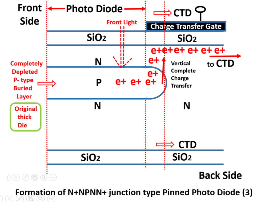
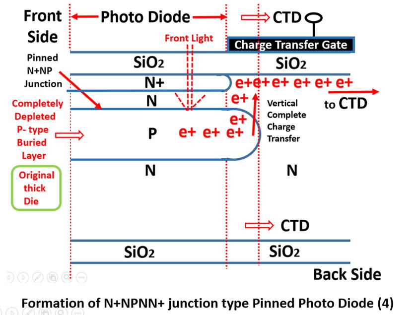
(4) Then, the back side of the die is thinned to make possible also a
Back Light illuminated pinned photo diode image sensor
(5) Then, the back side surface of the silicon substrate is made highly
doped,
to stablize the substrate voltage. By so doing, the NPN diode can operate
as a
upside-down type pinned photo diode with the substrate voltage pinned stably.
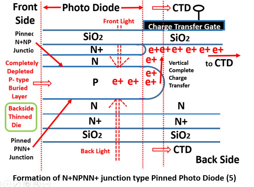
In the patent the charge transfer is a complete depletion mode resulting
the empty
potential well as seen in Figure 7 , implying that it is a completly image-lag
free
operationof picture acqisition. Hence this 1975 Hagiwara invented NPNN+
junction
give a higly light sensitive picture quality with very low surface-generated
dark current.
For the original document, visit and search the Japanese Official Patent
Web :
https://www4.j-platpat.inpit.go.jp/eng/tokujitsu/tkbs_en/TKBS_EN_GM101_Top.action
Put the document number ( 1975-127647 ) for Hagiwara 1975 invention on
the NPNN+ junction ( NPN transistor structure ) type Pinned Photo Diode
with vertical charge transfer to the surface type MOS charge transfer gate.
SONY original HAD super light sensitive digital CMOS .image sensor with back light illumination
is based on this 1975 Hagiwara's invention, which is still working perfectly.
See the very ecellent picture quality of SONY HAD CMOS image sensor (CIS)
below.
SONY held two big press conferences in 1978 on this PNP type pinned photo
diode image sensor.
One is the SONY Tokyo Press Conference 1978 in Tokyo 1978 by SONY president,
kazuo Iwama.
The other one is the SONY New York Press Conference 1978 by SONY chairman,
Akio Morita.
Hagiwara invented the PNP junction type pinned photo didoe, and designed
the PPD FT image
sensor. After careful device/process simulations, Hagiwara himself entered
into the CCD
fabrication line and made the PPD FT image sensor and evaluate the silicon
chip with helps of
some fellow enginners ( Abe, Matsumoto, and Okada ) while most of SONY
engineers were working
on Interline Transfer CCD image sensor, the final goal for SONY video camera
business.
For the original document, visit and search the Japanese Official Patent
Web :
https://www4.j-platpat.inpit.go.jp/eng/tokujitsu/tkbs_en/TKBS_EN_GM101_Top.action
Put the document number ( 1975-134985 ) for Hagiwara 1975 invention on
the P+NPNsub junction ( thyristor ) type Pinned Photo Diode with vertical
OFD.
The charge transfer gate can transfer all the signal charge from the storage area of the PPD sensor
to the adjacent chrage transfer devices ( CTD ). The complete charge transfer mode is possible
which is clearly shown in the figure above in Hagiwara 1975 Japanese Patent
( 1975-134985 ).
The official Patent clames on the P+NPNsub junction type Pinned Photo Diode
are made in Japanese.
But the official Patent clames were described
by one short single paragraph with the follwoing important points
clearly explained in Japansee words.
(1) First we must have a die to fabricate any simoconductor device.
The silicon die is called silicon substrate and it can be N type or P
type.
In the example figure shown the substrate was chosen to be Nsub type.
The patent claims and defines only the structure of the photo diode
adjacent to any CTD structure including CCD type and CMOS CTDs.
In the figure below the transition area between the narrow two hashed
vertical lines is very important part of this patent claim.
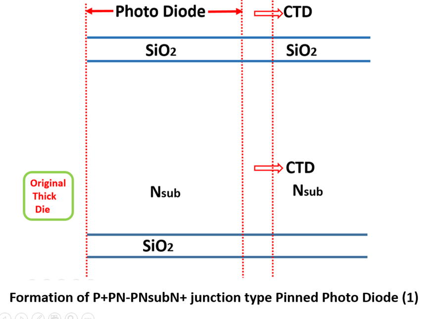
(2) The first step is to form P-type deep well on the N substrate.
If the subsrate is P-type, you do not need this P-type deep well inplantation.
(3) Then the N-type MOS transistor electrodes are to be formed for the
adjacent
charge transfer device (CTD) which can be a CCD type CTD and/or
a CMOS type CTD.
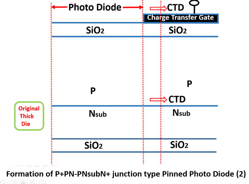
(4) In this case, NMOS type charge transfer gate is formed to transfer
negatively
charged electron signal charge carriers to the adjacent charge transfer
device(CTD).
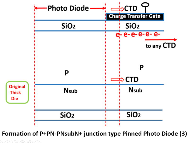
(5) Then a buried N- layer is formed by deep inplantation.
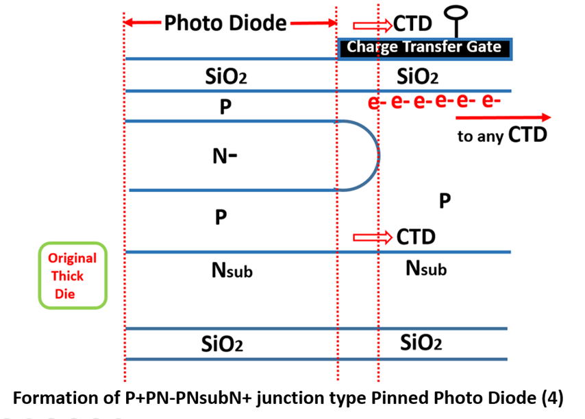
This is a very important buried layer signal charge storage layer
formation to creae the right doping level of the negatively charged
photo elecctron charge carrier storage.
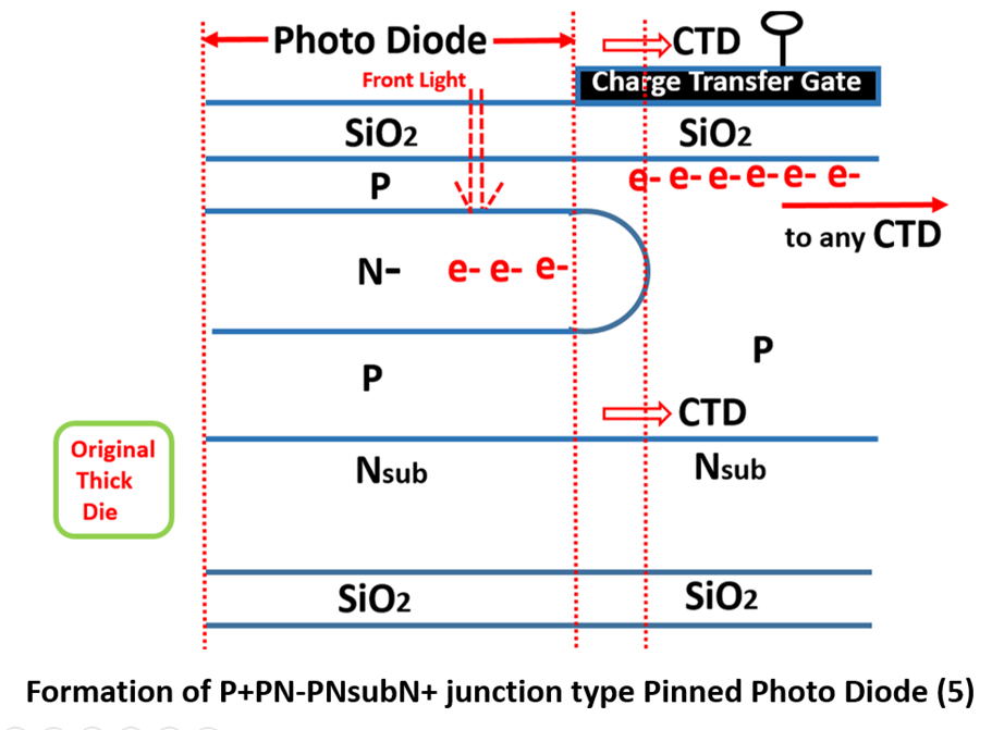
(6) The N- doping level must be carefully adjusted to the doping level
such as the one like the conventional N- type buried channel doping
level of a buried channel CCD so that complete charge transfer mode
can be easily achieved in this PNP type junction type Pinned Photo
Diode ( PPD ) as shown below.
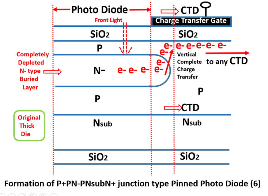
(8) The top P doped space between the SiO2 oxide and theN- buried layer
can be relatively heavily doped P+ region, like the emitter region of
P+NP transistor in order to assure the P+ region is fixed at electrically
stable externally contolable volatge, that is, at a pinned fixed volatge.
This is why this photo diode is called a Pinned Photo Diode.
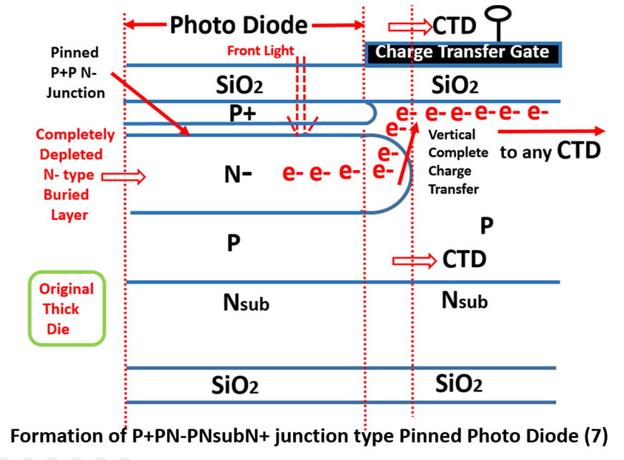
Sony called this Pinned Photo Diode by another name of SONY original
Hole Accumulation Diode simply because this P+ region is concetrated
with accumulated hole majority carriers.
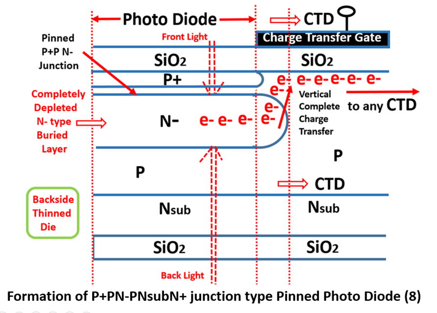
(9) AND finally if the die is thinned, and if the bottom side is doped heavily
to create the heavily doped thin N+ layer as shown below, we can also
have a back light illuminated image sensor.
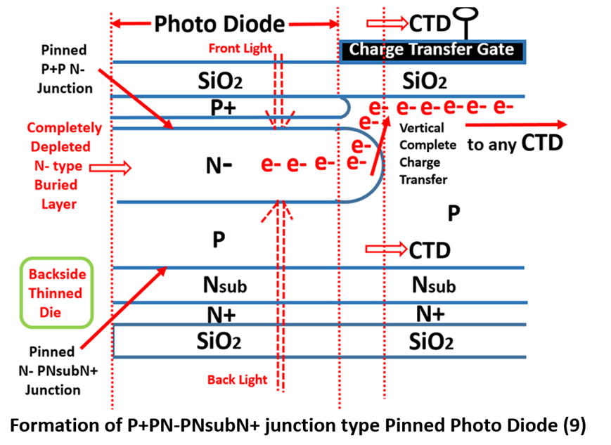
In this way, we finally get the P+NPNsub junction type pinned photo diode
as shown below.
For the original document, visit and search the Japanese Official Patent
Web :
https://www4.j-platpat.inpit.go.jp/eng/tokujitsu/tkbs_en/TKBS_EN_GM101_Top.action
Put the document number ( 1975-134985 ) for Hagiwara 1975 invention on
the P+NPNsub junction ( thyristor ) type Pinned Photo Diode with vertical
OFD.
Hagiwara also invented in 1975 the backside illuminated Pinned Photo Diode
in thinned silicon die
as shown below. This Pinned Photo Diode structure is now being applied in the Modoen Digital
CMOS image sensors with back light illuminated thinned silicon die
For the original document, visit and search the Japanese Official Patent Web :
https://www4.j-platpat.inpit.go.jp/eng/tokujitsu/tkbs_en/TKBS_EN_GM101_Top.action
Put the document number ( 1975-127647 ) for Hagiwara 1975 invention on
the NPNN+ junction ( NPN transistor structure ) type Pinned Photo Diode
with vertical charge transfer to the surface type MOS charge transfer gate.
.
Pinned Photo Diode can be connected to any kind of charge transfer device
(CTD) which includes
CCD type and CMOS type chrage transfer devices, thru the charge transfer gate as shown below.
The charge transfer gate can transfer all the signal charge from the storage area of the PPD sensor
to the adjacent chrage transfer devices ( CTD ). The complete charge transfer mode is possible
which is clearly shown in the figure 7 above in Hagiwara 1975 Japanese
Patent ( 1975-134985 ).
These two original 1975 PPD patents by Hagiwara at SONY shows that
Hagiwara is the true inventor of Pinned Photo Diode(PPD).
*************************************************************************************
In June 2018, Hagiwara was not very happy
when Hagiwara learned that Teranishi-san ( ex-NEC )
was awarded with Queen Elizabeth Award 2017
as the inventor of Pinned Photo Diode, which was
based on his 1982 IEDM paper on the Buried Photo Diode
in the Interline Transfer CCD image with no image lag.
*************************************************************************************
http://qeprize.org/winner-2017/
https://en.wikipedia.org/wiki/Queen_Elizabeth_Prize_for_Engineering
*************************************************************************************
On 1 February 2017, it was announced that the 2017 prize would be awarded
to the four engineers responsible for the creation of digital imaging sensors.
The announcement was made by Lord Browne of Madingley at the Royal Academy
of Engineering, in the presence of HRH The Princess Royal.
The winners of the 2017 prize were:
(1) George E. Smith of United States for the invention of the charge-coupled
device (CCD) principle
(2) Michael Tompsett of UK for the development of the CCD image sensor,
including the invention of the imaging semi-conductor circuit and the analogue-to-digital converter
(3) Nobukazu Teranishi of Japan for the invention of the pinned photodiode
(PPD)
(4) Eric Fossum of United States for developing the CMOS image sensor
Together, their innovations allowed for advancements in medical treatments,
science,
personal communications and entertainment.
The winners will receive their award in a ceremony at Buckingham Palace later in 2017.
**************************************************************************************************
************************************************************
Fossum 2014 Fake Paper
************************************************************
It all started from the Fossum 2014 fake paper on Origin of Pinned Photo Diode.
************************************************************
Prof. Albert Theuwissen said that Fossum 2014 paper is doutful.
Prof. Akira Matsuzawa said that Fossum 2014 paper is fake.
Prof. Shingo Kagami said that SONY HAD ( which was invented by
Hagiwara in 1975 ) and the Pinned Photo Diode are the same thing.
The details of Hagiwara 1975 patents prove that Fossum is a big liar,
telling a big lie on the origin of Pinned Photo Diode.
Fossum said in his 2014 fake paper that Hagiwara 1975 Patent
invention did not describe any charge transfer operations,
which is a very, very big lie , deceiving the entire world,
including Queen Elizabeth of United Kingdom and also
the Emperor of Japan !!!!!!
The following two patents filed by Hagiwara at SONY
in 1975 clears shows that the two Hagiwara Patents
clearly define the Pinned Photo Diode structure with
the complete charge transfer operation mode.
************************************************************
A Prof. Kagami pointed out in his technical presentations, PPD and SONY
original HAD are
the same thing, which was both originally invented by Yoshiaki Hagiwara
at SONY in 1975..
Then SONY original HAD was NEC's invention ???
SONY claims SONY HAD is SONY original.
Something was wrong in this award decision procedures ?
SONY 1978 Press Conference on PDD image sensor was held in Tokyo and New
York.
The following is Hagiwara's claims:
See Japanese Patent JAP 50-134985, invented by Yoshiaki Hagiwara at Sony,
which was filed on Nov 10, 1975 and was publically disclosed as
JAP 52-058414 on May 13, 1977.
Figure 6B shows the completely depleted N charge storage region, which
means
the complete charge transfer operation mode and creates image-lag free pictures
for fast moving action video camera capturings with very fast shutter operations.
For the original document, visit and search the Japanese Official Patent
Web :
https://www4.j-platpat.inpit.go.jp/eng/tokujitsu/tkbs_en/TKBS_EN_GM101_Top.action
So, Pinned Photo Diode is just a PNP junction type photo sensing element semiconductor device,
with the top P region ( Hole Accumulation layer ) pinned to a fixed voltage, protecting the photo
signal electron charge stored in the buried N type storage region underneath from the top
SiO2/Silicon interface charge trapping states. This trap noise was well-known in the surface
type CCD image sensor while the buried channle type CCD image sensor was well-known free
of this charge trap noise. But a strong ellectric field exists at the SiO2/Silicon interface
under the metal electrode of the MOS capacitor structure of the buried channle type CCD
image sensor. Hence, the buried channle type CCD image sensor suffers a large surface
recombination-center generated large dark current.
Also light can easily pass thru the top SiO2 ( tranparent glass ) layor to the PNP junction
while the CCD type photo sensing element structure inherently has the metal electrode
on the top and light cannot pass thru the metal CCD electrode.
Hence the CCD type ( MOS capacitor ) photo sensing element structure has inherently
poor light sensitivity and also, by the surface electric field, the recombination-center
generated large dark current.
In 1975, Hagiwara invented this P+NPNsub junction ( thyrisor ) type Pinned Photo Diode,
and SAVED the CCD image sensor from its extinction.
At that time, many company tried for a long time but gave up CCD image sensor development
efforts due to the poor light sensitivity and the storng surface electric field generated dark
current and the trap noise of the SiO2/Silicon interface state of the CCD MOS capacitor type
photo sensing element sturucture. Intel had given up in developping CCD type dynamic memory
chip and was focused to develop the conventional DRAM in the convention MOS technology.
Hitachi gave up in developping CCD image sensor, and worked on MOS image sensor, expecting
that in the future the MOS transistor scaling rule will reduce the signal
noise (CkT noise) of
the metal wire and difuusion layer capacitance drastically small to the CCD CkT noise level.
Besides, the CCD ( MOS capacitor ) type photo sensing element sturucture dose not have
the vertical overflow drain (VOD) function builti-in and which was also not attractive.
The P+NPNsub junction is a thyristor type photo sensing element structure which can
act as a normal thyristor that is well-known to act in the thyristor punch-thru mode ,
which is exactly the built-in function mode of the vertical overflow drain (VOD) in the
P+NPNsub junction ( thyristor ) type photo diode, which was invented and defined
in the 1975 Hagiwara Japanese Patent ( 1975-134985 ) as shown below.
Hagiwara, with his 1975 invention of this P+NPNsub junction ( thyristor ) type photo
sensing element sturucture SAVED the CCD imager.
SONY enjoyed a big profit, by Haiwara 1975 invention, over the CCD image sensor business
and now in the big CMOS image sensor business.
Fossum 2014 paper shows a figure of Pinned Photo Diode which is quoted below.
You can easily see that the Pinned Photo Diode (PNP junction structure ) shown
in Fossum 2014 paper is completely identical with the PNP junction structure
defined in Hagiwara 1975 Japanese Patent ( JA 1975-134985) shown above.
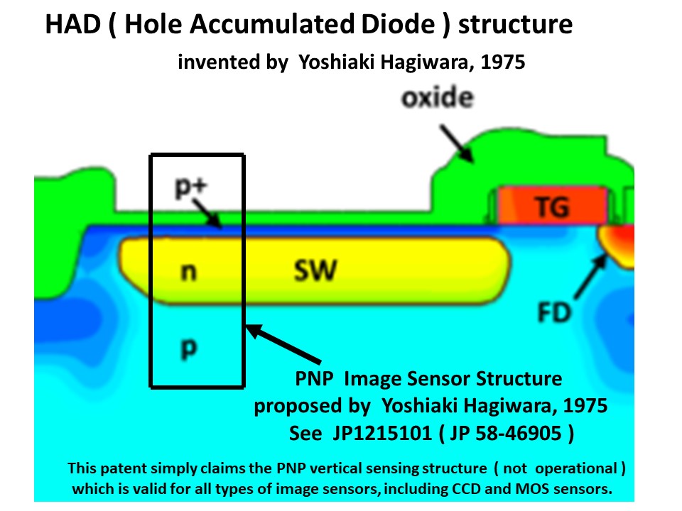
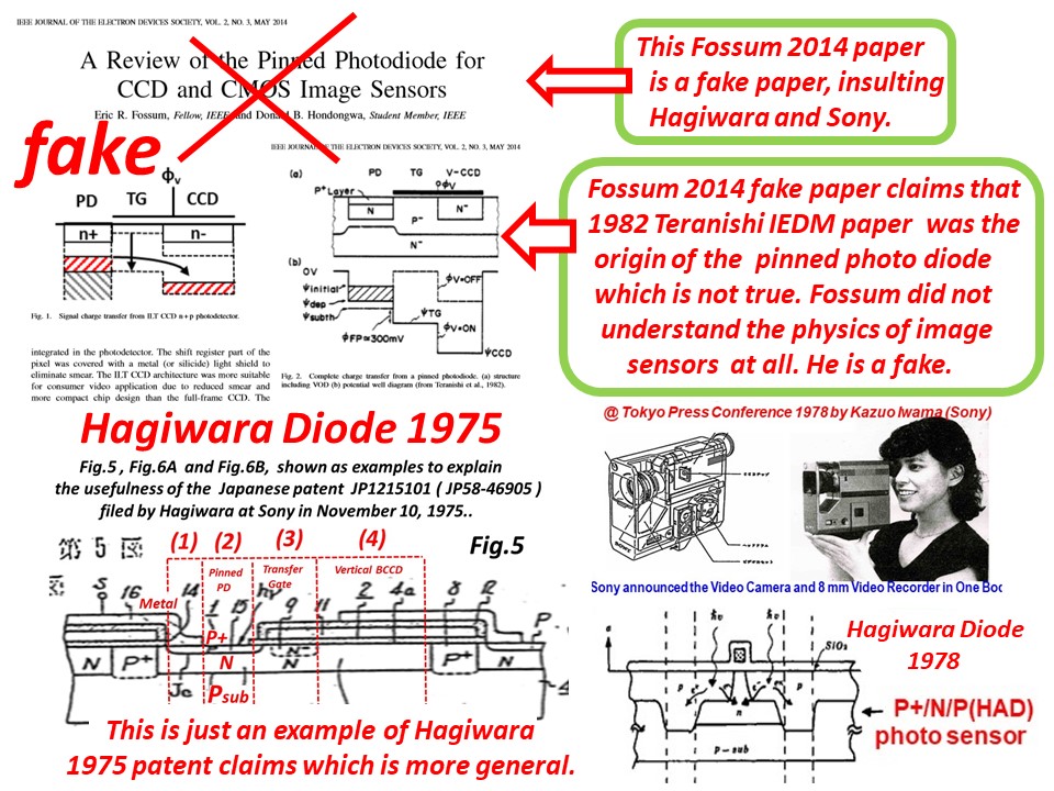
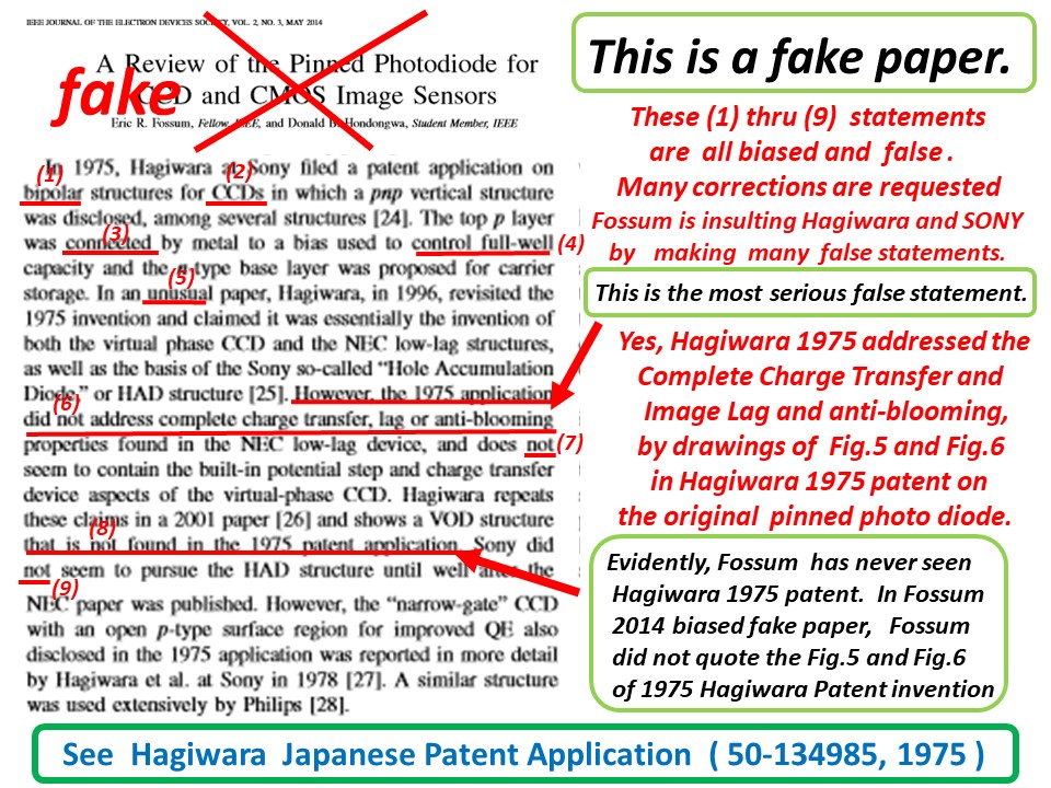
For another Hagiwara 1975 Patent original document,
visit and search again the Japanese Official Patent Web :
https://www4.j-platpat.inpit.go.jp/eng/tokujitsu/tkbs_en/TKBS_EN_GM101_Top.action
Put the document number ( 1975-127647 ) for Hagiwara 1975 invention on
the NPNN+ junction type Pinned Photo Diode with vertical charge transfer,
and back illuminated NPNN+ junction type Pinned Photo Diode on a thinned
die.
This pinned photo diode structure, invented by Hagiwara 1975, is now commonly
applied in Back Light Illunated Modern Digital CMOS Image Sensor in a thinned
silicon die. The figure shown below in Hagiwara 1975 shows clearly the
complete
charge transfer mode operation for image-lag free pictures.
Fossum 2014 paper quotes a figure of Pinned Photo Diode as shown below
with negatively charged electrons as the photo signal charge in the PNP
junction type Pinned Photo Diode.
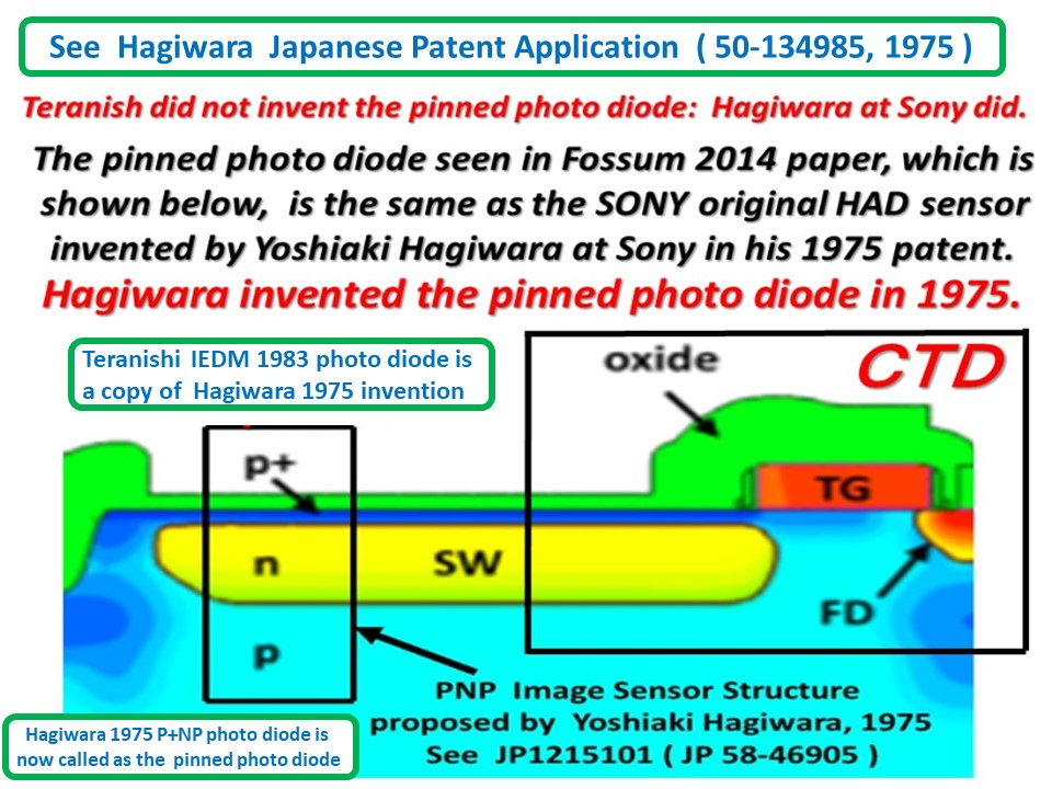
You can easily see that the Pinned Photo Diode ( PNP junction structure ) shown
in Fossum 2014 paper above is completely identical with the NPNN+ junction
type
photo sensing element structure shown below, which was invented by, and
defined
in Hagiwara 1975 Japanese Patent ( JA 1975-127647) shown below.
This time, the NPNN+ pinned photo diode has positively charged holes as
the photo
signal charge, in this case by the N/P symmetry.
The original Pinned Photo Diode (PPD) was invented by Yoshiaki Hagiwara
at Sony
as the P+NPNsub junction ( thyristor ) type photo sensing structure,
which is capable of the vertical over flow drain function
for excess signal charge to be drained out in the vertical direction
that can be easily understood as the various P+NPNsub junction ( thyristor
) action modes.
See also below Japanese Patent JAP 50-127647, invented by Yoshiaki Hagiwara
at Sony,
which was filed on Oct 23, 1975 and was publically disclosed as
JAP 52-051818 on April 26, 1977.
In 1975, Hagiwara also filed a patent on N+NPNsub type Pinned Photo Diode
with vertical
charge transfer function. Light is exposed onto the SiO2 oxide surface
layer, which is
protectiong the top pinned N+N layer of the N+N PNsub junction capacitance type
Pinned Photo Diode.
The figure shown below in Hagiwara 1975 shows clearly the complete
charge transfer mode operation for image-lag free pictures.
As shown in the patent claims of this Japanese Patent ( 1975-127647),
(1) the structure can be fabricated on N-type substrate.
the first region ( N+N layer ) is placed under the SiO2 layer.
(2) And under the first N+N layer is placed the buried second layer ( P
layer ),
which defines the photo singing N+NP junction type Pinned Photo Diode.
(3)This is a patent on a thinned silicon substrate chip.
After the MOS transistor circuits ( including CCD ),
the backside of the silicon chip is to be thinned.
(4) And the backside of the thinned chip is to be heavily doped by N+ atoms,
to quech irregularities of the surface physics, and to form the N+NPN pinned
photo diode.
For the original document, visit and search the Japanese Official Patent Web :
https://www4.j-platpat.inpit.go.jp/eng/tokujitsu/tkbs_en/TKBS_EN_GM101_Top.action
Put the document number ( 1975-127647 ) for Hagiwara 1975 invention on
the NPNN+ junction ( NPN transistor structure ) type Pinned Photo Diode
with vertical charge transfer to the surface type MOS charge transfer gate.
Figure 7 above shows how the PMOS transfer gate is recieving the positive charge ( holes),
the PMOS transfer gate is to be connected to the adjacent charge transfer
devices such as
the interline transfer type CCD and/or the modern CMOS type charge transfer
devices.
So this is the first patent on the backsided iluuminated photo sensor structrure,
the pinned photo diode with vertical charge transfer actions
invented by Yoshiaki Hagiwara at Sony in 1975.
Figure 7 shows how the charge storage region can be depleted completely
of the
signal majority ( carrier positively charge holes ), which means
the complete charge transfer of holes (e+) operation mode.
And this mode of operation also creates image-lag free pictures
for fast moving action video camera capturings with very fast shutter operations.
SONY made the PNP junction type CCD iamge sensor in 1978 and now
the SONY original HAD Modern Digital CMOS Image Sensor (CIS)
with both Front and Back Light illuminated Pinned Photo Diodeas
shown below. SONY Hole Accumulation Diode (HAD) and Pinned
Photo Diode are the same thing, the same structure with two
different names, which is cofusing the world unfortunately....
For the original document, visit and search the Japanese Official Patent
Web :
https://www.j-platpat.inpit.go.jp/web/all/top/BTmTopPage
Put Patent Documentatio Numbers ( 1975-127647 ) and/or ( 1975-134985 )
See the original Pinned Photo Diode Patent 1975
Since this PPD sensor structure has inherently SiO2 exposed photo sensor structure,
very high light sensitivity is expected, specially in the blue short-wavelengh
light.
This PPD sensor can be operated in the complete depletion mode charge transfer
mode
like the conventional buried channel CCD imaging structure.
However the conventional buried channel CCD imaging structure is made of
the metal
oxide capacitance structure and the metal electronde reflects light and
has very poor
light absorption capability, resulting in the very poor light sensitivity specially
in the blue short-wavelengh light is expected.
For solid state image sensors, the sensitivity is the most important feature.
The P+NPNsub junction ( thyristor ) type photo sensing structure,
invented by Yoshiaki Hagiwara at SONY in 1975 can provide
(1) very excellent light sensitivity specially in the blue short-wave light.
(2) the top P+ pinned at a fixed voltage region quenches the surface
dark curret and also the surface trap noise.
(3) The N-type storage charge can be completely depleted of the majority
carrier electrons and transfered to the adjacent charge tarnsfer deive(CTD).
This complete charge transfer operation in complete depletion mode was
well known as the most important feature of CCD operations at that time.
However, Hagiwawa at SONY thought for the first time in the world in 1975
that this complete charge transfer operation in complete depletion mode
can also be opetated in the P+N-Psub junction, and P+N-PNsub junction
dynamic capacitance, not only in the MOS dynamic capacitance of CCD.
CCD was well known becuase of this very important feature of
complete charge transfer operation.
But Hagiwara realized in 1975 that the P+N-Psub junction, and P+N-PNsub
junction
dynamic capacitance can also have this very important feature of
complete charge transfer operation, and Hagiwara at SONY filed a Japanese
patent on this P+N-PNsub junction dynamic capacitance which is now called
worldwide as the pinned photo diode. See JAP 50-134985, which was written
in Japanese and not well known in the world even now.
See the original Pinned Photo Diode Patent 1975
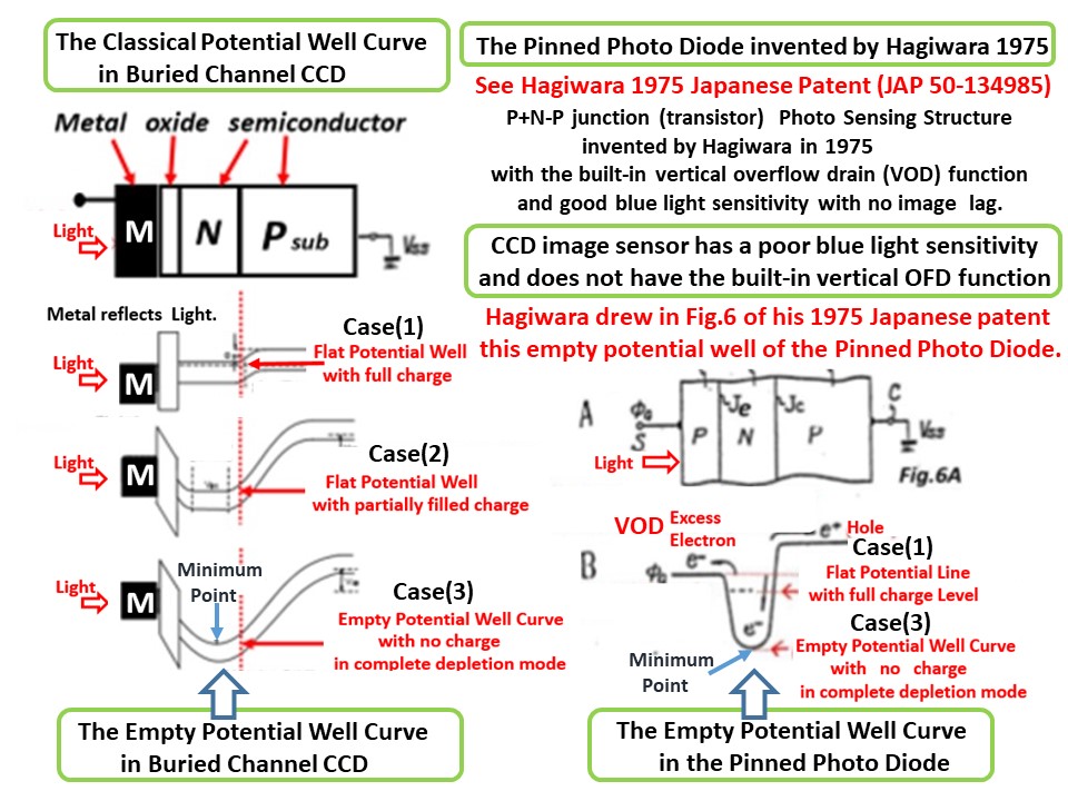
SONY-Fairchild Patent War ( 1991-2000) on Two Fairchild Patents.
Now, detailes of SONY-Fairchild Patent War ( 1991-2000) on Two Fairchild
Patents.
(1) the Amelio patent (USP3931674) about CCD fabrication process (USP3931674)
(2) the Early patent (USP3896485) about VOD in CCD photo detecting structure
In this SONY-Fairchild patent war, Fairchild asked SONY for more than
600 000 000 dollars patent fees for the SONY usage of the above two patents.
The truth is, SONY DID NOT use the above two patents in SONY CCD image
sensor products, but it was a very technically oriented and complecated device
physics problem was involved and very few people in the court really understood
how the CCD device is structured and how the CCD devices work at all.
Prof. Bob Bower of UC Davis as SONY Expert Witness helped SONY a lot
in the US courts against the two patents of Fairchild attacking SONY
image senosr business at that time
One is the Amelio patent (USP3931674) which was filed on Jan 13, 1976
on Self Aligned CCD Element including Two Levels of Electrodes and
Method of Manufacture therefore.
Actually, this Amelio patent was filed after the IEDM1973 paper,
“An Overlapped Electrode Buried Channel CCD” by D. M. Erb,
W. Kotyczka, S. C. Su, C. Wang, and G.Clough working for Hughes
Aircraft Company at that time.
Dr.Stephen C. Su , who was also once the president of Sharp Taiwan,
also helped as Expert Witness for Sony, reporting that Sony process
was based on the IEDM1973 paper by Hughes Aircraft Company.
In the lab notebook of D.M. Erb, Erb wrote that the true inventor
of the Ion Implanted Barrier Buried Channel CCD is Dr.S. C. Su.
Also as an Expert Witness, Anthony J Denboer, the vice president
of Integrated Circuit Engineering Corp as SEM, TEM Reverse
Engineering Expert reported in the court for SONY that
Sony CCD process was based on the IEDM1973 process and
nothing to do with the Amelio patent process (USP3931674).
Fairchild knew the Erb IEDM1973 paper but did not quote this
paper in the court, which was not fair.
Prof. Robert W. Bower as SONY Expert witness, based on more
than 250 pages of his prepared documents reported that Sony
process and Hughes Process are identical.
Prof. Robert W. Bower is a well-known semiconductor pocess
authority as one of the patent holders on the MOS Self Align
Ion Implantation.
So Fairchild lost the patent war on the Amelio patent against Sony.
The other is the Early patent (USP3896485) filed on July 22, 1975 on
“Charge Coupled Device with Overflow Protection.
This early patent is about the surface type CCD photo sensing part
with the buried N+ overflow drain which function as the vertical
over flow drain for excess signal charge (electrons) at very strong
light illuminations. This structure was Metal/Oxide/P/N+/Psub type
photo sensing element structure.
However, SONY HAD invented by Hagiwara is not the CCD sensor
type light detecting structure that was defined in the Early patent.
SONY HAD has the top P+ region of hole majority carrier accumulation layer.
SONY HAD is a thyristor-type photo sensing structure, which is actually
Oxide/P+/N/P/Nsub junction (thyristor) type photo sensing element structure
which was invented by Hagiwara in 1975 Japanese patent, however, which was
filed in November 10, 1975.
The problem is that Hagiwara 1975 patent on the SONY HAD was filed
later than Early 1975 patent by 4 months.
So Sony had to explain the court that these two structures are completely
different structures.
Sony argued that
(1) Sony HAD sensor have the Nsub as the draining Thyristor Collector Terminal
which is based on the Thyristor Punch thru action while Early patent has the N+
sink drain region, which is a region with a limited space.
Sony have the N-type substrate as the draining sink which is not a limited region.
Sony draining sink is the entire bottom part of the silicon die.
(2) SONY HAD Draining Sink is pinned to a fixed voltage from the substrate
contact ( which is now called Pinned Photo Diode with top P+ region connected
to the bottom P-well region ) while Early Patent Draining Sink is connected
derectly by the metal contact from the top silicon surface.
(3) The photo carrier storage region in SONY HAD is connected to the adjacent
charge transfer devices such as buried channel CCD via the single charge transfer
MOS type analog swichong gate and the signal charge in the buried N base region
never have contact to the SiO2/Si surface while in Early Patent the signal charge
is to be transported along the SiO2/Si surface inversion layer under the surface
type CCD type charge transfer electrodes in series.
Sony had a very hard time to convince these differences to the court people
who does not have the semiconductor physics background.
Nobody knew whether court people understood these confusing technical
differences. With some lost and win match due to this confusing technical
issues, Sony lost.
But at the end, after the underground detailed independent background
technical hearings and FBI investigations by court-side, the court judge
declared Sony victory by surprise.
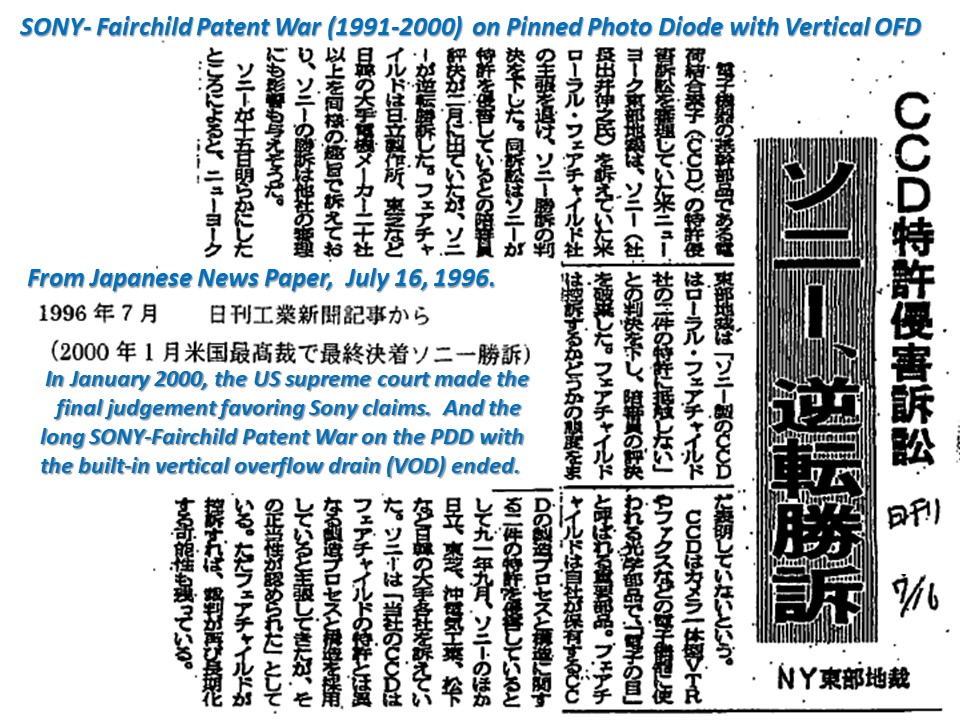
In this process I also published an IEEE paper on the SONY HAD, which
is now called Pinned Photo Diode to support SONY claims.
After the SONY victory in 2000, Ohga chairman and Idei president and
other SONY top executives gave me a simple thank-you message.
This documentation was dated on August 1, 1996 in which SONY Chairman Ohga
signed his own name with the " Thank you, Hagiwara-san ! " message.
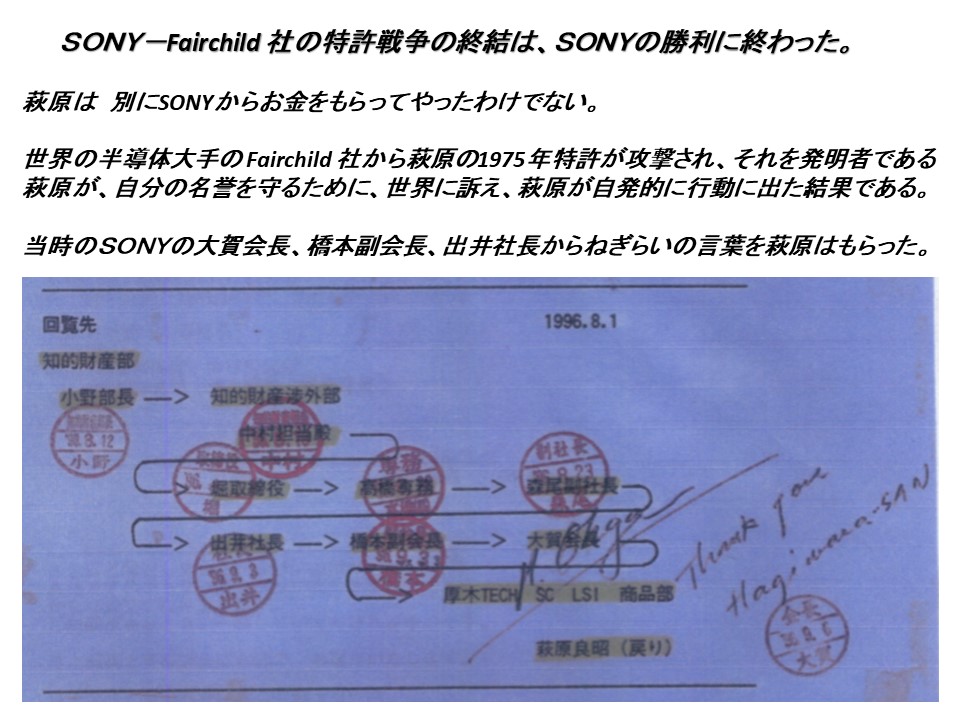
Finally after the Sony victory over the SONY-Fairchild Patent War on Hagiwara
Patent,
Hagiwara's image sensor works for SONY were recognized and Hagiwara was awarded
with the First Patent Prize in SONY in April 2001.
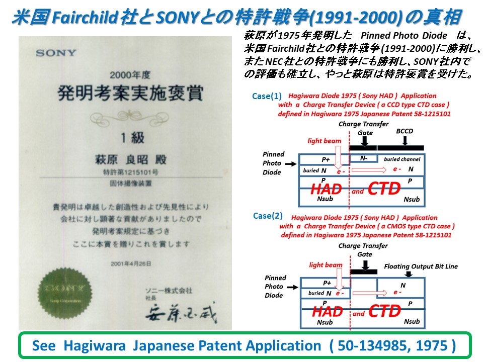
This Hagiwara 1975 patents on the Pinned Photo Diode helped SONY image
sensor
business for a long time, even now, since the SONY Press Conference in
Tokyo and
New York in 1978 which is shown on the top portion of the picture shown
below,
and also the SONY currect CMOS digital image sensor business shown on the
bottom
portion of the picture shown below for the thinned silicon die with back
light illumination.
Hagiwara had a very long bad time in Sony during the SONY-Fairchild Patent
War,
which lasted from 1991 till 2000. Sony top managements were all watching
silently
at the Sony-Fairchild war since it was a technical war on patents and they
cannot
contribute technically at all. These ten years years were lost years for Hagiwara.
He was like a prisoner in jail. He could not get out of the jail and could
not focus
his power on any responsible job positions in Sony until Sony finally achieved the
victory over the SONY-Fairchild Patent War on the Pinned Photo Diode that was
invented by Hagiwara at SONY in 1975.
Hagiwara 1975 invention saved and helped CCD image sensors on the high
lighted
stage for a long time from the behind curtain. Now still, Hagiwara 1975 invention
is helping CMOS digital mage sensors on the high lighted stage again from
the
behind curtain.
The world did not know these facts. And Hagiwara is now 70 yearsand feels
unhappy and lonely, wishing the world someday will know the true story
of
this Pinned Photo Diode since the world has the right to know the truth.
Now again, Hagiwara had to defend now his inventions because of
the Fossum 2014 fake paper in which Fossum claimes that
the pinned photo diode was invented by Tearanish ex-NEC engineer.
Prof. Albert Theuwissen wrote :
-----Original Message-----
From: hagiwara [mailto:hagiwara-yoshiaki@aiplab.com]
Sent: Tuesday, July 10, 2018 7:42 PM
To: 'albert theuwissen'
Cc: 'Yasuhiro.Ueda(SONY)' ; 'Terushi.Shimizu(SONY)'
Subject: Who is the Inventor of PPD ?
Albert, thank you for your e-mail.
>After some doubt I declined his (Fossum 2014 paper) invitation,
>because I do know that the discussion about the inventor of the PPD
>is very sensitive, and I do agree with you
>that the structure you developed is indeed a PPD,
>maybe not called that way at that time (1975 )
>and also invented for some other purpose (Vertical OFD) .
>But it still remains a PPD !
>At Philips, in the late '70s a very similar structure was implemented
>in the CCDs, this was before I joined Philips in 1983.
>So yes, there were several p+/n-/p- structures known by the time
>that Teranishi issued his patent. I fully agree to that.
Thank you very much for your kind comments.
from Yoshiaki Hagiwara
************************************************************
Fossum 2014 Fake Paper
************************************************************
It all started from the Fossum 2014 fake paper on Origin of Pinned Photo Diode.
************************************************************
Prof. Albert Theuwissen said that Fossum 2014 paper is doutful.
Prof. Akira Matsuzawa said that Fossum 2014 paper is fake.
Prof. Shingo Kagami said that SONY HAD ( which was invented by
Hagiwara in 1975 ) and the Pinned Photo Diode are the same thing.
The details of Hagiwara 1975 patents prove that Fossum is a big liar,
telling a big lie on the origin of Pinned Photo Diode.
Fossum said in his 2014 fake paper that Hagiwara 1975 Patent
invention did not describe any charge transfer operations,
which is a very, very big lie , deceiving the entire world,
including Queen Elizabeth of United Kingdom and also
the Emperor of Japan !!!!!!
The following two patents filed by Hagiwara at SONY
in 1975 clears shows that the two Hagiwara Patents
clearly define the Pinned Photo Diode structure with
the complete charge transfer operation mode.
************************************************************
Hagiwara Diode 1975 = Sony original HAD = Pinned Photo Diode.
************************************************************
Prof. Shingo Kagami of Tohoku University said that
SONY original HAD sensor and Pinned Photo Diode are the same thing.
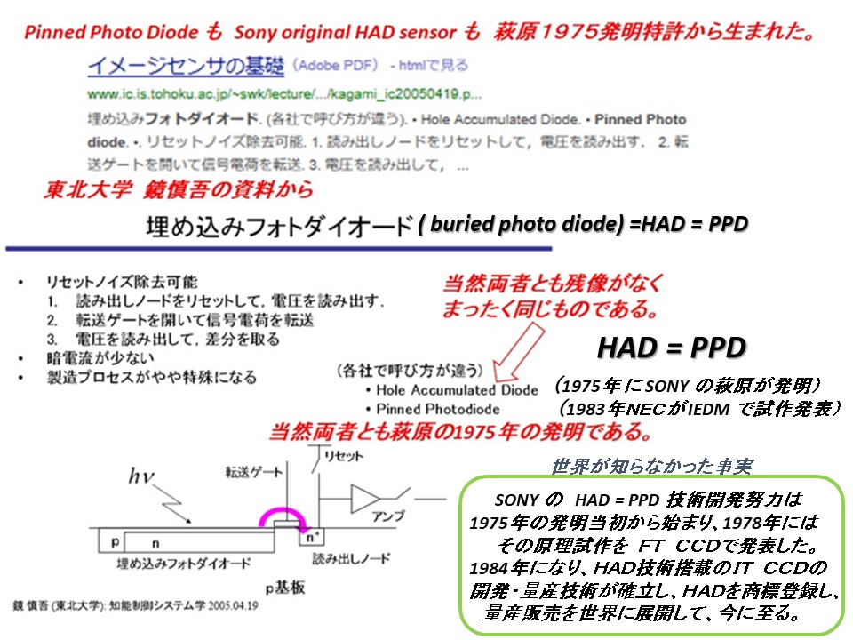
After the SONY victory on SONY-Fairchild Patent War ( 1991-2000),
SONY finally , recognized the works of, and awarded Yoshiaki Hagiwara,
as the inventor of SONY original HAD sensor which is also called as
Pinned Photo Diode worldwide.
The Japanese paper described about the SONY victory of SONY-Fairchild war
which was actually on the pinned photo diode patent, which is called in
SONY
by another name of SONY original HAD sensor.
Fairchild was attacking on the SONY products named as SONY original HAD
sensor,
which is the same thing as the pinned photo diode.
After working for the Sony Image Sensor Projects since 1975, Hagiwara worked
for the SONY 25nanosec Access
Time 4M bit Cache SRAM Project for quick picture caputurings of the modern digital camara system. He worked
for the SONY Playstation PS2 and PS3 Projects before retiring SONY in 2008
reaching at age 60.
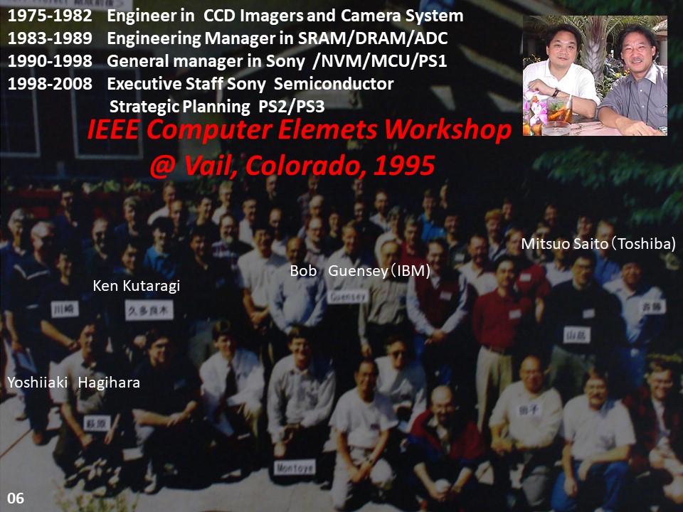
From 2008 to 2017, Hagiwara served as the president of the AIPS consotium, an NPO sponsored by Kanagawa-ken, Japan.
The AIPS consortium is a non-profit organization for Artificial Intelligent
Partner System including the inleligent image
sensor systems, smart game machine systems, and human friendly robot sysytems
like SONY AIBO.
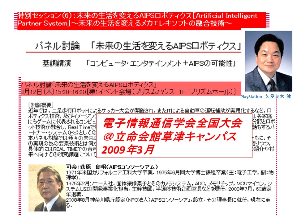
Hagiwara was educated in CalTech, California Institute of Technology in
Pasadena, California USA.
Prof.C.A.Mead, Prof.T.C.McGill and Prof.James McCaldin were his mentors.
The founder of Intel Corporation, Dr. Gordon Moore was also a CalTech graduate.
Gordon Moore knew Prof.C.A.Mead, Prof.T.C.McGill and Prof.James McCaldin
very well, and
they were friends and advisers each other who met each other very often
in Caltech and
in Intel. Hagiwara was a graduate student of Prof.C.A.Mead CalTech Lab
which is in the
Gordon Moore Laboratory of Electric and Elecronic Enginneerings in CalTech.
CatTech and Intel had a VLSI Design Project in 1971 to 1973. Hagiwara was
one of the
memebers of the VLSI Design Project and design the 128-bit Multicaomparator MOS
technology silicon chip, which was fabricated in Intel by CalTech graduates working for
Intel. The design team included Hagiwara evaluated the silicon chip in
CalTech and
later the work was published in IEEE Journal of Solid State Circuits, VOL.SC-11,
NO.4,
October 1975. The picture below shows Prof.C.A.Mead and Yoshiaki (Daimon)
Hagiwara
working on the 128 -bit Multicomparator VLSI Chip Desin Project in CalTech.
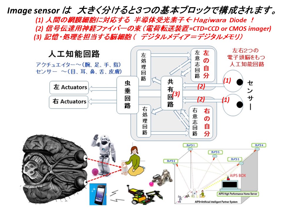
The below is in Japanse., but will be translated into English in near furure.
****************************************
Hagiwara at Sony is the true inventor of Pinned Photo Diode.
https://patents.justia.com/inventor/yoshiaki-hagiwara
Pictures of Pinned Photo Diode invented by Hagiwara in Patnet 1975
****************************************
萩原1975年特許 ( pinned photo diode Patent 1975) の解説
萩原1975年特許 ( pinned photo diode Patent 1975) の原文
萩原1975年特許( pinned photo diode Patnet 1975 )の画像
****************************************
***********************************************
Please judge yourself if the story is a truth or a fiction ?
***********************************************
Story of Sony original HAD sensor (1)
More Story (1) , Story(2), Story(3)
Story of Sony original HAD sensor (2)
Story of Sony original HAD sensor (3)
Story of Sony original HAD sensor (4)
Story of Sony original HAD sensor (5)
Story of Sony original HAD sensor (6)
Story of Sony original HAD sensor(7)
Story of Sony original HAD sensor(8)
***********************************************
**********************************************************************
Important Contributions for Image Sensor Developmet Efforts before 1975
**********************************************************************
J.Bardeen and W.H.Brattain, "Transistor: A Semiconductor Triode",
Physical Review, VOl.74, p.230, July 1948.
W.Shockley, "The theory of p-n Junction in Semiconductor and p-n
Junction Transistor", Proc. IEEE Vol.51, pp.1190-1202, September 1949.
S.R.Hofstein and F.P.Heiman, "The Siliocn Insulated-Gate Field Effect
Transistor", Proc. IEEE Vol.51, pp.435-1202, September 1963
Gordon E. Moore, "Cramming more components onto integrated circits",
Electronics,
Vol.38, No.8, April 19, 1965.
M.A.Schuster and G.Strull, " A Monolithic Mosaic of Photo Sensors for Solid
State Imaging Application", IEEE Trans. Electron Devices, Vol.ED-13, No.12, 1966
A. S. Grove, “Physics and Technology of Semiconductor Devices,”
John Wiley and Sons, Inc., New York pp.136-140, no.267, 1967.
P.K.Wiener, et al "A self-Scanned Solid State Image Sensor", in Proc. IEEE,
Vol 55, No.9, 1967.
G.P.Weckler, "Operation of PN Junction Photo Detectors in a Photon Flux
Integrating Mode", IEEE J. Solid State Circuits. Vol2, pp.65-73, September 1967.
P.J.W. Noble, "Self-Scanned Silicon Image Dector Arrys", IEEE Trans. Electron
Devices, Vil.ED-15, No.4, pp.202-209,1968.
S.G. Chamberlain, "Photosensitivity and Scanning of Silicon Image Detector
Arrays" IEEE J.Solid State Circuits, Vol.SC-4, No.6, pp.333-342, 1969.
F.L.J.Sangster and K.Teer, "Bucket Brigate Electronics - New Possibilities
for Delay Time-Axis Conversion and Scanning", IEEE J.Solid-State Circuits,
VOl.SC-4, No.3, pp.131-136, 1969.
W. S. Boyle and G. E. Smith, “Charge-Coupled Semiconductor Devices,”
Bell Syst. Tech. J., 49, pp.587-593, 1970.
W.M.Regitz and J.Karp, "A Three-transistor-cell, 1024 bit, 500 nsec
MOS RAM", ISSCC1970, Feb. 1970
F.L.J. Sanger, "Integrated MOS and Bipolar Analog Delay Lines using
Bucket Brigate Capacitor Storage", ISSCC1970, pp.74-75, 185, Feb. 1970.
G.F.Amelio, M.F.Tompsett and G.E.Smith, "Experimantal Verification of the
Charge Coupled Semiconductor Devices", B.S.T.J.Vol.49,pp.587-593,Apr. 1970
W.M.Regitz and J.Karp, "A Three-transistor-cell, 1024 bit, 500 nsec
MOS RAM", IEEE JSSC, VOl.SC-5, No.5, pp.181-186, October 1970.
W.F.Kosonocky and J.G.Carns, " Charge Coupled Digital Circuits", ISSCC1971,
pp.161-163, February 1971
G. F. Amelio, W. J. Bertram, Jr., and M. F. Tompsett,
“Charge-Coupled Imaging Devices: Design Considera- tions,”
IEEE Trans. Electron Devices, ED-18, no.11, pp.986-992, 1971.
M.F.Tompsett, et al "Charge Coupled Imaging Devces Experimental Results",
IEEE Trans. Electron Devices, Vol. ED-18, No.11, pp.992-996, 1971.
J.E.Carnes, "Drift-Aiding Fringing Fields in Charge Coupled Devices", IEEE J.
Solid State Circuits, Vol.SC-6, No.5, pp.322-326, 1971.
W.F.Kosonocky and J.G.Carns, " Charge Coupled Devices" ISSCC1972,
pp.132-133, February 1972.
C.H.Sequin, "Blooming Supression in Charge Coupled Area Imaging" Bell Sys.
Tech. J., 51, oo. 1923-1926, 1972.
J.D.Plummer and J.D.Meindl, " A Low-Light-Level Self-Scanned MOS Image
Sensor" ISSCC1972 Dig.Tech.Paper pp.30-31, February 1972.
J. E. Carnes and W. F. Kosonocky,
“First Interface-State Losses in Charge-Coupled Devices,”
Appl. Phys. Lett., vol.20, pp.261-263, 1972.
J. E. Carnes and W. F. Kosonocky,
“Noise Sources in Charge-Coupled Devices,”
RCA Review, vol.33, pp.327-343, 1972.
R. H. Walden, R. H. Krambeck, R. J. Strain, J. McKenna,
N. L. Schryer, and G. E. Smith, “The Buried Channel Charge
Coupled Devices,” Bell Syst. Tech. J., no.51, pp.1635-1640, 1972.
G. F. Amelio, “Physics and Applications of Charge Coupled Devices,”
IEEE INTERCON, New York, Digest, vol.6, paper 1/3, 1973.
D. M. Erb, W. Kotyczka, S. C. Su, C. Wang, and G. Clough,
“An Overlapping Electrode Buried Channel CCD,”
IEDM, Washington, D.C., Tech. Digest, pp.24-26, 1973.
W. F. Kosonocky and J. E. Carnes,
“Two Phase Charge Coupled Devices with Overlapping Polysilicon
and Aluminum Gates,” RCA Review, vol.34, pp.164-202, 1973.
D.M.Erb,W.Kotyczka, S.C. Su, C.Wamg and G.Clough, "An Overlapped
Electrode Buried Channel CCD", IEDM1973, Dec 3-5, 1973.
S. R. Shortes et al., “Development of a thinned backsideilluminated
charge-coupled device image,” in Proc. IEDM1973, Dec. 1973, p. 415.
N.G. Vogi, et al "A Half-Million Pel Bucket Brigate Optical Scanner",
ISSCC1974, pp. 30-31, February 1974.
P. A. Gray and H. Coltman, “Back surface imaging of thinned CCDs,”
in Proc. CCD, 1974, pp. 162?167.
J. Lohstroh, "The JFET as a Photosensitive Cell in Image Sensor Arrys",
ISSCC1974, pp. 34-35, February 1974.
M.H. White, "Characterization of Surface CHannel CCD Image Arrays at
Low Light Level", IEEE J. Solid State Circuits, Vol.SC-9, No.1, pp.1-12, 1974.
A. W. Lees and W. D. Ryan, “A Simple Model of a Buried-Channel
Charge-Coupled Device,” Solid-State Electron., vol.17, pp.1163-1169, 1974.
C. H. Sequin, F. J. Morris, T.A. Shankoff, M. F. Tompsett, and E. J. Zimany,
“Charge-Coupled Area Image Sensor Using Three Levels of Polysilicon,”
IEEE Trans. Electron Devices, ED-21, pp.712-720, 1974.
M. H. White, D. R. Lampe, F. C. Blaha, and I. A. Mack,
“Characterization of Surface Channel CCD Imaging Arrays
at Low Light Levels,” IEEE Trans. Solid-State Circuits,
SC-9, pp.1-13, Feb. 1974.
D. F. Barbe, “Imaging Devices Using the Charge-Coupled Concept,”
Proc. IEEE, vol.63, no.1, pp.38-67, 1975.
C. H. Sequin and M. F. Tompsett, “Charge Transfer Devices,”
Academic, New York, 1975.
James M. Early ( Fairchild Camera and Instrument Corporation, USA ) "Charge
Coupled Device with Overflow Protection", USP 3896485, July 22, 1975.
Hagiwara
had to protect his 1975 Japanese patent ( 1975-127647 ) on the P+NPNsub
Junction (Thyristor ) type Light Detecting Picture Cell Structure agaist
this
Fairchild Early USP 3896485 patent. The SONY-Fairchild Patent War lasted
from
1991 till 2000. Finally, Sony won the Patent war over Fairchild. But during the
long period of 10 years, Hagiwara felt as if he was in Jail and could not
perform
any important job tasks in Sony at all.
*************************************************************
Hagiwara Contributions for Image Sensor Developmet Efforts
*************************************************************
Hagiwara ISSCC1974 Paper on "Buried Channel CCD Charge Transfer"
February 1974 in Philadelphia, USA. This was Hagiwara PhD thesis paper
at California Institute of Technology (CalTech) Pasadena, California USA>
Hagiwara, 1975 Japanese Patent ( JA 1975-127647 ) at SONY
on the Pinned Photo Diode with Back Light Illumination
Hagiwara, 1975 Japanese Patent ( JA 1975-134985 ) at SONY
on the Pinned Phodo Diode with Vertical Overflow Drain Function
C.A.Mead, R.D.Pashley,Lee D. Britton, Yoshiaki T.Daimon Hagiwara and
S.F. Sando, "128-Bit Multicomparator", J. Solid State Circuits, Vol.SC-11,
No.5, October 1976. This is important for intelligent image sensor systems.
Hagiwara, 1978 Solid State Semiconductor Device Conference Paper on
"Narrow Channel Frame Transfer CCD Image Sensor" at Tokyo, Japan .
This is the first paper in the world reporting the P+NP type ( dynamic
PNP junction ( photo transistor ) type light detecting picture element
structure, which was later called as the Pinned Photo Diode.
Y. Daimon-Hagiwara, M. Abe, and C. Okada, “A 380Hx488V CCD imager
with narrow channel transfer gates,” Japanese J. Appl. Phys., vol. 18,
supplement 18?1, pp. 335?340, 1979.
Hagiwara, CCD'79 invited paper on "SONY Image Sensor Efforts"
at Edinburgh, Scotland UK on SONY CCD image sensors.
Fumio Miyaji, Yasushi Matsuyama, Yoshikazu Kanaishi, Katsunori Senoh,
Takashi Emori and Yoshiaki Hagiwara, "A 25 nanosec 4 Mega bit CMOS
RAM with DYnamic Bot-Line Loads", ISSCC1989 and J.Solid State Circuits,
Vol24, No.5, October 1989. This wad for Cache SRAM memory for SONY
Compact Digital CCD Image Sensors.
Y. Hagiwara, “High-density and high-quality frame transfer CCD imager
with very low smear, low dark current and very high blue sensitivity,”
IEEE Trans. Electron Devices, vol. 43, no. 12, pp. 2122?2130, Dec. 1996.
Hagiwara, ESSCIRC2001 invited paper on "SONY Consumer Electronics"
at Vilach, Austria
Hagiwara, ESSCIRC2008 invited paper on "SOI Cell Processor and Beyond"
at Edinburgh, Scotland UK
Hagiwara, the 60th Aniversary ISSCC2013 Plenary Panel Talk,
at San Franicisco, USA
***************************************************************************
Important Contributions for Image Sensor Developmet Efforts after 1975 and later.
***************************************************************************
Gilbert F. Amelio ( Fairchild Camera and Instrument Corporation, USA )
"Self Aligned CCD Element including Two Levels of Electrondes and
Method of Manufacture therefor" USP 3931674, Jan 13, 1976.
This Amelio patent (USP3931674) which was judged invalid by the prior
art of USP3745647 by Boleky and by IEDM1973 paper by D.M.Erb,
W.Kotyczka, S.C.Su, C.Wamg and G.Clough, "An Overlapped Electrode
Buried Channel CCD", IEDM1973, Dec 3-5, 1973.
T. Yamada, H. Okano, and N. Suzuki, “The Evaluation of Buried Channel Layer
in BCCD’s,” IEEE Trans. Electron Devices, ED-25, no.5, pp.544-546, 1978.
J. Hynecek, “Virtual phase CCD technology,” in Proc. IEDM1979, pp. 611?614,
Dec. 1979,
J.Nishizawa, et al, "Static Induction Transistor Image Sensors", IEEE Trans.
Electron Devices, Vol.ED-26, No.12, pp.1970-1977, 1979.
A. Furukawa, Y. Matsunaga, N. Suzuki, N. Harada, Y. Endo, Y. Hayashimoto, S. Sato,
Y. Egawa, and O. Yoshida, “An Interline Transfer CCD for A Single Sensor 2/3” Color
Camera,” IEDM, Washington, D. C., Tech. Digest, pp.346-349, 1980.
K.Hoshi, T.Suzuki, Y.Okubo and N.Isawa, "CZ Siliocn Crystal grown in Transverse
Magnetic Fields", 157th ECS Mtg Ext. Abstract, pp.811-813, May 1980.
T.Asada and F.Nagumo, "A New CCD Digital Color Camera using Direct Encoding
Method", Int. Conf. on Digital Signal Processing, September 2-5, 1981, Florence Italy.
Y. Ishihara, E. Oda, H. Tanigawa, N. Teranishi, E. Takeuchi, I. Akiyama, K. Arai,
M. Nishimura, and T. Kamata, “Interline CCD Image Sensor with an Anti Blooming
Structure,” ISSCC Digest of Technical Papers, pp.168-169, Feb. 1982.
N. Teranishi, A. Kohno, Y. Ishihara, E. Oda, and K. Arai, “No Image Lag Photodiode
Structure in the Interline CCD Image Sensor,” IEDM Tech. Dig., pp.324-327, 1982.
Y.Ishihara and K.Tanigaki,"A High Photosensitivity IL-CCD Image Sensor with
Monolithic Resin Lens Array", IEDM1983 Tech. Dig, pp.497-500, December 1983.
B.C. Burkey et al, "The Pinned Photo Diode for an Interline Transfer Image Sensor",
IEDM1984, DIg.Tech.Papers, pp.28-31, December 1984.
K. Horii, T. Kuroda, and S. Matsumoto, “A New Configuration of CCD Imager with a
Very Low Smear Level -FIT-CCD Imager,” IEEE Trans. Electron Devices, ED-31, no.7,
pp.904-909, 1984.
Y. Matsunaga and N. Suzuki, “An Interline Transfer CCD Imager,” ISSCC Digest of
Technical Papers, pp.32-33, Feb. 1984.
M.Ogawa et al, "Signal-PRocesiing ICs employed in a Single-Chip CCD Color Camera",
IEEE TRansaction on Consumer Electronics, Vol.CE-30, No.3, pp.374-381, Aug.1984
T.Kumezawa et al, "High Resolution CCD Image Sensors with Reduced Smear", IEEE
transaction on Electron Devices, VOl. ED-32, No.8, pp.1451-1456,1618, Aug. 1985.
Y.Ogawa et al, "Development of CCD Imaging Block for Single Chip Color Camera",
IEEE Transaction on Consumer Electronics, Vol.CE-31, No.3, pp.405-413, Aug. 1985
T.Nakamura,"A New MOS Image Sensor Operating in a Non-destructive Readout
Mode", IEDM1986, Tech.Dig. pp.353-356, December 1986.
M.Yamamura et al, "A 1/2 inch CCD Imager with 510 x 492 pixels", SPIE Vol.765
Image Sensors and Displays pp.41-46, Jan 13-14, 1987.
T. Yamada, K. Ikeda, and N. Suzuki, “A Line-Address CCD Image Sensor,”
ISSCC Digest of Technical Papers, pp.106-107, Feb. 1987.
T. Yamada, T. Yanai, and T. Kaneko, “2/3 Inch 400,000 Pixel CCD Area Image Sensor,”
Toshiba Review, no.162, pp.16-20, Winter 1987.
N. Teranishi and Y. Ishihara, “Smear Reduction in the Interline CCD Image Sensor,”
IEEE Trans. Electron Devices, ED-34, no.5, pp.1052-1056, 1987.
A.J.P.Theuwissen et al, "A 400K Pixel 1/2 inch Accorion CCD Imager", ISSCC1988,
Dig.Tech.Papers, pp.48-49, February 1988.
M. Hamasaki, T. Suzuki, Y. Kagawa, K. Ishikawa, M. Miyata, and H. Kambe,
“An IT-CCD Imager with Electronically Variable Shutter Speed,” ITEJ Technical
Report, vol.12, no.12, pp.31-36, 1988.
H.Yamashita et al, "A New High Sensitivity Photo-transitor for Area
Image Sensors", IEDM1988 Tech Dig pp.353-356, December 1988.
J.Hynecek, "A New Device Architecture Suitable for High-Resolution
and High Performance Image Sesnors", IEEE Trans, Electron Devices,
Vol.35, No.5, pp.646-652, 1988.
N.Tanaka, et al,"A Novel Bipolar Imaging Device with Self-NOise Reduction
Capability", IEEE Trans. Electron Devices, Vol.36, No.1, pp.31-38, 1989
K.Yonemoto et al, "A 2 million Pixel FIT-CCD Image Sensor for HDTV
Camera System" IEEE ISSCC1990, pp.214-216, February 1990.
F.Andoh et al,"A 250 000 Pixel Image Sensor with FET Amplification
at Each Pixel for High Speed Television Cameras", ISSCC1990, Dig.Tech.Papers
pp.212-213, February 1990.
Eric G. Stevens et al, "A One Mega Pixel Progressive Scan Image Sensor with
Antiblooming Control and Lag-Free Operation", IEEE Trans. Electron Devices,
Vol38, No.5, pp.981-988, 1991.
K.Ishikawa and T.Iizuka, "One inch 2M pixel CCD with Hyper HAD sensor and
Camera System for HDTV", SPIE proc. Vol. 1656, pp.30-40, February 1992.
T. Ishigami, A. Kobayashi, Y. Naito, A. Izumi, T. Hanagata, and K. Nakashima,
“A 1/2-in 380k-pixel Progressive Scan CCD Image Sensor,” ITE Technical Report
Vol.17, no.16, pp.39-44, Mar. 1993.
P.B.Denyer et al, "CMOS Image Sensors for Multimedia Applications", IEEE
Constum Integrated Circuits Conference 1993, Proc. of CICC1993,
pp.11.5.1-11.5.4, 1993.
H.Kawashima et al, "A 1/4 inch Format 250K Pixel Amplified MOS Image Sensor
Using CMOS Process", IEDM1993, Tech. Dig. pp.575-578, December 1993.
S.K.Mendis et al, "128 x 128 CMOS Active Pixel Image Sensor for Highly Integrated
Imaging Systems", IEDM1993, Tech. Dig. pp.583-586, December 1993.
E.R.Fossum,"Active Pixel Sensors: Are CCD's dinosaurs ?" , in Proc. SPIE,
Vol.1900, pp.2-14, 1993.
Hitachi MOS Image Sensor Engineers and Intel MOS Process Engineers all
knew
that eventually scaled down MOS Process Technology will conquer all other
kinds of Process Technologies including CCD image sensor technology because
of the power consideration and scaled down dimensional advantage of CMOS
process technology. The three transistor CMOS active picture cell was already
invented as, since the three-transistor circuit is identical to, the three-transitor
circuit of the DRAM cell with the active source follower type current amplification.
Fossum was just a commentator in his SPIE 1993 paper above, emphasizing
the fact
and speculations that the original image sensor experts and engineers all
knew in 1970s.
R.H.Nixon et al, "128 x 128 CMOS Photodiode Type Active Pixel Sensor
with On-ChipTiming Ccntrol and Signal CHain Electronics", in Proc. SPIE,
Vol.2415, pp.117-123, 1995.
S. Kawai et al, "Photo Response Analysis in CCD Image Sensors with a VOD
Structure", IEEE TRans. Electron Devices, VOl.42, No.4, pp.652-655, 1995.
Paul P. K. Lee et al, "An Active Pixel Sensor Fabricated Using CMOS/CCD
Process Technology", in Proc. IEEE Workshop on CCDs and Advanced
Image Sesnors", 1995.
S.Kawahito et al,"A Compressed Digital Output CMOS Image Sensor with
Analog 2-D DCT Processors and ADC/Quantizer",ISSCC1997, Dig.Tech.Papers,
pp.184-185, February 1997.
T. H. Lee, R. M. Guidash, and P. P. Lee, “Partially pinned photodiode
for solid-state image sensors,” U.S. Patent 5,903,021, Jan. 1997.
R. M. Guidash, “Active pixel image sensor with shared ampli?er
readout,” U.S. Patent no. 6,107,655, Aug. 1997.
Walter F. Kosonocky et al, "360 x 360 Element Three-Phase Very High
Frame Rate Burst Image Sesnor, Design, Operation and Perfomance",
IEEE Trans. Electron Devices, Vol.44, No.10, pp.1617-1624, 1997.
R.M.Guidash et al, "A 0.6 um CMOS Pinned Photo Diode Color Imager
Technology", IEDM1997, Tech. Dig. pp.927-929, December 1997.
M.Loinaz, et al, "A 200mW 3.3V CMOS Color Camera IC Producing
352 x 288 24b Video at 30 Frames/sec", ISSCC1998, Dig.Tech.Papers,
pp.168-169, February 1998.
Guang Yang, Orly Yadid-Pecht, Chris Wrigley, and Bedabrata Pain ,
"A Snap-Shot CMOS Active Pixel Imager for Low-Noise, High-speed
Imaging", IEDM1998, December 1998.
F.Andoh et al, "A Digital Pixel Image Sensor with 1 bit ADC and
8 bit Pulse Counter in Each Pixel", International Image Sensor
Workshop, P1, 1999.
K. Yonemoto et al, "A CMOS Image Sensor with a Simple FPN
Reduction Technology and a Hole Accumulation Diode", ISSCC2000,
Dig.Tech.Papers, pp.102-103, February 2000.
T. Yamada, Katsumi Ikeda, Y. G. Kim, H. Wakoh, T. Toma, T. Sakamoto,
K. Ogawa, E. Okamoto, K. Masukane, K. Oda, and M. Inuiya, “A progressive
Scan CCD Image Sensor for DSC Applications,” IEEE J. of Solid-State
Circuits, vol.35, no.12, pp.2044-2054, 2000.
M.Furuyama et al,"High Sensitivity and No Crosstalk Pixel Technology
for Embedded CMOS Image Sesnor", IEEE Trans. Electron Devices,
Vol.48, No.10, 2001.
T.Miida,"A 1.5 M Pixel Imager with Localized Hole-Modulation Method",
ISSCC2002, Dig.Tech.Papers, pp.42-43, February 2002.
T. GOji Etoh,"A CCD Image Sensor of 1Mframe/sec for Continuous
Image Capturing 103 Frames", ISSCC2002, Dig.Tech.Papers, pp.46-47,
February 2002.
T.Sugiyama et al, "A 1/4 inch QVGA Color Imaging and 3-D Sensing
CMOS Sensor with Analog Frame Memory", ISSCC2002,Dig.Tech.Papers,
pp.434-435, February 2002.
A. Theuwissen, "50 years of Solid State Image Sensors",
ISSCC2003, Dig.Tech. Papers, S26, February 2003.
I. Inoue et al., “Low-leakage-current and Low-operating-voltage
Buried Photodiode for a CMOS imager,” IEEE Trans. Electron Devices,
vol. 50, no. 1, pp. 43?47, Jan. 2003.
K.Mabuchi,N.Nakamura, E.Funatsu,T.Abe,T.Umeda,T.Hoshino,R.Suzuki,
H.Sumi, "CMOS Image Sensor Using a Floating Diffusion Driving Buried
Photo Diode", ISSCC2004, pp.112-113, February 2004.
H.Takahashi et al, "A 3.9 um Pixel Pitch VGA Format, 10 bit Digital
Image Sensor with 1.5 Transistor /Pxcel", ISSCC2004, pp.108-109, Feb. 2004.
M.Mori et al, "A 1/4 inch 2M Pixel CMOS Image Sensor with 1.75
Transistor/Pixel", ISSCC2004, pp.110-111, February 2004.
Nana Akahane, Rie Ryuzaki, Satoru Adachi, Koichi Mizobuchi,
Shigetoshi Sugawa, "A 200dB Dynamic Range Iris-less CMOS Image
Sensor with Lateral OverflowIntegration Capacitor using Hybrid Voltage
and Current Readout Operation", ISSCC2006, pp.300-301, Feb.7, 2006.
Shin Iwabuchi et al,"A Back illunated High Sensitivity Small Pixel
Color CMOS Image Sensor with Flexible Layout of Metal Wiring",
ISSCC2006, pp.302-303, Feb.7, 2006
Y. Nitta et al, "High Speed Digital Double Sampling with Analog CDS
on Column parallel ADC Architecture for Low Noise Active Pixel Sensor",
ISSCC2006, pp.500-501, Feb. 8, 2006
S.Yoshihara et al, "A 1/1.8 inchi 6.4 Mega Pixel 60 frames/sec CMOS
Image Sensor with Seamless Mode Change", ISSCC2006, Dig.Tech.Papers
pp.1984-1993, February 2006.
K.Cho et al, " A 1/2.5 inch 8.1 Mega Pixel CMOS Image Sesnor for
Digital Camera",ISSCC2007, Dig.Tech.papers pp.508-509, February 2007.
S-H Cho et al, "Optoelectronic Investigation for High Performance 1.4 um
pixel CMOS Image Sensors", International Image Sensor Workshop (IISW2007),
June 6-10, 2007.
Xinyang Wang, Padmakumar R.Rao, and Albert J.P. Theuwissen,
"Characterization of the Buried CHannel NMOS Source Followers
in CMOS Image Sesnors", International Image Sensor Workshop
(IISW2007), June 6-10, 2007.
Shoji Kawahito and Nobuhiro Kawai, "Column Parallel Signal
Processing Techniues for Reduing Thermal and RTS Noises in
CMOS Image Sensors", International Image Sensor Workshop
(IISW2007), June 6-10, 2007.
G.Agranov et al, "Super Small Sub 2 um Pixels for Novel CMOS
Image Sensors", International Image Sensor Workshop (IISW2007),
June 6-10, 2007.
J.Prima et al, "A 3 Mega Pixel Back illuminated Image Sensor
in 1T5 Architecture with 1.45 um Pixel Pitch", International
Image Sensor Workshop (IISW2007), June 6-10, 2007.
B.Cremers et al, "A High Speed Pipelined Snapshoto CMOS Image
Sensor with 6.4 Gpixel/sec Data Rate", International Image Sensor
Workshop 5.9, p.9, 2009.
K.Itonaga et al, "Extremely Low Noise CMOS Image Sensor
with High Saturation Capacity", IEDM2011, Dig.Tech.Papers
pp.171-174, December 2011.
M.Sakakibara et al,"An 83 dB Dynamic Range Single Exposure Global
Shutter CMOSImage Sensor with In-Pixek Dual Storage", ISSCC2012,
Dig.Tech.Papers, 22.1, pp.380-381, February 2012.
T.Tochigi et al, "A Global Shutter CMOS Image Sensor with Readout
Speed of One Tpixel/secBurst and 780 Mpixel/sec Continuous",
ISSCC2012, Dig.Tech.Papers, 22.1, pp.382-384, February 2012.
E.R.Fossum and D.B.Hondongwa, " A Review of the Pinned Photo Diode
for CCD and CMOS Image Sensors", IEEE J. of Electron Devices Society,
VOL-2, No.3, May 2014. This is a fake paper which did not quote the
Hagiwara 1975 patent on the Back Light Illuminated Pinned Photo Diode
Light Detecting Element Structure ( 1975-127647 ) with the complete
charge transfer operation mode with the image lag free feature. This
Fossum fake 2014 paper made also many false statements on the Hagiwara
1975 patent on the P+NPNsub junction (thysitor) type Pinned Photo Diode
Light Detecting Element Structure ( 1975-134985 ) that has the complete
charge transfer action with no image lag feature, and also with the built-in
vertical overflow drain (VOD) function.
***********************************************************************
***********************************************************************
*******************************************************************
Digital CMOS Image Sensor is watching at its inventor, Yoshiaki Hagiwara.
Hagiwara is the Inventor of SONY HAD and Pinned Photo Diode Image Sensors.
*******************************************************************
**********************************
Please purchase and read
"The world of Digital Circuit Systems
that supports the artificial intelligent
partner systems (AIPS). " wrote in
Japanese by Yoshiaki Hagiwara in 2016.
ISBN 978-4-88359-339-2 C3055
Price 9000 Japanse Yen and TAX.
B5 size Hard Cover 475 pages
Publisher Seizansha_Inc
Tel +81-42-765-6460
https://www.seizansha.co.jp/ISBN/ISBN978-4-88359-339-2.html
*************************************
return to http://www.aiplab.com
**************************************