*******************************************************************************
Hagiwara at Sony is the true inventor of Pinned Photo Diode
Pinned Photo Diode was invented by Hagiwara of Sony in 1975
******************************************************************************
hagiwara-yoshiaki@aiplab.com
*******************************************************************
See also ElectronicsStackExchangeSite on What is Pinned Photo Diode ?
Hagiwara at Sony is the true inventor of Pinned Photo Diode.
Pinned Photo Diode was invented by Hagiwara of Sony in 1975
Story of Pinned Photo Diode
*******************************************************************
*******************************************************************
See three invited talks related to SONY HAD sensor now called also as Pinned
Photo Diode.
(1) International Conference CCD79 in Edinburgh, Scotland UK
(2) International Conference ESSCIRC2001 in Vilach, Austria.
(3) International Conference ESSCIRC2008 in Edinburgh, Scotland UK
*******************************************************************
Hagiwara was invited in these international conferences because of his
contributions
to the image sensor community and related digital system LSI chip design
works.
*******************************************************************
*******************************************************************
Brief History of Image Sensors.
*******************************************************************
In 1960s, before CCD was invented, we already had beautiful color pictures
by the classical MOS image sensor with an excellent light sensitivity obtained
by the classical N+P junction type photo diode.
But to overcome the very large wire (CkT) noise, the three transistor
active source follower type circuits, invented by Peter Noble, was needed.
But the picture cell area was too small to incorporate this active circuit
in each picture cell area. We all knew that we had to wait untill we have
the complete MOS transistor process scale down, much furthur down.
(2) However, the CCD invention gave the image lag free and very low
wire (CkT) noise pictures. The CCD became the super star with the
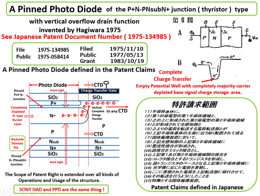
help of the P+NPNsub junctiion (thyrsitor) type photo diode, which
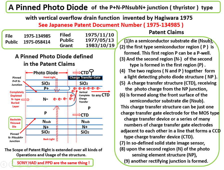
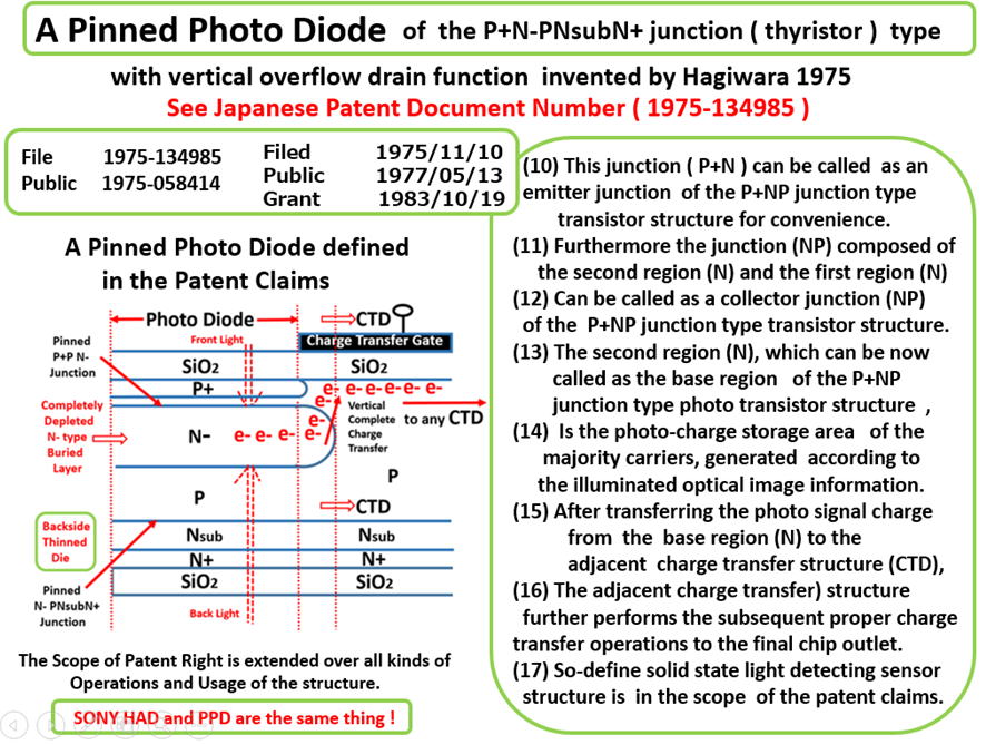
was invented by Hagiwara in 1975. See JAP ( 1975-134985 ) .
CCD consumed a lot of power with only the transfer efficency of 99.999
%,
which was however possible to be applied for the classical NTSC picture
resolution. CCD had the serious trap noise and surface dark current problems.
Moreover, CCD had inherently MOS metal-type electrodes that do not pass
light and CCD was not as light-sensitive as the N+P photo diode. So, the
CCD
type light detecting picture cell was replaced by the the P+NPNsub junctiion
(thyrsitor) type photo diode, Hagiwara 1975 invention. See JAP ( 1975-134985 ) .
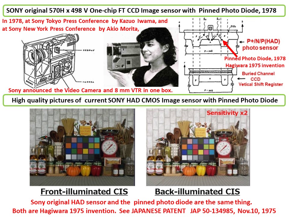
In 1978, SONY annouced in New York and Tokyo Press Conferences the world
first CCD image sensor with no image lag, very highly light sensitive,
low trap
noise, low surface dark current features of the PNP junction type photo
diode
sensor pixel structure,Hagiwara 1975 invention. See JAP ( 1975-134985 ) .
At that time, the world already gave up the CCD image development efforts.
SONY was the only company that never gave up. Sony showed the future of
CCD image sesnor applications. The truth is that Hagiwara in SONY was the
only engineer in the world who did not give up. And Hagiwara showed the
future of CCD image sesnor applications. by the P+NPNsub junctiion type
photo diode, Hagiwara 1975 invention. See JAP ( 1975-134985 ) .
So Hagiwara save the CCD by his 1975 invention, which is now called by
another name, the Pinned Photo Diode.
The truth is that CCD was NOT highly light sensitive, NOT low dark current
and NOT trap noise free image sensor structure. The true super star was
not CCD. The true super star was hiden behind the curtain. The true super
star was Hagiwara 1975 invention, which is now called by another name,
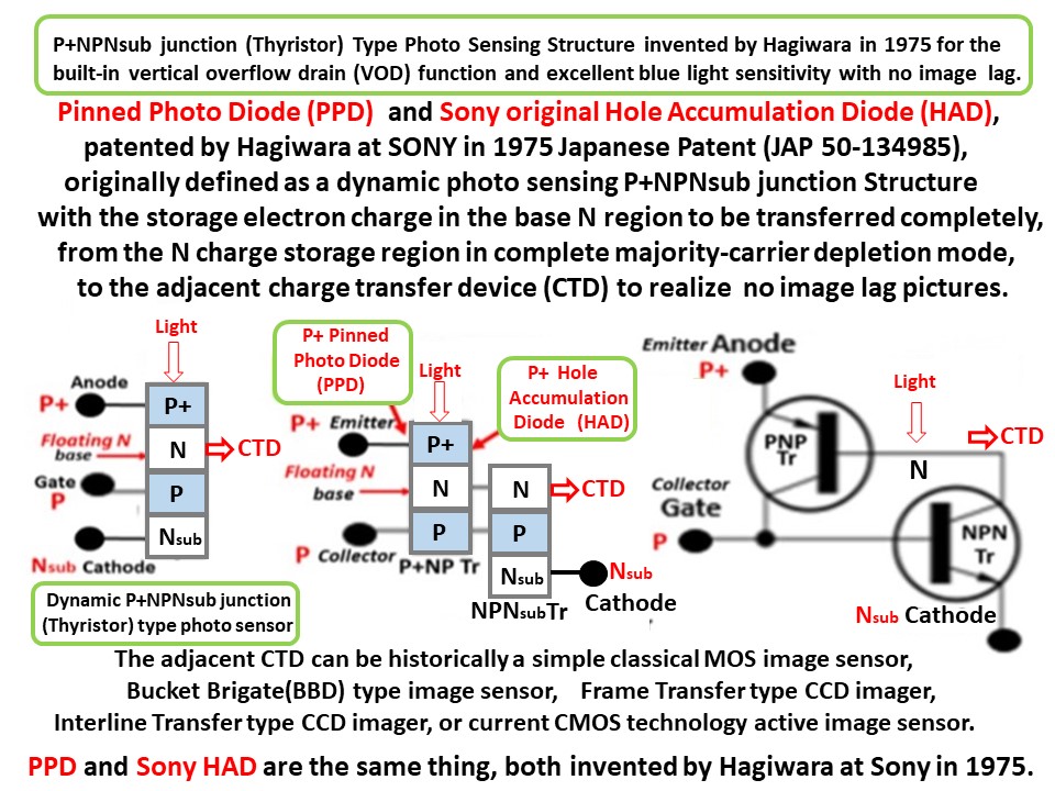
the Pinned Photo Diode. SONY called it as the SONY original HAD sensor.
The truth is that the Pinned Photo Diode and the SONY original HAD sensor
are the same thing, that Hagiwara of SONY invented in 1975.
In conclusion, Hagiwara of SONY invented and his team of many dilligent
and hard working SONY engineers developed the stitching technology
for large area image sensors. The world followed after SONY efforts.
(3) Now, the complete CMOS transistor process scale down was achieved.
And the scale-downed three transistor active source follower type circuits,
originally invented by Peter Noble, can be now easily incorporated in each
picture cell of the CMOS image sesnors, with the help of the P+NP junctiion
type photo diode with the back light illumination scheme, which is again
the
invention by Hagiwara in 1975. See JAP( 1975-127647 ).
SONY diligent and hard working engineers developed the modern dgital
CMOS image sensor with the back light illumination scheme for the
first time in the world.
Now again SONY owns the world record in low-noise in the voltage domain
for the modern digital CMOS image sensors (CISs).
Hagiwara 1975 invention ( JAP 1975-134985 ) helped CCD image sensor in
the past.
Hagiwara 1975 invention ( JAP 1975-127647 ) is helping CMOS image sensor
now.
Hagiwara and his original team of SONY diligent and hard working engineers developed
the stitching technology of both CCD and CMOS large area image sensors.
CCD was considered as the Super Star in the image sensor world in the past,
and the inventors were awarded with the NOBEL prize. But now CCD has
completely dissappeared from the modern digital image sensor world.
So who were the real super stars in the world ?
And now who are the real super stars in the world ?
*******************************************************************
Dear Friends, July 28, 2018
Hi, my name is Yoshiaki Hagiwara, an ex-Sony man.
I worked at Sony from 1975 until 2008.
I was also a visiting professor at CalTech from 1998 t o 1999.
I retired from Sony in 2008.
I was invited in the ISSCC2013 plenary panel.
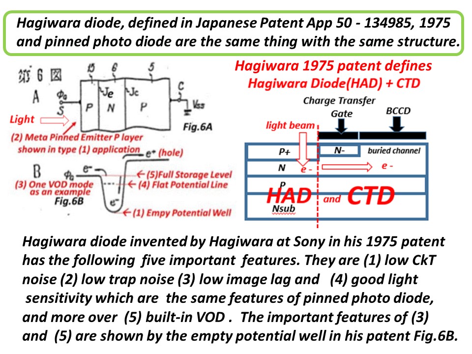
Hagiwara at SONY invented the pinned photo diode in 1975.
See the two Japansese patents below which was filed by Hagiwara in 1975.

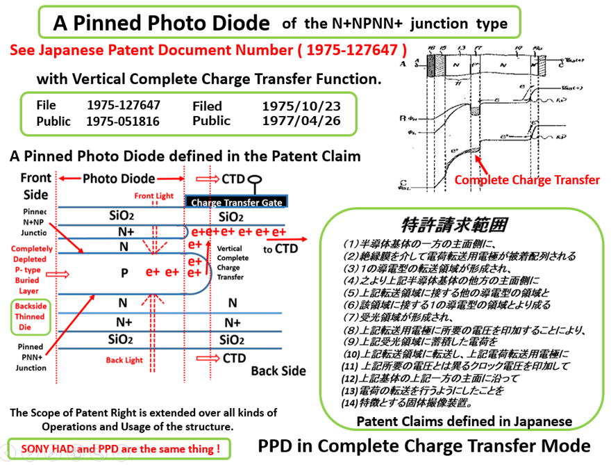
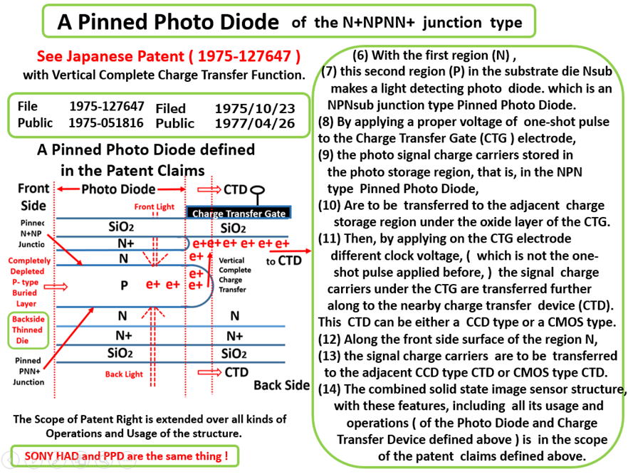
As you can see clearly in the Fig. 7 above, the N+NPN junction type Pinned
Photo
Diode can be operated in the Complete Charge Transfer Mode.
This important Complete Charge Transfer Mode Opertaion is also shown in the
Fig.6B of the PNP junction type Pinned Photo Diode Application shown below.
I believe Hagiwara myself invented the Pinned Photo Diode.
I believe Teranishi did not invent the Pinned Photo Diode.
*******************************************************************
Questions by Prof. Albert Theuwissen are ,
- who invented and developed the stitching technology
for large area image sensors ?
- who owns the world record in low-noise
in the voltage domain for CMOS Image Sensor (CIS) ?
*******************************************************************
Hagiwara believes that
Hagiwara invented it , in the Japanese 1975 patent ( 1975-134985 ) as the P+NPNsub
junction ( Thyristor ) type Light Detecting Picture Cell Structure, and Sony diligent
engineers, including Haggiwara, developed, the stitching technology for large area image
sensors. SONY called it as the SONY original HAD sensor technology in SONY business.
Naturally, the technical world did not use the SONY businesss Brand Name HAD, and
called it by another name, the Pinned Photo Diode. But the Pinned Photo Diode and
SONY original HAD are the same thing, both invented by Hagiwara in 1975.
At least, Teranishi did not invent the Pinned Photo Diode.
Hagiwara is the inventor of the Pinned Photo Diode.
Sony diligent engineers developed and now Sony owns
the world record in low-noise in the voltage domain for CMOS Image Sensor
(CIS)
with the Pinned Photo Diode with the Back Light Illumination, that was
also invented
by Haiwara of SONY in 1975 the Japanses 1975 patent ( 1975-127647 ).
At least, Fossum is not the inventor of the active image sensor picture
element.
Peter Noble is the inventor of the active image sensor picture element.
http://www.pjwn.co.uk/
In the Fossum 2014 fake paper, Fossum attacked Hagiwara 1975 patent with lies,
insulting Sony and Hagiwara honor and pride on purpose. I could not understand
Fossum motivation. But I am now convinced that Fossum wanted Fossum himself
to be recognized by the world, with false explanations on Fossum friend Teranishi
as the TRUE inventor of the Pinned Photo Diode,NOT Hagiwara.
Fossum wanted to convince the world that Fossum himself developed the modern
CMOS digital camera. But now I understand that Peter and SONY diligent engineers
including Hagiwara. This is not fair at all. It is all lies. The world should know the truth.
Until last June I did not know what is the Pinned Photo Diode. I knew SONY HAD.
But I did not know myself that SONY HAD and the Pinned Photo Diode are the
same thing. My friends in Sony informed me that Teranish received awards from
Queen Elizabeth and Japanese Emperor as the inventor of the Pinned Photo Diode.
SONY diligent engineers were not happy at all. Maybe, Albert and Peter also felt it
as a bad news ? So I began to study what is Pinned Photo Diode last June.
Then I found the Fossum 2014 fake paper. I became really MAD at Fossum.
Besides, SONY won the SONY-NEC Patent war by Hagiwara 1975 patent
against the Teranishi1979 patent a long time ago. So Teranish should know that
Hagiwara is the inventor even though Teranishi published his work in IEDM1982.
Teranishi work was just a copy of Hagiwara 1975 patents that defined as one
Example case of Interline CCD image sensor with the complete charge transfer
Mode ( no image lag ) P+NPNsub junction type photon detector structure,
which is now called as the Pinned Photo diode.
But it is now more than four years after Fossum 2014 fake paper publication.
I found this fake paper, really too late.
I was very, very late since I do not belong to the image sensor community any more.
Yes, with my interests in the intelligent image sensors included, but my current major
interests are in the AIP ( Artificial Intelligent Partner ) systems, including AI software
and AI digital circuit system applications.
Yes, I try to be calm, but cannot be silent.
I feel that the world should know at least what is the truth.
I don’t think I can change the past history.
But people can learn the truth anytime, now and in future.
Yes, many people contributed.
Their diligence and efforts must be much worth recognitions.
*******************************************************************
http://www.aiplab.com/Hagiwara_at_Sony_is_the_true_inventor_of_Pinned_Photo_Diode.html
http://www.aiplab.com/Story_of_Pinned_Photo_Diode.html
http://www.aiplab.com/
*******************************************************************
*******************************************************************
**************************************************************************
Evidence that Hagiwara at Sony is the true inventor of the Pinned Photo Diode
**************************************************************************
Evidence that Hagiwara at Sony is the true inventor of the Pinned Photo Diode
is given by the two Japanese patents Hagiwara filed in 1975 at Sony. They are,
Japanese Patent (1975-127647) and (1975-134985). The evidence is described in
details in these two Hagiwara 1975 Japanese patents.
In 1978 Sony announced a new video camera in Tokyo and New York Press
Conferences at the same date, held by Sony Chairman Akio Morita in New York
and Sony President Kazuo Iwama in Tokyo at the same date in 1978.
The video camera was built with the Frame Transfer CCD image sensor
with the Hagiwara invented Pinned Photo Diode light detecting photo sensing
picture cell structure which has a very high light sensitivity, a very low noise
and a very low image lag features.
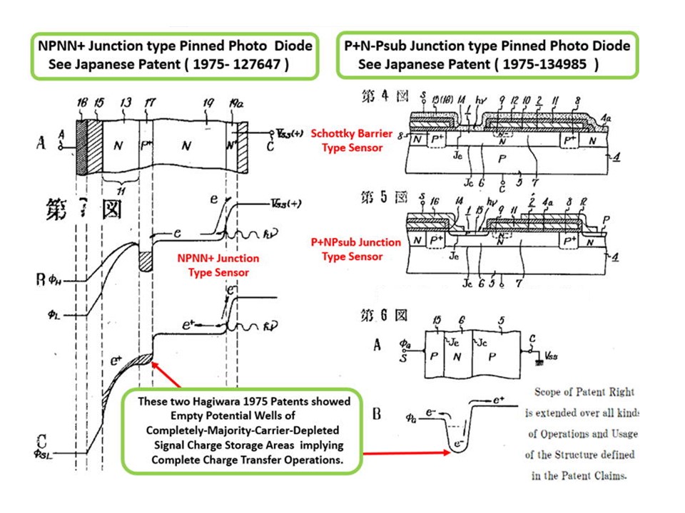
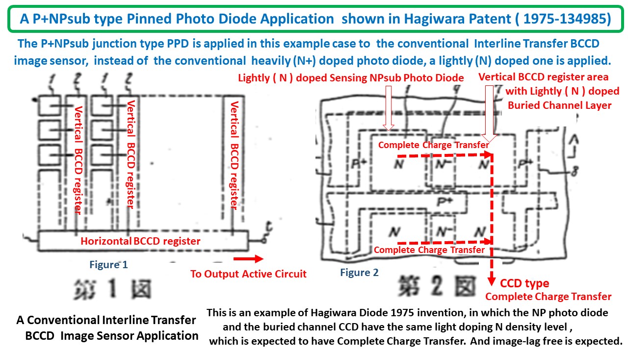
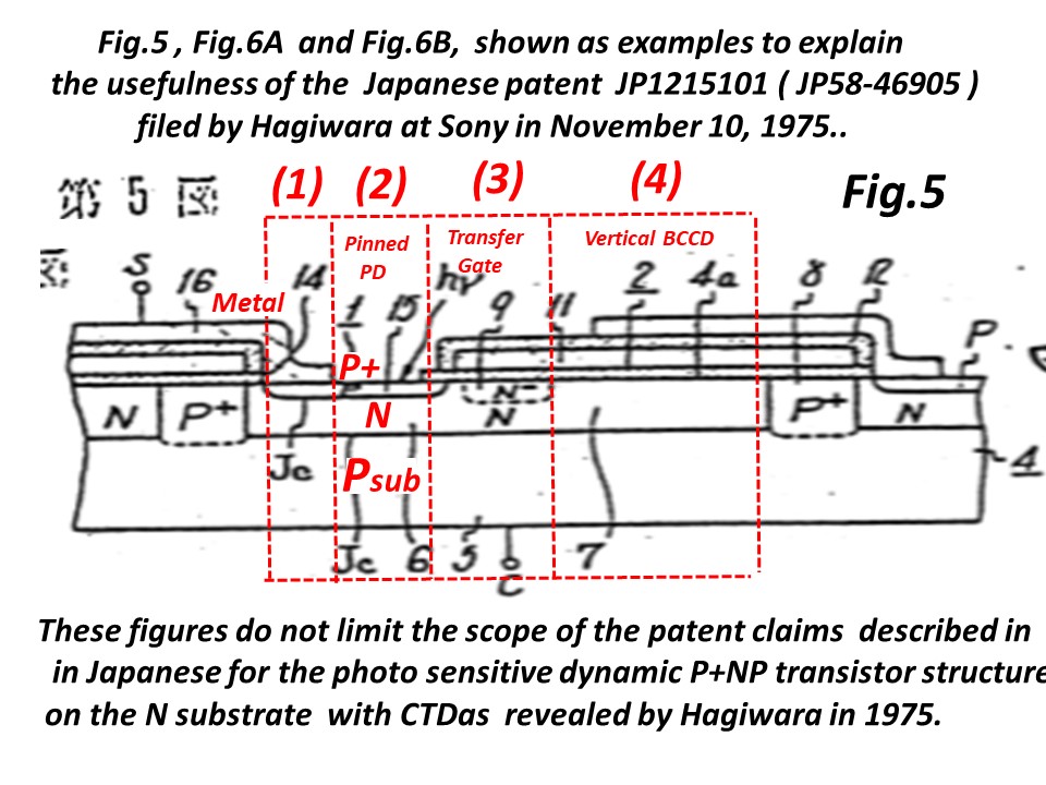
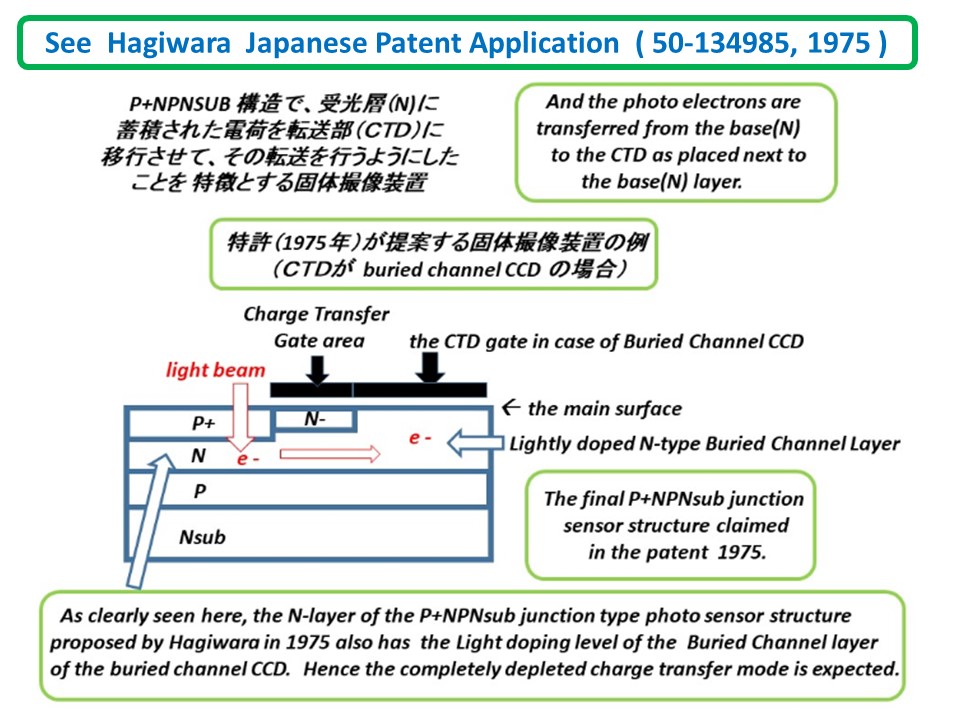
The figures N0.1 thru No.5 in Hagiwara Japanese patent (1975-134985)
explained in details an example of the interline transfer CCD image
sensor application with the Hagiwara invented Pinned Photo Diode.
Sony engineers, after the 1978 Press Conferences in Tokyo and New
York, worked hard for, and succeeded to acquire, the production
and the reliability technolgy of the CCD video camera of the interline
transfer CCD image sensor application with the Pinned Photo Diode
light detecting picture cell structure with the vertical overflow function.
With the diligent SONY engineers efforts, SONY could produce the
portable Passport size Compact CCD image sensor video camera, with
the Pinned Photo Diode that Hagiwara invented in 1975.
And at the same time, Sony filed a trading name officially, which
is the SONY Brand Name of " Sony original HAD sensor " .
With the help of the Hagiwara invented Pinned Photo Diode, which
was now called as " Sony original HAD sensor " with the strong
SONY original sales features of high light sensitivity, low noise and
no image lag characteristics, Sony could become soon very dominant
and strong over the world consumer video camera markets.
The feature of no image lag characteristics in the Hagiwara invented
Pinned Photo Diode is explained and shown in details, as an example
application case, in the figure No.6 of Hagiwara 1975 Japanese Patent
( 1975-134985 ) and also in the figure No.7 of Hagiwara 1975 Japanese
Patent ( 1975-127647 ) in details.
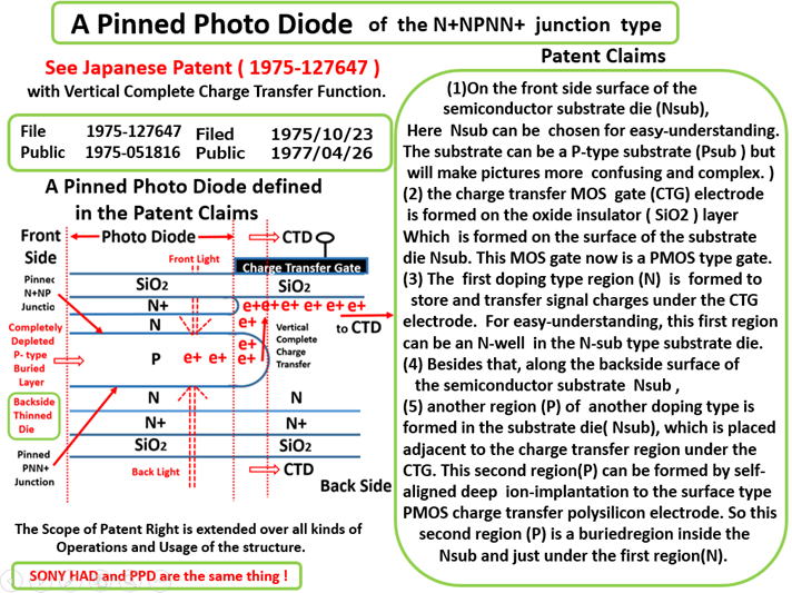
Hagiwara 1975 Japanese Patent ( 1975-127647 ) proposed a Back Light
illumiantion type light detecting photo sensing picture cell structure
with the buried layer type photo signal charge storage. And in the
figure No.7 of Hagiwara 1975 Japanese Patent ( 1975-127647 ) was
shown clearly how the signal charge in the buried storage layer are
trasfered completely to the region under the charge transfer gate
formed on the front side of the silicon wafer. This means clearly
the light sensing picture cell structure, which is now worldly called
as the Pinned Photo Diode, has the very important feature of no
image lag characteristics.
All of these Patent Claim descriptions and Patent figures for possible
patent application examples given in details in the two Hagiwara 1975
Japanese Patents ( 1975-127647 ) and ( 1975-134985 ) support the fact
that Hagiwara is the true inventor of the Pinned Photo Diode.
In conclusion, it is a clear cool fact that Hagiwara at Sony is the true
inventor of the Pinned Photo Diode. The Haiwara patents claims that
the light detecting picture cell structure ( now called as the Pinned
Photo Diode ) can be applied to any kind of charge transfer device(CTD)
which includes the BBD type, the classical MOS type, the CCD type and
the modern CMOS image sensor type charge transfer devices.
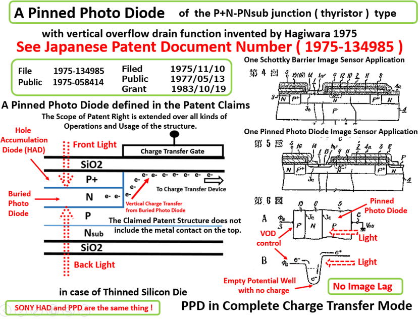
Hagiwara proposed the Pinned Photo Diode with the P+NPNsub junction
(thyrisor) type Light detecting picture cell structure with the vertical
over flow drain for the first time in the world.
Moreoever, Hagiwara proposed in the Japanese patent application example
of figure No.7 of Japanse patent (1975-126747) the Back Light illumination
Pinned Photo Diode type Light Detecting Picture Cell Structure for the
first time in the world.
Moreoever, Hagiwara proposed in the Japanese patent application example
of figure No.4 of Japanse patent (1975-134985) the Schottky Barrier type
Light Detecting Picture Cell structure in the Interline transfer type
CCD image sensor applicaiton for the first time in the world.
**************************************************************************
However last year Hagiwara learned a very surprising news:
**************************************************************
2017 Queen Elizabeth Prize for Engineering Foundation.
**************************************************************
The winners of the 2017 Queen Elizabeth Prize for Engineering Foundation
were :
(1) George E. Smith for the CCD image sensor invention
(2) Michael Tompsett for the CCD image sensor development.
(3) Nobukazu Teranishi for the invention of the pinned photodiode (PPD)
and
(4) Eric Fossum for developing the CMOS image sensor.
**************************************************************
Hagiwara, the true inventor of the Pinned Photo Diode, got really
surprized at the announcement that Teranishi was awarded for the
invention of the pinned photodiode(PPD), and many SONY dilligent
engineers working for the compact digital CMOS image sensors
got really surprized at the announcement that Fossum was awarded
for developing the CMOS image sensor. The truth is that Teranish
did not invent the PPD. Teranish only developped in 1982 the image
lag free interline CCD image sensor with the PPD light detecting
photo sensor structure that was invented by Hagiwara in 1975.
Hagiwara 1975 patents clearly defined the image lag free interline
transfer CCD image sensor as an application example of his 1975
patent claims.
Fossum wrote a paper on "Active Pixel Sensors: Are CCD's
dinosaurs ?" , in Proc. SPIE, Vol.1900, pp.2-14, 1993. However,
the three transistor type active circuit was already invented by
Bill Regitz of Honeywell in 1969. This active pixel sensors was
not Fossum invention. Fossum actually did not develop the
active pixel sensors either. Sony dilligent engineerings did.
Fossum is not the inventor of the active image sensor picture element
at all.
Peter Noble is the true inventor of the active image sensor picture element.
http://www.pjwn.co.uk/
Hitachi MOS Image Sensor Engineers and Intel MOS Process
Engineers all knew that eventually scaled down MOS Process
Technology will conquer all other kinds of Process Technologies
including CCD image sensor technology because of the power
consideration and scaled down dimensional advantage of CMOS
process technology. The three transistor CMOS active picture
cell was already invented as, since the three-transistor circuit
is identical to, the three-transitor circuit of the DRAM cell with
the active source follower type current amplification. Fossum
was just a commentator in his SPIE 1993 paper above. Fossum
was just emphasizing the well understood fact and speculations
that the original image sensor experts all knew in 1970s. This
active pixel sensors was not Fossum invention.Fossum actually
did not develop the active pixel sensors either.
Sony dilligent engineerings developped the active pixel Pinned
Photo Diode type Light detecting photo sensors for compact
digital CMOS image sensors with the Back Light Illumination.
**************************************************************
From these patents it is clear that Hagiwara is the inventor of Pinned
Photo Diode.
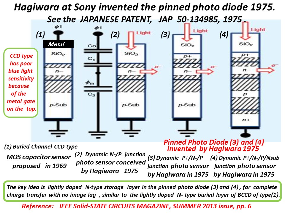
Hagiwara showed that the CCD unique feature of Complete Charge Transfer
Mode
was not unique at all. The pinned photo diode (PPD) invented by Hagiwara
also
have this very important feature of Complete Charge Transfer Mode. Besides,
the PPD invented by Hagiwara has much better light sensitivity because
the
top layer of the PPD sensor area is exposed and covered with the SiO2 glass
like layer . And light can freely pass thru the SiO2 glass like layer.
This is
much better than CCD sensors which have poor light sensitivity due to the
metal electrodes on the top layer in CCD sensors that do not let light
pass thru.
The world does not know the empty potential well
that Hagiwara drew for the first time in the world
in the PNP junction type photo sensor structure (Hagiwara Diode)
that is now also known as pinned photo diode.
The empty potential well is shown below in Fig.6B of Hagiwara 1975 Patent.
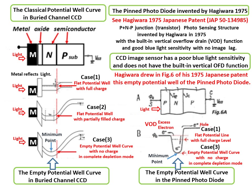
The empty potential well is the result of
the complete charge transfer of the photo electrons
to the adjacent CTD , which implies no image lag high quality pictures.
CTD ( charge transfer device ) described in Hagiwara 1975 patent
can be a CCD type CTD and also a CMOS type CTD.
Hence Hagiwara is the true inventor of the pinned photo diode
which can be applied for both CCD image sensors and CMOS image sensors.
From the evidence shown above, it is clear that Hagiwara at SONY invented
the pinned photo diode in 1975. See the two Japansese patents above
which was filed by Hagiwara in 1975. However, I am now not very happy.
The reason is explained below in details.......
***********************************************************************
Recently I learned about the winners of
2017 Queen Elizabeth Prize for Engineering Foundation.
***********************************************************************
The winners of the 2017 Queen Elizabeth Prize for Engineering Foundation were :
(1) George E. Smith for the CCD image sensor invention
(2) Michael Tompsett for the CCD image sensor development.
(3) Nobukazu Teranishi for the invention of the pinned photodiode (PPD) and
(4) Eric Fossum for developing the CMOS image sensor.
***********************************************************************
I was surprised that Teranishi and Fossum are the two of the four winners.
I don't think that Teranishi invented the pinned photo diode in 1983.
Hagiwara at Sony invented the pinned photo diode in 1975 in his Japansese patent.
I don't think Fossum developped the modern CMOS image sensor.
I think the diligent and silent hard working SONY young engineers developed
the modern CMOS digital image sensor with the Back Light illumination.
Fossum did not invent the three transistor active circuits. The active
circuit
was invented by Rigitz of Honeywell in 1969 and was applied in the Intel
1101
DRAM chip of the three transistor formation of the active source follower
circuits.
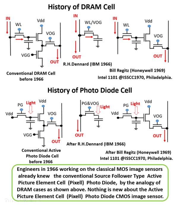
Fossum did NOT invent the active source follower circuit.
Bill Regitz of Honeywell invented it in 1969 as shown above.
Fossum did NOT develop the CMOS digital image sensor at all.
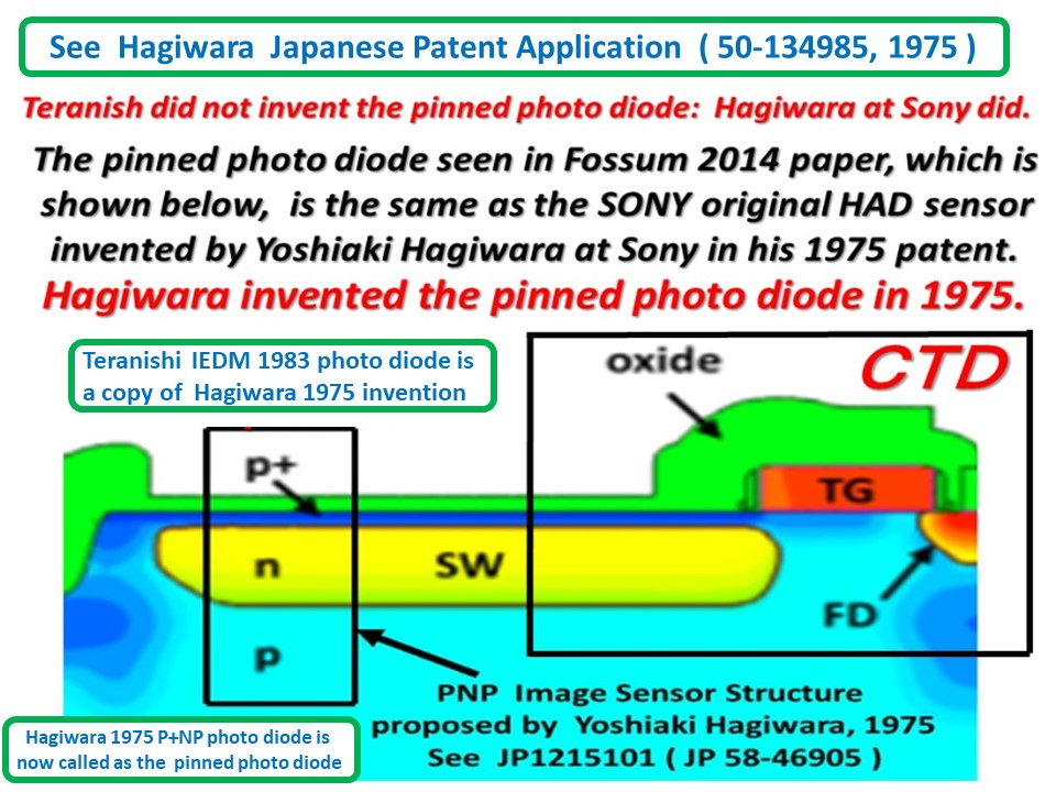
Teranish did NOT invent the Pinned Photo Diode, either.
.
The Teranishi 1983 paper on NEC buried photo diode ILT CCD imager is
the same device that Hagiwara defined in Hagiwara 1975 Japanese patent.
I don't think that Fossum developped the CMOS image sensor alone.
Fossum is not the main contributor of developping the digital CMOS image
sensor.
The digital CMOS image sensor is a product achieved by many people's hard
works
including CalTech Pain's work ( IEDM1998 paper ) on the Snap-shot CMOS
image sensor
and Sony hard working engineers efforts, and still inside with Sony original
HAD sensor,
which is Hagiwara 1975 invention, also now called as the pinned photo diode.
Hagiwara 1975 patent defined the Hagiwara photo diode with a CTD next to
it.
Since CTD includes the classic MOS type CTD, the CCD type CTD and also
the modern dgital CMOS type CTD, Hagiwara is the original inventor of the
modern
digital CMOS type CTD" that includes Sony original HAD digital CMOS
image sensor .
Therefor, I don't think that Fossum developped the CMOS image sensor alone.
Fossum is not the main contributor of developping the digital CMOS image
sensor.
I am the true inventor of the pinned photo diode,
which was defined in my 1975 Japanese patent.
Specially, I am not happy about the fact that the world does not know that
Yoshiaki Hagiwara at Sony actully filed a Japanese patent in 1975 that
defined the pinned photo diode. The problem was that the Hagiwara
patent was written in Japanese, and it is so old that the patent is not
known widely in the world.
Can you judge that the Hagiwara photo sensor structure defined in
Hagiwara 1975 Japanese patent is the pinned photo diode itself ?
I need to hear your point of view on this matter very urgently.
kind regards
Yoshiaki Hagiwara
**********************************************************************
The winners of the 2017 Queen Elizabeth Prize for Engineering Foundation
were :
(1) George E. Smith for the CCD image sensor invention
(2) Michael Tompsett for the CCD image sensor development.
(3) Nobukazu Teranishi for the invention of the pinned photodiode (PPD)
and
(4) Eric Fossum for developing the CMOS image sensor.
***********************************************************************
Fossum is a big liar writing a fake 2014 paper insulting SONY and Hagiwara.
Fossum wrote the fake paper to make the world believe that
Fossum himself was the most important contibutor for realizing
the modern digital CMOS image sensor, which is NOT TRUE.
Many dilligent coworkers with Hagiwara at Sony did the work.
The Sony original HAD sensor, which is also known as the pinned
photo diode and Hagiwara 1975 invention, is still needed to make
the moden digital CMOS image sensor highly light sensitive of
excellent action picture quality of low noise and low image lag.
Fossum 2014 fake paper also made many false and biased statements,
attacking Hagiwara 1975 patent, insulting Hagiwara and SONY original
HAD image sensor which is also known as the pinned photo diode.
Both Sony original HAD sensor and the pinned photo diode sensor are
the same thing that was invented by Yoshiaki Hagiwara at SONY in 1975.
Yoshiaki Hagiwara at SONY is the true inventor of the pinned photo diode.
In Hagiwara's personal opinion, Nobukazu Teranishi and Eric Fossum do
not
deserve the 2017 Queen Elizabeth Prize for Engineering Foundation.
***********************************************************************
Yoshiaki Hagiwara is the true inventor of the pinned photo diode and original digital camera.
The world does not know the truth ( See Hagiwara 1975 patent ).
(1) Teranishi is not the inventor of the pinned photo diode.
(2) Fossum is a big liar writing a fake 2014 paper insulting SONY and Hagiwara.
Fossum is not the true inventor nor the true developper
of the modern digital CMOS image sensor.
Many dilligent coworkers with Hagiwara at Sony did the work.
MOS image sensor was older than CCD image sensor.
Pain and his team in CalTech made a break-thru
for the modern digital CMOS image sensor.
Fossum, using CalTech technology, formed his own company with CalTech
IPs.
Sony teams including Hagiwara did the works
as the true inventor and the true developpers.
Yoshiaki Hagiwara, a Caltech graduate, is the true inventor of the pinned
photo diode and original digital camera.
**********************************************************************
Important Contributions for Image Sensor Developmet Efforts before 1975
**********************************************************************
J.Bardeen and W.H.Brattain, "Transistor: A Semiconductor Triode",
Physical Review, VOl.74, p.230, July 1948.
W.Shockley, "The theory of p-n Junction in Semiconductor and p-n
Junction Transistor", Proc. IEEE Vol.51, pp.1190-1202, September 1949.
S.R.Hofstein and F.P.Heiman, "The Siliocn Insulated-Gate Field Effect
Transistor", Proc. IEEE Vol.51, pp.435-1202, September 1963
Gordon E. Moore, "Cramming more components onto integrated circits",
Electronics,
Vol.38, No.8, April 19, 1965.
M.A.Schuster and G.Strull, " A Monolithic Mosaic of Photo Sensors for Solid
State Imaging Application", IEEE Trans. Electron Devices, Vol.ED-13, No.12, 1966
A. S. Grove, “Physics and Technology of Semiconductor Devices,”
John Wiley and Sons, Inc., New York pp.136-140, no.267, 1967.
P.K.Wiener, et al "A self-Scanned Solid State Image Sensor", in Proc. IEEE,
Vol 55, No.9, 1967.
G.P.Weckler, "Operation of PN Junction Photo Detectors in a Photon Flux
Integrating Mode", IEEE J. Solid State Circuits. Vol2, pp.65-73, September 1967.
P.J.W. Noble, "Self-Scanned Silicon Image Dector Arrys", IEEE Trans. Electron
Devices, Vil.ED-15, No.4, pp.202-209,1968.
S.G. Chamberlain, "Photosensitivity and Scanning of Silicon Image Detector
Arrays" IEEE J.Solid State Circuits, Vol.SC-4, No.6, pp.333-342, 1969.
F.L.J.Sangster and K.Teer, "Bucket Brigate Electronics - New Possibilities
for Delay Time-Axis Conversion and Scanning", IEEE J.Solid-State Circuits,
VOl.SC-4, No.3, pp.131-136, 1969.
W. S. Boyle and G. E. Smith, “Charge-Coupled Semiconductor Devices,”
Bell Syst. Tech. J., 49, pp.587-593, 1970.
W.M.Regitz and J.Karp, "A Three-transistor-cell, 1024 bit, 500 nsec
MOS RAM", ISSCC1970, Feb. 1970
F.L.J. Sanger, "Integrated MOS and Bipolar Analog Delay Lines using
Bucket Brigate Capacitor Storage", ISSCC1970, pp.74-75, 185, Feb. 1970.
G.F.Amelio, M.F.Tompsett and G.E.Smith, "Experimantal Verification of the
Charge Coupled Semiconductor Devices", B.S.T.J.Vol.49,pp.587-593,Apr. 1970
W.M.Regitz and J.Karp, "A Three-transistor-cell, 1024 bit, 500 nsec
MOS RAM", IEEE JSSC, VOl.SC-5, No.5, pp.181-186, October 1970.
W.F.Kosonocky and J.G.Carns, " Charge Coupled Digital Circuits", ISSCC1971,
pp.161-163, February 1971
G. F. Amelio, W. J. Bertram, Jr., and M. F. Tompsett,
“Charge-Coupled Imaging Devices: Design Considera- tions,”
IEEE Trans. Electron Devices, ED-18, no.11, pp.986-992, 1971.
M.F.Tompsett, et al "Charge Coupled Imaging Devces Experimental Results",
IEEE Trans. Electron Devices, Vol. ED-18, No.11, pp.992-996, 1971.
J.E.Carnes, "Drift-Aiding Fringing Fields in Charge Coupled Devices", IEEE J.
Solid State Circuits, Vol.SC-6, No.5, pp.322-326, 1971.
W.F.Kosonocky and J.G.Carns, " Charge Coupled Devices" ISSCC1972,
pp.132-133, February 1972.
C.H.Sequin, "Blooming Supression in Charge Coupled Area Imaging" Bell Sys.
Tech. J., 51, oo. 1923-1926, 1972.
J.D.Plummer and J.D.Meindl, " A Low-Light-Level Self-Scanned MOS Image
Sensor" ISSCC1972 Dig.Tech.Paper pp.30-31, February 1972.
J. E. Carnes and W. F. Kosonocky,
“First Interface-State Losses in Charge-Coupled Devices,”
Appl. Phys. Lett., vol.20, pp.261-263, 1972.
J. E. Carnes and W. F. Kosonocky,
“Noise Sources in Charge-Coupled Devices,”
RCA Review, vol.33, pp.327-343, 1972.
R. H. Walden, R. H. Krambeck, R. J. Strain, J. McKenna,
N. L. Schryer, and G. E. Smith, “The Buried Channel Charge
Coupled Devices,” Bell Syst. Tech. J., no.51, pp.1635-1640, 1972.
G. F. Amelio, “Physics and Applications of Charge Coupled Devices,”
IEEE INTERCON, New York, Digest, vol.6, paper 1/3, 1973.
D. M. Erb, W. Kotyczka, S. C. Su, C. Wang, and G. Clough,
“An Overlapping Electrode Buried Channel CCD,”
IEDM, Washington, D.C., Tech. Digest, pp.24-26, 1973.
W. F. Kosonocky and J. E. Carnes,
“Two Phase Charge Coupled Devices with Overlapping Polysilicon
and Aluminum Gates,” RCA Review, vol.34, pp.164-202, 1973.
D.M.Erb,W.Kotyczka, S.C. Su, C.Wamg and G.Clough, "An Overlapped
Electrode Buried Channel CCD", IEDM1973, Dec 3-5, 1973.
S. R. Shortes et al., “Development of a thinned backsideilluminated
charge-coupled device image,” in Proc. IEDM1973, Dec. 1973, p. 415.
N.G. Vogi, et al "A Half-Million Pel Bucket Brigate Optical Scanner",
ISSCC1974, pp. 30-31, February 1974.
P. A. Gray and H. Coltman, “Back surface imaging of thinned CCDs,”
in Proc. CCD, 1974, pp. 162?167.
J. Lohstroh, "The JFET as a Photosensitive Cell in Image Sensor Arrys",
ISSCC1974, pp. 34-35, February 1974.
M.H. White, "Characterization of Surface CHannel CCD Image Arrays at
Low Light Level", IEEE J. Solid State Circuits, Vol.SC-9, No.1, pp.1-12, 1974.
A. W. Lees and W. D. Ryan, “A Simple Model of a Buried-Channel
Charge-Coupled Device,” Solid-State Electron., vol.17, pp.1163-1169, 1974.
C. H. Sequin, F. J. Morris, T.A. Shankoff, M. F. Tompsett, and E. J. Zimany,
“Charge-Coupled Area Image Sensor Using Three Levels of Polysilicon,”
IEEE Trans. Electron Devices, ED-21, pp.712-720, 1974.
M. H. White, D. R. Lampe, F. C. Blaha, and I. A. Mack,
“Characterization of Surface Channel CCD Imaging Arrays
at Low Light Levels,” IEEE Trans. Solid-State Circuits,
SC-9, pp.1-13, Feb. 1974.
D. F. Barbe, “Imaging Devices Using the Charge-Coupled Concept,”
Proc. IEEE, vol.63, no.1, pp.38-67, 1975.
C. H. Sequin and M. F. Tompsett, “Charge Transfer Devices,”
Academic, New York, 1975.
James M. Early ( Fairchild Camera and Instrument Corporation, USA ) "Charge
Coupled Device with Overflow Protection", USP 3896485, July 22, 1975.
Hagiwara
had to protect his 1975 Japanese patent ( 1975-127647 ) on the P+NPNsub
Junction (Thyristor ) type Light Detecting Picture Cell Structure agaist
this
Fairchild Early USP 3896485 patent. The SONY-Fairchild Patent War lasted
from
1991 till 2000. Finally, Sony won the Patent war over Fairchild. But during the
long period of 10 years, Hagiwara felt as if he was in Jail and could not
perform
any important job tasks in Sony at all.
*************************************************************
Hagiwara Contributions for Image Sensor Developmet Efforts
*************************************************************
Hagiwara ISSCC1974 Paper on "Buried Channel CCD Charge Transfer"
February 1974 in Philadelphia, USA. This was Hagiwara PhD thesis paper
at California Institute of Technology (CalTech) Pasadena, California USA>
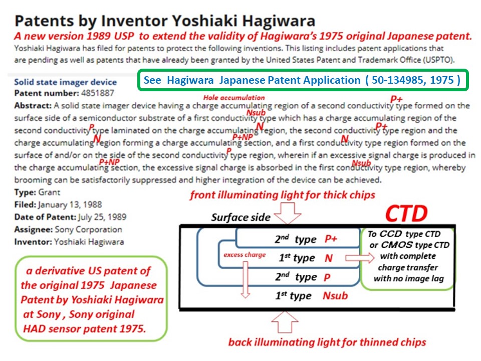
Hagiwara, 1975 Japanese Patent ( JA 1975-127647 ) at SONY
on the Pinned Photo Diode with Back Light Illumination
Hagiwara, 1975 Japanese Patent ( JA 1975-134985 ) at SONY
on the Pinned Phodo Diode with Vertical Overflow Drain Function
C.A.Mead, R.D.Pashley,Lee D. Britton, Yoshiaki T.Daimon Hagiwara and
S.F. Sando, "128-Bit Multicomparator", J. Solid State Circuits, Vol.SC-11,
No.5, October 1976. This is important for intelligent image sensor systems.
Hagiwara, 1978 Solid State Semiconductor Device Conference Paper on
"Narrow Channel Frame Transfer CCD Image Sensor" at Tokyo, Japan .
This is the first paper in the world reporting the P+NP type ( dynamic
PNP junction ( photo transistor ) type light detecting picture element
structure, which was later called as the Pinned Photo Diode.
Y. Daimon-Hagiwara, M. Abe, and C. Okada, “A 380Hx488V CCD imager
with narrow channel transfer gates,” Japanese J. Appl. Phys., vol. 18,
supplement 18?1, pp. 335?340, 1979.
Hagiwara, CCD'79 invited paper on "SONY Image Sensor Efforts"
at Edinburgh, Scotland UK on SONY CCD image sensors.
Fumio Miyaji, Yasushi Matsuyama, Yoshikazu Kanaishi, Katsunori Senoh,
Takashi Emori and Yoshiaki Hagiwara, "A 25 nanosec 4 Mega bit CMOS
RAM with DYnamic Bot-Line Loads", ISSCC1989 and J.Solid State Circuits,
Vol24, No.5, October 1989. This wad for Cache SRAM memory for SONY
Compact Digital CCD Image Sensors.
Y. Hagiwara, “High-density and high-quality frame transfer CCD imager
with very low smear, low dark current and very high blue sensitivity,”
IEEE Trans. Electron Devices, vol. 43, no. 12, pp. 2122?2130, Dec. 1996.
Hagiwara, ESSCIRC2001 invited paper on "SONY Consumer Electronics"
at Vilach, Austria
Hagiwara, ESSCIRC2008 invited paper on "SOI Cell Processor and Beyond"
at Edinburgh, Scotland UK
Hagiwara, the 60th Aniversary ISSCC2013 Plenary Panel Talk,
at San Franicisco, USA
***************************************************************************
Important Contributions for Image Sensor Developmet Efforts after 1975 and later.
***************************************************************************
Gilbert F. Amelio ( Fairchild Camera and Instrument Corporation, USA )
"Self Aligned CCD Element including Two Levels of Electrondes and
Method of Manufacture therefor" USP 3931674, Jan 13, 1976.
This Amelio patent (USP3931674) which was judged invalid by the prior
art of USP3745647 by Boleky and by IEDM1973 paper by D.M.Erb,
W.Kotyczka, S.C.Su, C.Wamg and G.Clough, "An Overlapped Electrode
Buried Channel CCD", IEDM1973, Dec 3-5, 1973.
T. Yamada, H. Okano, and N. Suzuki, “The Evaluation of Buried Channel Layer
in BCCD’s,” IEEE Trans. Electron Devices, ED-25, no.5, pp.544-546, 1978.
J. Hynecek, “Virtual phase CCD technology,” in Proc. IEDM1979, pp. 611?614,
Dec. 1979,
J.Nishizawa, et al, "Static Induction Transistor Image Sensors", IEEE Trans.
Electron Devices, Vol.ED-26, No.12, pp.1970-1977, 1979.
A. Furukawa, Y. Matsunaga, N. Suzuki, N. Harada, Y. Endo, Y. Hayashimoto, S. Sato,
Y. Egawa, and O. Yoshida, “An Interline Transfer CCD for A Single Sensor 2/3” Color
Camera,” IEDM, Washington, D. C., Tech. Digest, pp.346-349, 1980.
K.Hoshi, T.Suzuki, Y.Okubo and N.Isawa, "CZ Siliocn Crystal grown in Transverse
Magnetic Fields", 157th ECS Mtg Ext. Abstract, pp.811-813, May 1980.
T.Asada and F.Nagumo, "A New CCD Digital Color Camera using Direct Encoding
Method", Int. Conf. on Digital Signal Processing, September 2-5, 1981, Florence Italy.
Y. Ishihara, E. Oda, H. Tanigawa, N. Teranishi, E. Takeuchi, I. Akiyama, K. Arai,
M. Nishimura, and T. Kamata, “Interline CCD Image Sensor with an Anti Blooming
Structure,” ISSCC Digest of Technical Papers, pp.168-169, Feb. 1982.
N. Teranishi, A. Kohno, Y. Ishihara, E. Oda, and K. Arai, “No Image Lag Photodiode
Structure in the Interline CCD Image Sensor,” IEDM Tech. Dig., pp.324-327, 1982.
Y.Ishihara and K.Tanigaki,"A High Photosensitivity IL-CCD Image Sensor with
Monolithic Resin Lens Array", IEDM1983 Tech. Dig, pp.497-500, December 1983.
B.C. Burkey et al, "The Pinned Photo Diode for an Interline Transfer Image Sensor",
IEDM1984, DIg.Tech.Papers, pp.28-31, December 1984.
K. Horii, T. Kuroda, and S. Matsumoto, “A New Configuration of CCD Imager with a
Very Low Smear Level -FIT-CCD Imager,” IEEE Trans. Electron Devices, ED-31, no.7,
pp.904-909, 1984.
Y. Matsunaga and N. Suzuki, “An Interline Transfer CCD Imager,” ISSCC Digest of
Technical Papers, pp.32-33, Feb. 1984.
M.Ogawa et al, "Signal-PRocesiing ICs employed in a Single-Chip CCD Color Camera",
IEEE TRansaction on Consumer Electronics, Vol.CE-30, No.3, pp.374-381, Aug.1984
T.Kumezawa et al, "High Resolution CCD Image Sensors with Reduced Smear", IEEE
transaction on Electron Devices, VOl. ED-32, No.8, pp.1451-1456,1618, Aug. 1985.
Y.Ogawa et al, "Development of CCD Imaging Block for Single Chip Color Camera",
IEEE Transaction on Consumer Electronics, Vol.CE-31, No.3, pp.405-413, Aug. 1985
T.Nakamura,"A New MOS Image Sensor Operating in a Non-destructive Readout
Mode", IEDM1986, Tech.Dig. pp.353-356, December 1986.
M.Yamamura et al, "A 1/2 inch CCD Imager with 510 x 492 pixels", SPIE Vol.765
Image Sensors and Displays pp.41-46, Jan 13-14, 1987.
T. Yamada, K. Ikeda, and N. Suzuki, “A Line-Address CCD Image Sensor,”
ISSCC Digest of Technical Papers, pp.106-107, Feb. 1987.
T. Yamada, T. Yanai, and T. Kaneko, “2/3 Inch 400,000 Pixel CCD Area Image Sensor,”
Toshiba Review, no.162, pp.16-20, Winter 1987.
N. Teranishi and Y. Ishihara, “Smear Reduction in the Interline CCD Image Sensor,”
IEEE Trans. Electron Devices, ED-34, no.5, pp.1052-1056, 1987.
A.J.P.Theuwissen et al, "A 400K Pixel 1/2 inch Accorion CCD Imager", ISSCC1988,
Dig.Tech.Papers, pp.48-49, February 1988.
M. Hamasaki, T. Suzuki, Y. Kagawa, K. Ishikawa, M. Miyata, and H. Kambe,
“An IT-CCD Imager with Electronically Variable Shutter Speed,” ITEJ Technical
Report, vol.12, no.12, pp.31-36, 1988.
H.Yamashita et al, "A New High Sensitivity Photo-transitor for Area
Image Sensors", IEDM1988 Tech Dig pp.353-356, December 1988.
J.Hynecek, "A New Device Architecture Suitable for High-Resolution
and High Performance Image Sesnors", IEEE Trans, Electron Devices,
Vol.35, No.5, pp.646-652, 1988.
N.Tanaka, et al,"A Novel Bipolar Imaging Device with Self-NOise Reduction
Capability", IEEE Trans. Electron Devices, Vol.36, No.1, pp.31-38, 1989
K.Yonemoto et al, "A 2 million Pixel FIT-CCD Image Sensor for HDTV
Camera System" IEEE ISSCC1990, pp.214-216, February 1990.
F.Andoh et al,"A 250 000 Pixel Image Sensor with FET Amplification
at Each Pixel for High Speed Television Cameras", ISSCC1990, Dig.Tech.Papers
pp.212-213, February 1990.
Eric G. Stevens et al, "A One Mega Pixel Progressive Scan Image Sensor with
Antiblooming Control and Lag-Free Operation", IEEE Trans. Electron Devices,
Vol38, No.5, pp.981-988, 1991.
K.Ishikawa and T.Iizuka, "One inch 2M pixel CCD with Hyper HAD sensor and
Camera System for HDTV", SPIE proc. Vol. 1656, pp.30-40, February 1992.
T. Ishigami, A. Kobayashi, Y. Naito, A. Izumi, T. Hanagata, and K. Nakashima,
“A 1/2-in 380k-pixel Progressive Scan CCD Image Sensor,” ITE Technical Report
Vol.17, no.16, pp.39-44, Mar. 1993.
P.B.Denyer et al, "CMOS Image Sensors for Multimedia Applications", IEEE
Constum Integrated Circuits Conference 1993, Proc. of CICC1993,
pp.11.5.1-11.5.4, 1993.
H.Kawashima et al, "A 1/4 inch Format 250K Pixel Amplified MOS Image Sensor
Using CMOS Process", IEDM1993, Tech. Dig. pp.575-578, December 1993.
S.K.Mendis et al, "128 x 128 CMOS Active Pixel Image Sensor for Highly Integrated
Imaging Systems", IEDM1993, Tech. Dig. pp.583-586, December 1993.
E.R.Fossum,"Active Pixel Sensors: Are CCD's dinosaurs ?" , in Proc. SPIE,
Vol.1900, pp.2-14, 1993.
Hitachi MOS Image Sensor Engineers and Intel MOS Process Engineers all
knew
that eventually scaled down MOS Process Technology will conquer all other
kinds of Process Technologies including CCD image sensor technology because
of the power consideration and scaled down dimensional advantage of CMOS
process technology. The three transistor CMOS active picture cell was already
invented as, since the three-transistor circuit is identical to, the three-transitor
circuit of the DRAM cell with the active source follower type current amplification.
Fossum was just a commentator in his SPIE 1993 paper above, emphasizing
the fact
and speculations that the original image sensor experts and engineers all
knew in 1970s.
R.H.Nixon et al, "128 x 128 CMOS Photodiode Type Active Pixel Sensor
with On-ChipTiming Ccntrol and Signal CHain Electronics", in Proc. SPIE,
Vol.2415, pp.117-123, 1995.
S. Kawai et al, "Photo Response Analysis in CCD Image Sensors with a VOD
Structure", IEEE TRans. Electron Devices, VOl.42, No.4, pp.652-655, 1995.
Paul P. K. Lee et al, "An Active Pixel Sensor Fabricated Using CMOS/CCD
Process Technology", in Proc. IEEE Workshop on CCDs and Advanced
Image Sesnors", 1995.
S.Kawahito et al,"A Compressed Digital Output CMOS Image Sensor with
Analog 2-D DCT Processors and ADC/Quantizer",ISSCC1997, Dig.Tech.Papers,
pp.184-185, February 1997.
T. H. Lee, R. M. Guidash, and P. P. Lee, “Partially pinned photodiode
for solid-state image sensors,” U.S. Patent 5,903,021, Jan. 1997.
R. M. Guidash, “Active pixel image sensor with shared ampli?er
readout,” U.S. Patent no. 6,107,655, Aug. 1997.
Walter F. Kosonocky et al, "360 x 360 Element Three-Phase Very High
Frame Rate Burst Image Sesnor, Design, Operation and Perfomance",
IEEE Trans. Electron Devices, Vol.44, No.10, pp.1617-1624, 1997.
R.M.Guidash et al, "A 0.6 um CMOS Pinned Photo Diode Color Imager
Technology", IEDM1997, Tech. Dig. pp.927-929, December 1997.
M.Loinaz, et al, "A 200mW 3.3V CMOS Color Camera IC Producing
352 x 288 24b Video at 30 Frames/sec", ISSCC1998, Dig.Tech.Papers,
pp.168-169, February 1998.
Guang Yang, Orly Yadid-Pecht, Chris Wrigley, and Bedabrata Pain ,
"A Snap-Shot CMOS Active Pixel Imager for Low-Noise, High-speed
Imaging", IEDM1998, December 1998.
F.Andoh et al, "A Digital Pixel Image Sensor with 1 bit ADC and
8 bit Pulse Counter in Each Pixel", International Image Sensor
Workshop, P1, 1999.
K. Yonemoto et al, "A CMOS Image Sensor with a Simple FPN
Reduction Technology and a Hole Accumulation Diode", ISSCC2000,
Dig.Tech.Papers, pp.102-103, February 2000.
T. Yamada, Katsumi Ikeda, Y. G. Kim, H. Wakoh, T. Toma, T. Sakamoto,
K. Ogawa, E. Okamoto, K. Masukane, K. Oda, and M. Inuiya, “A progressive
Scan CCD Image Sensor for DSC Applications,” IEEE J. of Solid-State
Circuits, vol.35, no.12, pp.2044-2054, 2000.
M.Furuyama et al,"High Sensitivity and No Crosstalk Pixel Technology
for Embedded CMOS Image Sesnor", IEEE Trans. Electron Devices,
Vol.48, No.10, 2001.
T.Miida,"A 1.5 M Pixel Imager with Localized Hole-Modulation Method",
ISSCC2002, Dig.Tech.Papers, pp.42-43, February 2002.
T. GOji Etoh,"A CCD Image Sensor of 1Mframe/sec for Continuous
Image Capturing 103 Frames", ISSCC2002, Dig.Tech.Papers, pp.46-47,
February 2002.
T.Sugiyama et al, "A 1/4 inch QVGA Color Imaging and 3-D Sensing
CMOS Sensor with Analog Frame Memory", ISSCC2002,Dig.Tech.Papers,
pp.434-435, February 2002.
A. Theuwissen, "50 years of Solid State Image Sensors",
ISSCC2003, Dig.Tech. Papers, S26, February 2003.
I. Inoue et al., “Low-leakage-current and Low-operating-voltage
Buried Photodiode for a CMOS imager,” IEEE Trans. Electron Devices,
vol. 50, no. 1, pp. 43?47, Jan. 2003.
K.Mabuchi,N.Nakamura, E.Funatsu,T.Abe,T.Umeda,T.Hoshino,R.Suzuki,
H.Sumi, "CMOS Image Sensor Using a Floating Diffusion Driving Buried
Photo Diode", ISSCC2004, pp.112-113, February 2004.
H.Takahashi et al, "A 3.9 um Pixel Pitch VGA Format, 10 bit Digital
Image Sensor with 1.5 Transistor /Pxcel", ISSCC2004, pp.108-109, Feb. 2004.
M.Mori et al, "A 1/4 inch 2M Pixel CMOS Image Sensor with 1.75
Transistor/Pixel", ISSCC2004, pp.110-111, February 2004.
Nana Akahane, Rie Ryuzaki, Satoru Adachi, Koichi Mizobuchi,
Shigetoshi Sugawa, "A 200dB Dynamic Range Iris-less CMOS Image
Sensor with Lateral OverflowIntegration Capacitor using Hybrid Voltage
and Current Readout Operation", ISSCC2006, pp.300-301, Feb.7, 2006.
Shin Iwabuchi et al,"A Back illunated High Sensitivity Small Pixel
Color CMOS Image Sensor with Flexible Layout of Metal Wiring",
ISSCC2006, pp.302-303, Feb.7, 2006
Y. Nitta et al, "High Speed Digital Double Sampling with Analog CDS
on Column parallel ADC Architecture for Low Noise Active Pixel Sensor",
ISSCC2006, pp.500-501, Feb. 8, 2006
S.Yoshihara et al, "A 1/1.8 inchi 6.4 Mega Pixel 60 frames/sec CMOS
Image Sensor with Seamless Mode Change", ISSCC2006, Dig.Tech.Papers
pp.1984-1993, February 2006.
K.Cho et al, " A 1/2.5 inch 8.1 Mega Pixel CMOS Image Sesnor for
Digital Camera",ISSCC2007, Dig.Tech.papers pp.508-509, February 2007.
S-H Cho et al, "Optoelectronic Investigation for High Performance 1.4 um
pixel CMOS Image Sensors", International Image Sensor Workshop (IISW2007),
June 6-10, 2007.
Xinyang Wang, Padmakumar R.Rao, and Albert J.P. Theuwissen,
"Characterization of the Buried CHannel NMOS Source Followers
in CMOS Image Sesnors", International Image Sensor Workshop
(IISW2007), June 6-10, 2007.
Shoji Kawahito and Nobuhiro Kawai, "Column Parallel Signal
Processing Techniues for Reduing Thermal and RTS Noises in
CMOS Image Sensors", International Image Sensor Workshop
(IISW2007), June 6-10, 2007.
G.Agranov et al, "Super Small Sub 2 um Pixels for Novel CMOS
Image Sensors", International Image Sensor Workshop (IISW2007),
June 6-10, 2007.
J.Prima et al, "A 3 Mega Pixel Back illuminated Image Sensor
in 1T5 Architecture with 1.45 um Pixel Pitch", International
Image Sensor Workshop (IISW2007), June 6-10, 2007.
B.Cremers et al, "A High Speed Pipelined Snapshoto CMOS Image
Sensor with 6.4 Gpixel/sec Data Rate", International Image Sensor
Workshop 5.9, p.9, 2009.
K.Itonaga et al, "Extremely Low Noise CMOS Image Sensor
with High Saturation Capacity", IEDM2011, Dig.Tech.Papers
pp.171-174, December 2011.
M.Sakakibara et al,"An 83 dB Dynamic Range Single Exposure Global
Shutter CMOSImage Sensor with In-Pixek Dual Storage", ISSCC2012,
Dig.Tech.Papers, 22.1, pp.380-381, February 2012.
T.Tochigi et al, "A Global Shutter CMOS Image Sensor with Readout
Speed of One Tpixel/secBurst and 780 Mpixel/sec Continuous",
ISSCC2012, Dig.Tech.Papers, 22.1, pp.382-384, February 2012.
E.R.Fossum and D.B.Hondongwa, " A Review of the Pinned Photo Diode
for CCD and CMOS Image Sensors", IEEE J. of Electron Devices Society,
VOL-2, No.3, May 2014. This is a fake paper which did not quote the
Hagiwara 1975 patent on the Back Light Illuminated Pinned Photo Diode
Light Detecting Element Structure ( 1975-127647 ) with the complete
charge transfer operation mode with the image lag free feature. This
Fossum fake 2014 paper made also many false statements on the Hagiwara
1975 patent on the P+NPNsub junction (thysitor) type Pinned Photo Diode
Light Detecting Element Structure ( 1975-134985 ) that has the complete
charge transfer action with no image lag feature, and also with the built-in
vertical overflow drain (VOD) function.
***********************************************************************
***********************************************************************
return to http://www.aiplab.com
return to http://www.aiplab.com/Story_of_Pinned_Photo_Diode
********************************************************************