*******************************************************************************
Hagiwara at Sony is the true inventor of Pinned Photo Diode
See also Japanese Patent 1975-134985
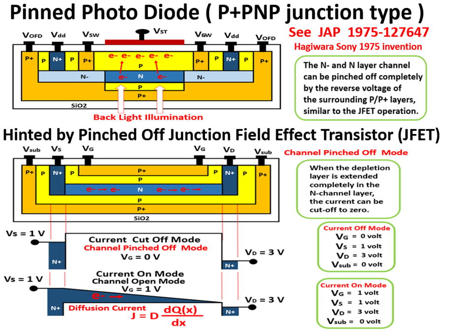
and Japanese Patent 1975-127647
Private Communications with Prof. Albert Theuwissen
******************************************************************************
Hagiwara Yoshiaki, the inventor of Pinned Photodiode
*******************************************************************
Invited talks related to the invention of
Pinned Photodiode ( SONY HAD sensor )
(1) International Conference CCD79 in Edinburgh, Scotland UK
(2) International Conference ESSCIRC2001 in Vilach, Austria.
(3) International Conference ESSCIRC2008 in Edinburgh, Scotland UK
(4) International Conference of Solid State Circuits ISSCC2013
in San Francisco, California, USA , February 2013
******************************************************************
Publication List of Hagiwara Yoshiaki while a PhD student at Caltech.
(1)"The Influence of Interface States on Incomplete Charge
TRansfer in Overlapping Gate Charge-Coupled Devices"
by Amr M.Mohsen, T.C.McGill, Yoshiaki Daimon Hagiwara,
and Carver A. Mead, IEEE Journal of Soild-State Circuits
Vol. SC.8 , No.2, April 1973
(2)"Buried Channel CCD Charge Transfer" by Yoshiaki Hagiwara,
T.C.McGill, and Carver A. Mead, ISSCC1974 Paper
in Philadelphia, USA, February 1974
(3)"Final Stage of the Charge-Transfer Process in Chrge-Coupled
Devices" by Yoshiaki Daimon Hagiwara, Amr M. Mohsen, and
T.C.McGill, IEEE Transactions on Electron Devices, VOl. ED-21,
No.4, April 1974
(4) "128-Bit Mutlicomparator", C.A.Mead, R.D.Pashley, L.D.Brutton,
Yoshiaki Daimon Hagiwara and S.F.Sando, IEEE Journal of
Soild-State Circuits Vol. SC.11 , No.4, October 1976
Publication List of Hagiwara Yoshiaki at Sony
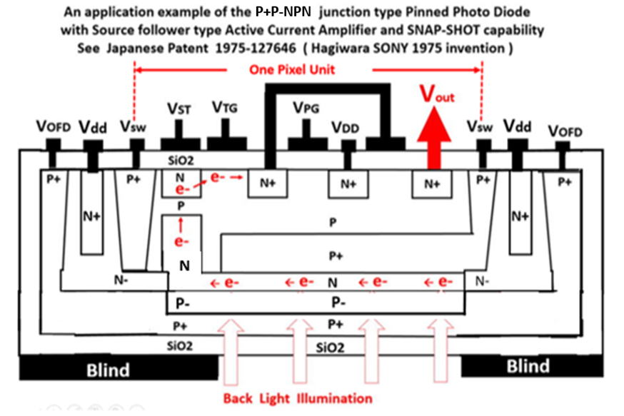
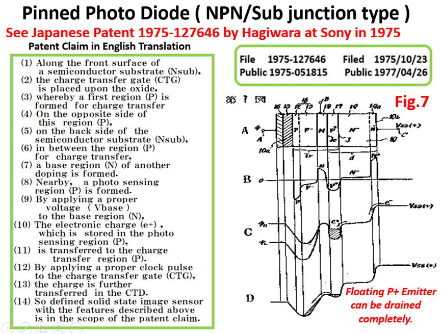
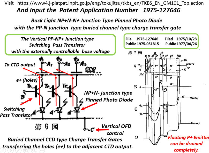
(5)Japanese Patent 1975-127646, filed on October 23, 1975
Invention of the N+NP+NP-P junction type Pinned Photodiode
with the P+NP junction type charge transfer gate to the CTD.
with the back light illumination scheme.
(6)Japanese Patent 1975-127647, filed on October 23, 1975
Invention of the N+NP+N junction type Pinned Photodiode
with the surface MOS type charge transfer gate to the CTD.
with the back light illumination scheme.
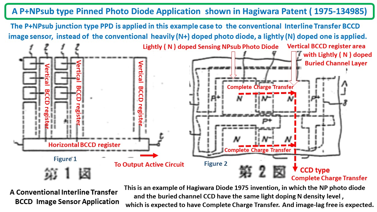
(7)Japanese Patent 1975-134985, filed on October 23, 1975
Invention of the P+NPNsub junction type Pinned Photodiode
with the built-in vertical overflow drain (VOD) function
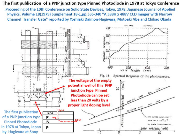
(8) “A 380Hx488V CCD imager with narrow channel transfer gates,”
by Y. Daimon-Hagiwara, M. Abe, and C. Okada, Proceedings of
the 10th Conference on Solid State Devices, Tokyo, 1978, Japanese
Journl of Applied Physics, vol. 18, supplement 18–1, pp. 335–340, 1979.
Hagiwara designed the Frame Transfer CCD image sensor alone with
the homemade design CAD tool that Hagiwara himself built, using FORTAN
programming software and with the company main frame computer.
Abe helped Hagiwara for the CCD chip fabrication.
Okada helped Hagiwara for the CCD chip testing.
Hagiwara was inveited to the internation CCD image sensor conference
to present his work on the P+NP junction photodiode at Edinburgh.
(9) Hagiwara, CCD'79 invited paper on "SONY Image Sensor Efforts"
at Edinburgh, Scotland UK on SONY CCD image sensors.
This is the first paper in the world reporting the P+NP type photodiode
with the Pinned surface potentail and complete charge trasfer to the CTD.
Hagiwara reported a very low dark current, the result of the surface pinning.
This paper is the origin of the SONY HAD(hole accumulation diode and
the Pinned Photodiode. Pinned Photodiode and SONY HAD both have the
pinned surface potential, which is the result of the hole accumulation in
the densely doped surface potential. This P+NP junction type photodiode
is based on the Hagiwara 1975 patent (1975-134985) of the P+NPNsub
junction type photodiode structure with complete charge transfer.
(10) "Interline Transfer CCD image sensor" with tranparent electrode and
complete charge transfer, by Kano, Ando, Matsumoto, Hagiwara and
Hashimoto, Japanese Television Society, Electon Device Reserch Coference,
ED481, pp.47-52, Jan 24, 1980.
Hagiwara designed the Interline Transfer CCD image sensor alone with
the homemade design CAD tool that Hagiwara himself built, using FORTAN
programming software and with the company main frame computer.
Kano and Matumoto helped Hagiwara for the CCD chip fabrication.
Ando and Hashimoto helped Hagiwara for the CCD chip testing.
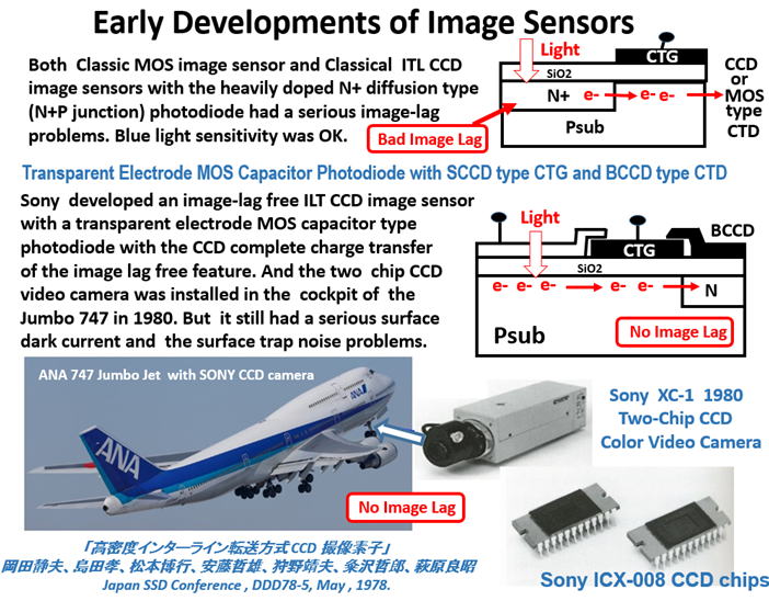
The two-chip set color video camera was sold to ANA and installed in
the cockpit of the Jumbo 747, introduing to the world a completely
image-lag-free action video camera.
SONY CCD top management people decided to concentrate their dilligence
to the mass production of the Interline Transfer CCD image sensor with
tranparent electrode with the lateral overflow drain.
SONY CCD top management people ignored Hagiwara 1975 patent invention
on the P+NPNsub junction type photodiode, which has a very low dark current
and very high blue light sensitivity, and besides the vertical overflow drain (VOD)
built-in structure can produce extra window area for more light sensitivity.
Hagiwara persistantly talked to SONY CCD top management people, institing that
his invetion of the P+NPNsub junction type photodiode is much better. But SONY
CCD top management people did not listen to Hagiwara. Finally, they fired Hagiwara.
Hagiwara had to move to another project sector and became the leader of a newly
organized Fast SRAM cache memory design team for digital CCD camera system.
Hagiwara and his team published the fast 4 Mega Bit Cache SRAM in ISSCC1989.
(11)Fumio Miyaji, Yasushi Matsuyama, Yoshikazu Kanaishi, Katsunori Senoh,
Takashi Emori and Yoshiaki Hagiwara, "A 25 nanosec 4 Mega bit CMOS
RAM with DYnamic Bot-Line Loads", ISSCC1989 and J.Solid State Circuits,
Vol24, No.5, October 1989.
This was the origin work of SONY Compact Digital CCD Image Sensor System Chipset.
Hagiwara was happy in the digital camera system team while SONY CCD top management
people suffered the large dark current related poor mass production technology problems.
The Interline Transfer CCD image sensor with tranparent electrode with the lateral
overflow drain had a serious problem of large dark current and very small light
window area because a large area was needed for the lateral overflow drain.
Hitachi had already MOS image sensor with the built-in vertical overflow drain(VOD).
NEC published in IEDM1982 the PNP junction type buried photodiode structure
in the Interline transfer CCD imager which has no image lag with the complete
charge transfer operation like the CCD type complete charge tranfer feature.
SONY CCD top management people finally decided to chage their target direction
and began to focus their dilligence on the P+NPNsub junction type photodiode
that was originally proposed persistantly by Hagiwara. Until then no one in Sony
understood the detailed features of Hagiwara invention and ignored Hagiwara.
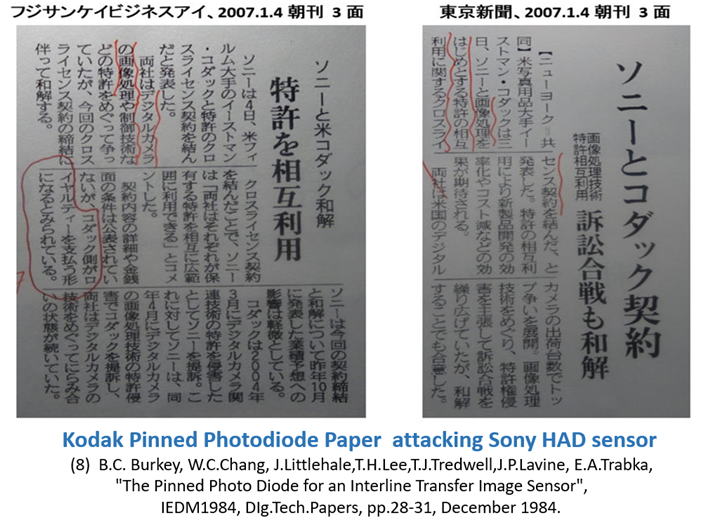
SONY and Hagiwara himself suffered by SONY-Fairchild, SONY-NEC and SONY-
KODAK patent wars on the CCD image sensor patents of the SONY HAD sensor.
SONY-Fairchild patent war (1991-2000) finally ended and Sony won over Fairchild.
Finally Hagiwara became happy and began to appear in the public.
Hagiwara recieved three invitations from the international conferences for his works.
(12) "SONY Consumer Electronics" by Yoshiaki Hagiwara,
ESSCIRC2001 invited paper, at Vilach, Austria, September 2001
(13) "SOI Cell Processor and Beyond" by Yoshiaki Hagiwara,
ESSCIRC2008 invited paper, at Edinburgh, Scotland UK, September 2008
(14)The 60th Aniversary ISSCC2013 Plenary Panel Talk, by Yoshiaki Hagiwara,
at San Franicisco, USA, February 2013.
********************
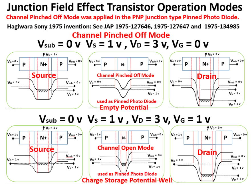
Hagiwara had five important ideas in 1975
for the pinned photodiode sensor structures.
********************
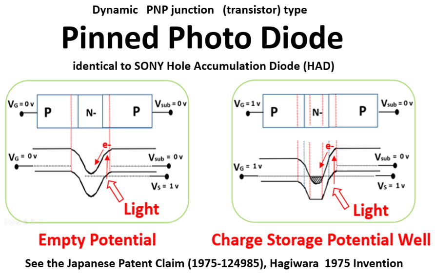
(1) Hagiwara invented P+NP/Sub junction
(thyristor) type Pinnned Photodiode
which is identical to Sony HAD Sensor
The substrate wafer can be either P-type,
N-type or intrinsic high resistivity one.
(2) Hagiwara invented the vertical overflow
drain (VOD) for the Pinnned Photodiode.
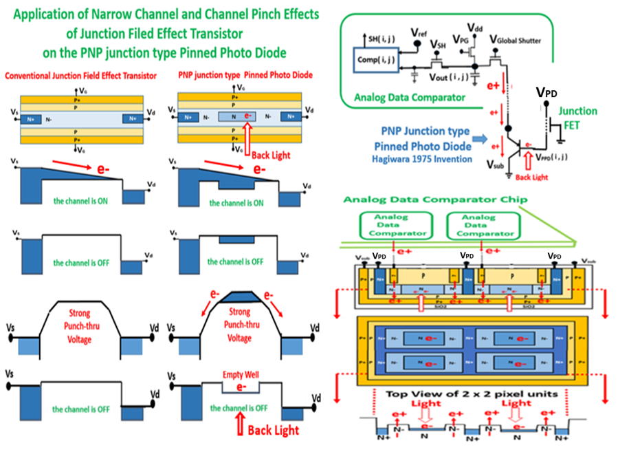
(3) Hagiwara invented the Back Light Illumination
Scheme for the Pinnned Photodiode
(4) Hagiwara invented the MOS capacitor type
Global Shutter buffer memory scheme
for the buried photodiode type Pinned Photodiode
with Back Light Illumination scheme.
(5) Hagiwara invented also the Schottky barrier
Photodiode for ILT CCD Image Sensor.
********************
********************
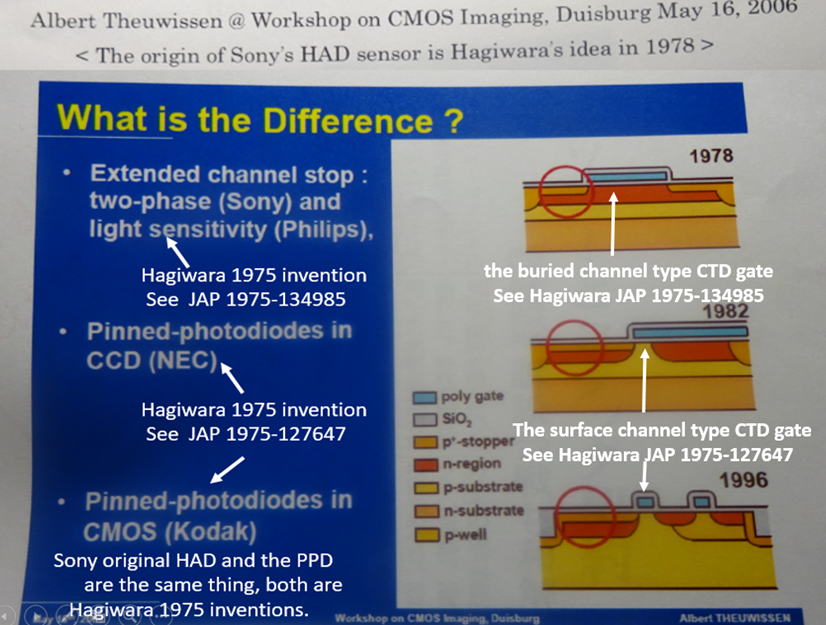
See the original 1975 Pinned Photodiode Patents
JP1975-134985 and JP1975-127647
filed and invented by Hagiwara at Sony in 1975.
The following two Japanese Patents
JP1978-1971 and JP1980-123959
are duplicate patents filed later than
the Hagiwara 1975 inventions shown above.
********************
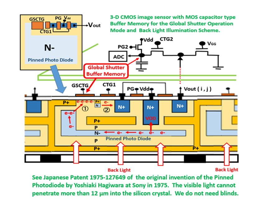
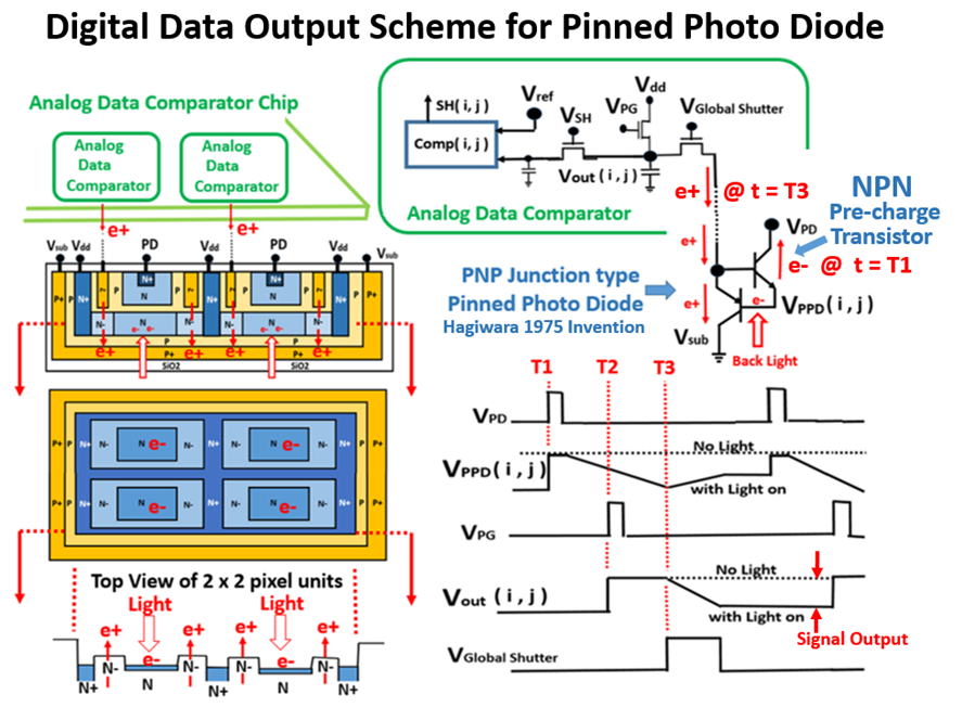
Conclusion : Hagiwara invented the Pinned Photodiode in 1975
in his two Japanese Patents ( 1975-127647 and 1975-134985)
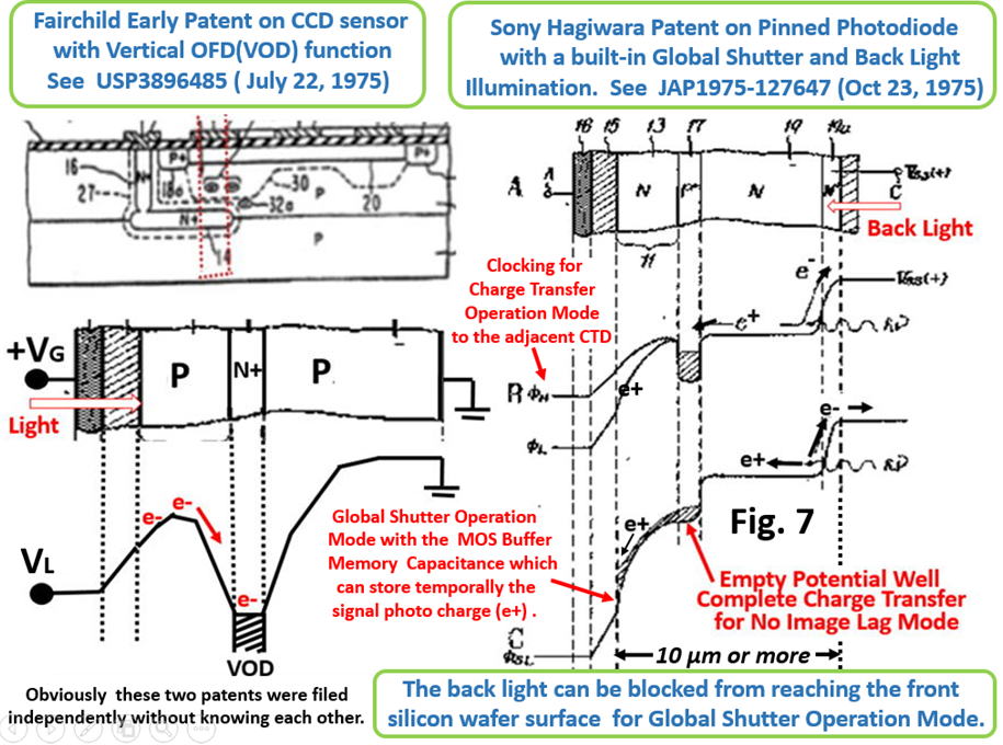
Hagiwara Patent 1975-127647 filed on Oct 22, 1975 defines
a NPN /Sub junction type Pinne Photodiode both with the
built-in Global Shutter Function of a MOS buffer memory
capacitance and also with the Back Light Illumination scheme.
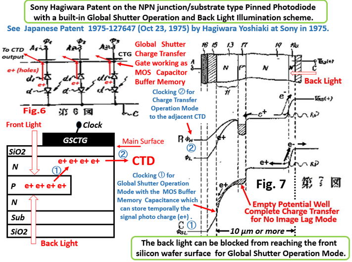
Note the difference from the normal usage of the charge transfer
gate. In this patent claim, the charge transfer gate is also used
as the short-time signal charge storage capacitance as the buffer
memory for the Global Shutter operation scheme. And later by the
second clocking the signal charge is transfered to the adjacent
charge transfer device(CTD). The CTD can be either a CCD type
CTD or a CMOS type CTD with active or passive circuits for each
pixel unit.
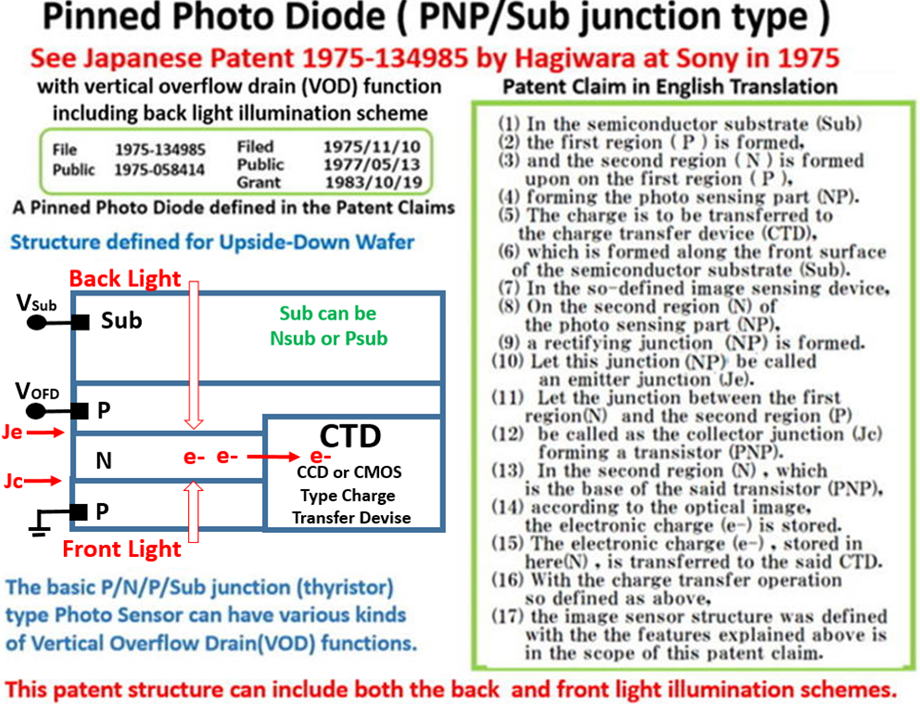
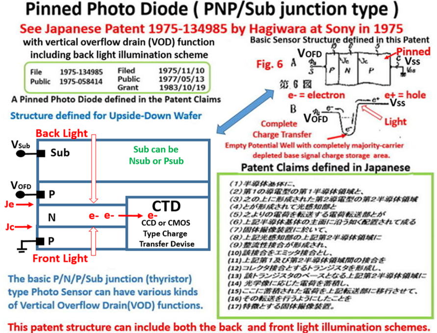
Hagiwara Patent 1975-134985 filed on Nov 10, 1975 defines
a PNP/Sub junction type Pinned Photodiode with the vertical
oveflow drain (VOD) function.
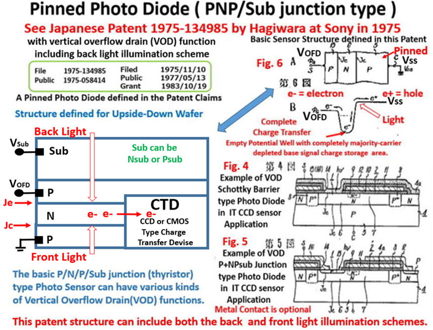
One possbile future application of the Pinned Photodiode.
Note that there are one on-chip P+N junction pinned photodiode buffer
memory and another the second stage buffer memory capacitance for the
double global shutter operations with two reset precharge switch gates.
The very lightly doped PN- junction pinned photodiode is applied as
the photo sensing initial photodiode, and the second fairly lightly doped
PN junction pinned diode is used the first stage buffer memory floating
diffusion for the first stage global shutter scheme. Note also that there
is another second stage global shutter buffer capacitance on the
separate chip before the A/D converter circuit with another second
stage precharge reset switch gate ( Walter Kosonocky invention 1972 )
See the original Pinned Photodiode Patent Japanese Patent 1975-134985
The first publication on the Pinned Photodiode ( SONY HAD Sensor ) in 1978.

**********************
Yoshiaki Hagiwara is the inventor of SONY original HAD sensor.
SONY HAD is defined as the P+/N/Pwell/Nsub junction type
thyristor photo sensing structure, originally invented by Yoshiaki
Hagiwara at SONY in 1975. See the 1975-134985 Japan Patent.
SONY HAD sensor (HAD1975) is identical to the P+NP junction
type Pinned Photodiode (PPD1980) with the NPNsub junction
type built-in Vertical Overflow Drain (VOD1978) Photodiode.
PPD1980 and VOD1978 are derivative of the Hagiwara 1975
invention of HAD1975 which is SONY original HAD sensor. .
Consequently Hagiwara (HAD1975) at SONY is the original and
true inventor of the Pinned Photodiode (PPD1980) and the
in-pixel built-in Vertical Overflow Drain Photodiode (VOD1978).
**********************
Story of Pinned Photo Diode (html)
See also ElectronicsStackExchangeSite on "What is Pinned Photo Diode
? "
Pinned Photo Diode was invented by Hagiwara of Sony in 1975 (PDF)
Hagiwara at Sony invented Pinned Photo Diode in 1975(PDF)
******************************************************************************
hagiwara-yoshiaki@aiplab.com
*******************************************************************
Please read the narratives about the CCD inventors.
https://www.dpreview.com/articles/3397331369/nobelprize
This artical says, "The CCD technology makes use of the
photoelectric effect, as theorized by Albert Einstein and
for which he was awarded the 1921 year's Nobel Prize.
By this effect, light is transformed into electric signals.
The challenge when designing an image sensor was to gather
and read out the signals in a large number of image points,
pixels, in a short time."
This statement is partly correct, but not exactly correct.
The device which transforms light into electric signals
is called as the photo sensor.
The device which gathers and reads out the electric signals
in a large number of image points, pixels, in a short time
is called as the charge transfer device(CTD).
CCD can act both as the photo sensing device and the
charge transfer device(CTD) and was the Super Star.
But the CCD type photo sensor was replaced by the
Pinned Photodiode developed by Sony in 1978, which
was based on Hagiwara 1975 invention of the P+NPNsub
junction type Pinned Photodiode with the vertical
overflow drain. Later NEC also replaced the CCD type
photo sensor by developping the P+NP junction
type Pinned Photodiode, which is identical to the
Hagiwara 1975 invention of the P+NPNsub junction
type Pinned Photo Diode.
SONY and NEC gave up already in early 1980s using
the CCD type photo sensor, and instead, used the
Pinned Photodiode which is highly-light-sensitive,
low-dark-current and low-image-lag, much better
than the CCD type photo sensor.
In1984 SONY successfully developped the SONY
original Hole Accumulation Diode (HAD) which is
the P+NPNsub junction type photo sensor, which
is Hagiwara 1975 invention.
As well known , the P+NPNsub junction is a thyristor
type structure , which is composed of two junction
type transistors.
One is the top part of the P+NPNsub junction,
which is the P+NP junction type photo diode, now
called also as the Pinned Photo Diode.
Hence, the Pinned Photo Diode is also included in
the Hagiwara 1975 invention of the P+NPNsub
junction type photo diode.
The other one is the bottom of the P+NPNsub junction,
which is the NPNsub junction type photo diode acting
as the vertical overflow drain (VOD) which was invented
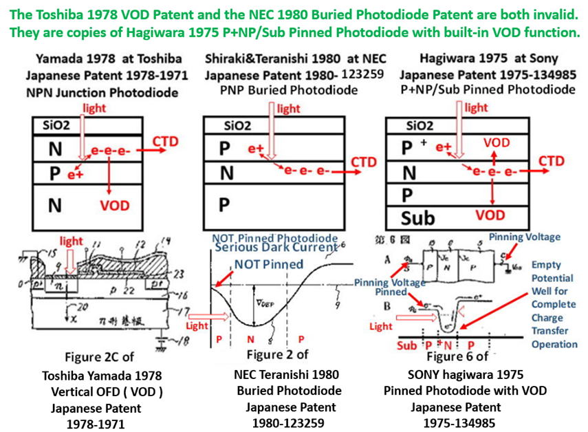
independently by Yamada at Toshiba in 1978.
But Hagiwara 1975 invention is earlier than Yamada
1978 invention and Teranishi 1980 invention. Both
Yamada 1978 invention and Teranishi 1980 invention
are not valid. They are duplicated copies of Hagiwara
1975 invention of the P+NPNsub junction type photo
sensing structure, which is now called as SONY HAD.
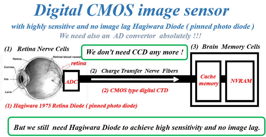
CCD is one type of CTD. Before CCD, MOS type CTD was
known. Now, CCD type CTD are completely replaced by
CMOS type CTD completely. Why ???
CCD is made of many MOS capacitors. The MOS capacitor
has the metal electrode. Metal type electrodes including
polysilicon electrodes are highly conductive with many
moving-electron charges that interact with, and reflect, light.
Metal does not let light pass thru the metalic electrodes.
Therefore CCD itself no way can become a good light
detecting photo sensor.
Hagiwara at SONY in 1975 invented the SONY HAD
sensor, which has a highly-light-sensitive, no-image-lag,
no-dark-currentand no-trap-noise photo sesnor structure
of theP+NPNsub junction type Pinned Photodiode with
the vertical over flow drain (VOD) structure.
See Japanese Patent 1975-134985.
Now, the CCD type CTD image sensors are completely
taken over by the CMOS type CTD imagers.
Now the CCD type CTD image sensors completely
disappeared from the image sensor world. Why ???
SONY and many other companies are not producing
CCD type CTD image sensors any longer. Why ????
TheCCD type CTD image sensor was the Super Star
during 1980s and 1990s. But now the CMOS type CTD
imager sensor is the Super Star. Why ??
Remember ?
A solid state image sensor has two important parts.
One is the light detecting structure that makes use
of the photoelectric effect, as theorized by Albert
Einstein and for which he was awarded the 1921
year's Nobel Prize.
By this photo-electron effect, light is transformed
into electric signals.
However, this CCD-type light detecting sturcture
was no longer used since early 1980s because SONY,
NEC and other companies replaced it with another
type of light detecting sturcture.
This CCD-type light detecting sturcture had many
disadvantages and poor performance.
The new photo sensing structure is now called as
the SONY original HAD ( hole accumualtion diode )
invented by Hagiwara at SONY in 1975, which is the
Pinned Photodiode with the in-pixel vertical overflow
drain (VOD) structure.
The other is the charge transfer device(CTD) that
was a big challenge when designing an image sensor
in order to gather and read out the signals in a large
number of image points, pixels, in a short time.
Historically we had a classical MOS type CTD without
in-pixel active curicuits until in 1966 Peter Nobel
invented the in-pixel active curicuits. However,
CMOS process technology was not well advanced.
Then, the CCD type CTD became the Super Star
as you know well. But after 50 years the CMOS
scale-down technology became well advanced.
We now can put the in-pixel active curicuits
invented by Peter Nobel in 1966 in each image
sensor picture element cell area.
And now the CCD type CTD image sensors were
completely replaced by the CMOS type CTD image
sensors. We no longer need the CCD type CTD
image sensors. We no longer need CCD completely.
However since Sony 1978 publication of the Pinned
Photodiode, we use still now the same light detecting
structure of the P+NPNsub junction type photodiode
that makes use of the photoelectric effect, as theorized
by Albert Einstein and for which he was awarded the
1921 year's Nobel Prize. By this photo-electron effect,
light is transformed into electric signals.
This light detecting sturcture is the SONY original
HAD(hole accumualtion diode) invented by Hagiwara
at SONY in 1975, which is the Pinned Photodiode with
the in-pixel vertical overflow drain (VOD) structure.
Hagiwara 1975 invention of the P+NPNsub junction type
photodiode makes use of the photoelectric effect, as
theorized by Albert Einstein and for which Albert Einstein
was awarded the 1921 year's Nobel Prize.
By this effect, light is transformed into electric signals.
This function was NOT performed by CCD at all since 1978,
because the CCD type photo sensor structure had many
disadvantages.
But the world called this image sensor with the Pinned
Photodiode sensor and the CCD type CTD, for a long
time, as a CCD image sesnor.
Now the world calls the image sensor with the Pinned
Photodiode sensor and the CMOS type CTD, for a long
time, as a CMOS image sesnor.
The world is completely ignoring the most important
lihgt-detencting sensor strucutre of the Hagiwara
1975 invention of the P+NPNsub junction type SONY
HAD sensor, which is the combination of the P+NP
junction type Pinned Photodiode and the NPNsub
junction type vertical overflow drain(VOD).
Hagiwara 1975 invention of the P+NPNsub junction type
photodiode was used since 1978 on, is being used till now
and will be used in future definitely, to transform light into
electric signals efectively, making use of the photoelectric
effect, as theorized by Albert Einstein and for which Albert
Einstein was awarded the 1921 year's Nobel Prize.
That is, CCD was NOT used as the device to transform light
into electric signals any longer in practical image sensor
applications in world wide, after the Hagiwara 1975 invention
of the P+NPNsub junction type photodiode, which is now called
as the Pinned Pinned Photo or by another name of the SONY
original HAD ( Hole AccumulationDiode).
The reasons are shown clearly in the above table. The CCD type
photo sensor structure had many disadvantages as shown above
table. The world gave up using CCD for the Pinned Photo Diode
as the light detecting photo sensor structure when SONY held
the Tokyo and New York Press Conference in 1978, where SONY,
for the first time in the world, published a low image lag, low
dark current, low trap noise , but highly light sensitive Pinned
Photodiode in the CCD type charge transfer device(CTD).
The challenge when designing an image sensor was to gather
and read out the signals in a large number of image points,
pixels, in a short time. For this purpose as a charge transfer
device(CTD), the buried channel CCD was the Super Star
since its charge transfer efficiency is close to 99.999% while
the surface channel CCD had only charge transfer efficiency
of 99.9 % was completely useless in 1970s.
Nowadays, the charge transfer efficiency of 99.999% of the
buried channel CCD also became completely useless for high
definition high resolution 8K and16K digital televion picture
qualities. Beside, CCD tyep CTD consumes a lot of power.
However, the Hagiwara 1975 invention of the Pinned Photo
Diode with the vertical Overflow Drain (VOD) function is
still valid and useful in the Modern CMOS type CTD image
sensors, which now have in-pixel active source follower
current amplifier circuits that was originally invented by
Peter Nobel in 1966. So CCD became completely useless.
Hagiwara invented, in his 1975 Japanese Patent 1975-134985,
the P+NPNsub junction type photodiode structure, which is
the origin of all the modern highly light-sensitive, low-noise,
low-dark current and low image-lag pinned photodiode with
the vertical overflow drain(VOD) structure.
This photo sensor was later in 1984 called as the SONY
original HAD ( Hole Accumulation Diode ) sensor right after
SONY successfully developed the mass production process
technology of this P+NPNsub junction type photodiode
structure for the first time in the world.
SONY took more than 9 years after the Hagiwara 1975 invention
simply because the P+NPNsub junction type photo diode needed
a very complex process technology which is the combination of
the classical bipolar process technology and the MOS process
technology dedicated to realize the CCD image sensor process.
However, SONY developed the P+NPsub junction type Pinned
Photo Diode without VOD for the first time in the world in 1978,
which is just an upper part of the Hagiwara 1975 invention of
the P+NPNsub junction type, which is a combined structure of
the P+NP junction type Pinned Photodiode with the NPNsub
junction type Vertical Overflow Drain (VOD) function structure.
In 1978, SONY published a FT CCD image sensor with the
P+NPsub junction type Photodiode which is now known as
the Pinned Photo Diode. It was the first publication of the
SONY HAD sensor, but it did not have the vertical overflow
drain (VOD) structure. Instead, a conventional lateral overflow
drain (OFD) was applied for this SONY HAD FT CCD image
sensor with the P+NPsub junction type Photodiode, which
is also now widely known as the Pinned Photo Diode.
Later in 1978, independently Yamada at Toshiba invented the
NPNsub photodiode with the vertical overflow (VOD) structure.
This is just the lower part of the Hagiwara 1975 invention of
the P+NPNsub junction type photo diode, which is a combined
structure of the P+NP junction type Pinned Photodiode with the
NPNsub junction type Vertical Overflow Drain (VOD) function.
So the VOD structure invented by Yamada at Toshiba in 1978
is a duplicatied copy of Hagiwara 1975 invention explained above.
Later in 1980, independently Teranishi at NEC invented the
P+NPsub junction type ( Buried layer ) Pinned Photodiode
But this is just the upper part of the Hagiwara 1975 invention of
the P+NPNsub junction type Pinned Photodiode which is a
combination of the P+NP junction type Pinned Photo Diode(PPD)
and the NPNsub junction type vertical overflow (VOD) structure.
So the VOD structure invented by Yamada at Toshiba in 1978
is a duplicatied copy of Hagiwara 1975 invention explained above.
Teranish at NEC published the no image lag ILT CCD image
sensor with the buried photo diode in IEDM1983.
However, SONY already published no image lag ILT CCD image
sensor in 1978 with the transparent electrode and lateral
overflow drain. SONY also developed and published the no image
lag FT CCD image sensor in 1978 with the Pinned Photo Diode
and with the lateral overflow drain.
Finally SONY developped SONY original HAD sensor in 1984,
which is a combination of the Pinned Photo Diode(PPD)
with the vertical overflow (VOD) structure for the first time.
in the world.
This combined structure of the PPD and VOD, is now known
as the SONY original HAD sensor, which is the Hagiwara 1975
invention, defined in Hagiwara Japanese Patent 1975-134985.
So it can be concluded that the Pinned Photodiode was invented
by Yoshiaki Hagiwara at SONY in 1975. Teranishi did not.
It can also be concluded that the vertical overflow drain(VOD) was
invented by Yoshiaki Hagiwara at SONY in 1975. Yamada did not.
To study and learn more about image sensors updated,
visit http://image-sensors-world.blogspot.com/
Here is a story of the world efforts
on early image sensor developments.
Original Photodiode and Phototransistor was invented
by John Northrup Shive in 1950 right after the invention
of bipolar transistor in 1947.
Invention History of Phototransistor and Photodiode
I am completely retired and no longer any expert.
But, once again, I am now trying to review and study
the image sensor world efforts.
(1) who is the original and true inventor of the Pinned Photodiode ?
(2) who is the one with the most significant contributions on
the CMOS type charge transfer devices (CTD) ?
As you know an image sensor is composed of two important parts.
One is the photo diode and the other is the charge transfer device(CTD).
The CCD type CTD was the Super Star but we no longer need it.
The CMOS type CTD is now working well with in-pixel amplifier circuits.
There are many quotations and narratives on Fossum and Teranish.
But I do not believe that Fossum is the major contributor of CMOS
Image sensor developments. I do not believe that Teranish is the
original inventor of the Pinned Photo Diode.
The following is my point of views on image sensor developments.
Original Photodiode and Phototransistor was invented
by John Northrup Shive in 1950 right after the invention
of bipolar transistor in 1947 as you know well.
Hagiwara was born on July 4, 1948 in Kyoto, Japan.
So, Hagiwara was maybe a single egg during the 1947
Christmas season when the transistor was invented.
Hagiwara left Japan in 1965 to live in Riverside, California
at age 17. Hagiwara was just a young high school student
at Riverside Polytechnic High School, very much interested
in science and technology, when Peter Noble invented
the in-pixel amplifiers in 1966.
Hagiwara moved to Pasadena, which is only 60 miles away
from Riverside, to study as an undergraduate student at
California Institute of Technology (Caltech) in Sept, 1967.
While Hagiwara was just a college student at Caltech, more
details were disclosed about image sensor elements with the
in-pixel amplifiers and were more intensively described by
Noble, and later by Chamberlain and by Weimer et al. in 1969.
At that time, passive-pixel sensors – that is, pixel sensors
without their own amplifiers or active noise cancelling
circuitry – were being investigated as a solid-state
alternative to vacuum-tube imaging devices.
Hagiwara was just a college student interested in
photo-transistors, while studying Feynman Physics
and the physics of semiconductor by Andy Grove.
Then, CCD was invented and became soon the Super Star
because CCD has the global shutter function and no image
lag features that can be applied to realize fast action motion
pictures while the MOS type charge transfer device (CTD)
needs an in-pixel extra buffer memory which was very
expensive to be included in each pixel.
In late 1990s, engineers in JPL at Caltech reported
the global shutter scheme for MOS image sensor
using the extra buffer memory in each pixel. But
the global shutter scheme was not their invention.
The pioneering image sensor engineers in 1970s all
knew the built-in global shutter function of the CCD
Super Star in 1970s. They all knew that CCD did
not need the extra expensive in-pixel buffer memory
while the conventional MOS image sensors needed one.
Hagiwara was a visiting professor of EE and Applied
Physics departments at Caltech. Hagiwara visited
often JPL and had frequent communications with
Dr. Pain's team of MOS image sensor working group.
They were not happy about Fossum's fraud actions.
Hagiwara did not understand the details.
But later Fossum published a 2013 fake paper
attacking Hagiwara 1975 patent by claiming that
Hagiwara 1975 PNP junction photo diode did not
have the complete charge transfer operation feature,
which was not true. And Fossum misled the world.
Hagiwara is finally convinced that Fossum is a fraud.
In late 1990s, as we all expected, CMOS scaled down
technology became so advanced, it became possible
to realize image sensor elements with in-pixel
amplifiers invented by Nobel. We all knew the trend.
This is not Fossum's idea. Fossum did nothing.
CCD type CTD image sensors are now completely
taken over by CMOS type CTD image sensors.
The CCD charge transfer efficiency of 99.999 % is
no longer enough to achieve the high definition
digital TV picture quality. CCD became useless.
It is well known that an image sensor is composed of
two important devices, one is the charge transfer
device (CTD) as described above, and the other is
the light detecting, photo sensing semiconductor device.
Especially, the light detecting, photo sensing structure
must be highly light sensitive, low trap noise, low dark
current and low image lag features with the high light
protection (VOD) capability.
This light detecting, photo sensing device structure
was invented by Hagiwara at SONY in 1975 in the form
of P+NPNsub junction type photo thyristor structure.
See JAP 1975-134985.
The P+NPNsub junction type photo thyristor structure
Hagiwara at Sony invented in 1975 has the hole accumation
Pinned P+ layer on the top of the P+NPNsub junction.
This was the origin of SONY HAD( Hole Accumation Diode)
developed by SONY in 1984.
Besides, as Hagiwara explained in the patent, as an
application example, this P+NPNsub junction structure
has inherently the built-in capability of vertical overflow
drain (VOD) capability.
It is well known that the P+NPNsub junction type photo
thyristor structure is composed of two junction bipolar
transistor structures.

One is the P+NP junction type photo transistor structure
and the other one is the NPNsub junction type photo
transistor structure.
In 1978 Hagiwara at SONY published the one chip color
FT CCD CTD type image sensor with the P+NP junction
type photo transistor structure, which later was cited as
the first publication of the Pinned Photo Diode by Prof.
Albert Theuwissen in his many technical presentations.
In 1978 Yamda at Toshiba filed a patent on the NPNsub
junction type photo transistor structure with the vertical
overflow drain (VOD) function. This structure is included
in the Hagiwara 1975 invention above.
In 1980 Teranishi at NEC filed a patent on the PNP
junction type photo transistor structure with the
buried N layer. But this PNP structure is included
in the Hagiwara 1975 invention above.
In 1983, Teranishi et al at NEC published the one chip color
ILT CCD CTD type image sensor with the P+NP junction
type photo transistor structure at IEDM1983. But no one
seemed to know that this PNP structure had been already
defined in the Hagiwara 1975 invention explained above.
At that time, SONY was working for the P+NPNsub junction
type photo diode of Hagiwara 1975 invention. In 1984, SONY
successfully developed the SONY original Hole Accumulation
Diode (SONY HAD) with the vertical overflow drain (VOD)
structure as originally defined in Hagiwara 1975 invention.
The world misunderstood that SONY developed SONY HAD
in 1984 following after Yamada 1978 invention and Teranish
1980 invention. But the truth is that SONY developed SONY
HAD in 1984 following after Hagiwara 1975 invention.
That is the reason why SONY called SONY Original HAD.
Prof. Kagami of Tohoku univ. pointed out in his technical
presentations that SONY HAD and Pinned Photodiode
are identical, the same thing that has two names.
At that time, SONY was the only company in the world
that had the mass production process line and technology
of the complex P+NPNsub junction type photo sensor.
SONY called the technology SONY HAD, but it was the
Hagiwara 1975 invention, which is the combination of
Teranishi 1980 invention of the Pinned Photo diode and
Yamada 1978 invention of the vertical overflow drain(VOD).
There it should be conclude that Teranishi 1980 invention
of the Pinned Photo diode is a copy of Hagiwara 1975
invention and also that Yamada 1978 invention of the
vertical overflow drain(VOD) is a copy of Hagiwara 1975
invention. Teranishi 1980 invention and Yamada 1978
invention must be copies, duplicatios or derivatives of
agiwara 1975 invention.
CCD image sensor mass production was possbile for
SONY because SONY already had the bipolar mass
process technolgy needed for signal processing bipolar
LSIs for SONY color homevideo and television sets.
NEC could not establish the mass production process
line and technology of the complex P+NPNsub junction
type photo sensor. Eventually, NEC gave up making CCD
image buisness while Panasonic never give up. Later
many companies were encouraged by SONY's success
and followed Sony. But remember that Sony image
sensor efforts exploded by Hagiwara 1975 invention.
Hagiwara at age 26 was the single engineer and scientist
designing and testing alone the image sensors in Sony.
He also had to develop in-house CCD design CAD tools
in a very small reserch team working at Sony Yokohama
Rearch Center under the leadership of Sony Pesident,
Iwama Kazuo, a bipolar transistor device physist at Sony.
(1) The Japanese Patent 1975-134985 shown below is
the evidence that Hagiwara at Sony is the inventor of
the Pinned Photo Diode and also that Hagiwara at Sony
is the inventor of the vertical overflow drain (VOD).
(2) The Japanese Patent ( 1975-127647) shown below is
the evidence that Hagiwara at Sony is the inventor of
the Pinned Photo Diode with the Back Light Illumination.
The details are explained below.
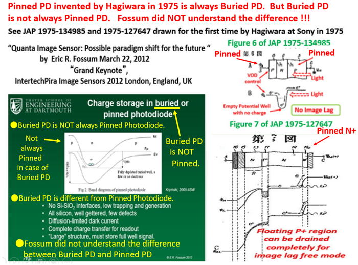
See the details in “ Quanta Image Sensor: Possible paradigm shift for the future “
by Eric R. Fossum March 22, 2012
“Grand Keynote”, IntertechPira Image Sensors 2012 London, England, UK
Hi Folks,
As you can see in the drawings attached above, the empty
potential well of the Pinned Photo Diode was drawn for the
first time in the world by Yoshiaki Hagiwara at Sony in 1975.
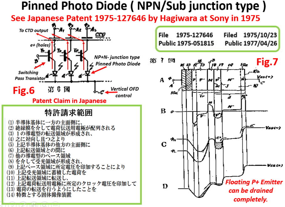
See the Fig. 6 of the Japanese Patent JAP 1975-134985 and
the fig.7 of JAP 1975-127647 respectively. Hagiwara wishes
that you all agree with Hagiwara that Hagiwara at Sony is the
true inventor of the Pinned Photo Diode.
As Fossum himself defined in his presentation the empty
potential well of the Pinned Photo Diode , you can see that
it is identical to the empty potential well that Hagiwara at
Sony drew in his patents in 1975. The Pinned Photo Diode
Is identical to the SONY HAD ( Hole Accumulation Diode),
too. A very few SONY people know this fact unfortunately.
Until June 2018, Hagiwara was not aware of what was
going on in the image sensor community because Hagiwara
was completely retired. After the ISSCC2013 plenary panel
talk, Hagiwara retired completely. Hagiwara was happy with
the last honorable presentation at the ISSCC2013 events.
Hagiwara thought he could now retire completely. Hagiwara
did not know what was going on in the last five years until in
June 2018 Hagiwara found the Fossum 2014 FAKE paper.
Hagiwara feels very sorry for having induced a large noise and
confused young generation engineers who are not aware of the
true history of image sensor developments. The image sensor
community and the IEEE EDS society made a lot of WRONG
citations and narratives on the inventor of Pinned Photo Diode
in the last five years after the 2014 Fossum FAKE paper..
The truth is that, the inventor of the Pinned Photo Diode is NOT
Teranishi-san although he did a good job for developing a large
scale IT CCD image sensor using the Pinned Photo Diode at NEC
But after the 1978 Sony Press Conference in Tokyo and New York ,
where one chip FT CCD image sensor camera using the Pinned
Photo Diode was announced, SONY was secretly preparing already
for mass production as the company top secret. After the CCD79
presentation at Edinburgh, Scotland UK, Hagiwara was convincing
the SONY TOP managements for the one chip IT image sensor using
the Pinned Photo Diode that Hagiwara defined in his 1975 patents.
See the Fig. 6 of JAP 1975-134985 and the Fig.7 of JAP 1975-127647.
As a visiting professor at Caltech in 1998 to 1999, when Hagiwara was
teaching graduate students in Applied Physics and Electrical Engineering
Departments, Hagiwara visited frequently JPL at Caltech , and met
many diligent engineers at JPL , including Dr. Pain, who were working
on the Active Pixel CMOS image sensors, while SONY was enjoying
a big business on CCD image sensors at that time. The CMOS image
sensor was NOT developed by Fossum alone. CMOS image sensors
were developed by many people, including Sony engineers. Hagiwara
himself alone did not develop the large scale image sensor either.
Many young and clever, diligent and silent, Sony engineers also worked
hard with back light illumination technology.
Hagiwara just invented the Pinned Photo Diode which is identical
to SONY HAD sensor. Hagiwara believes also that Hagiwara himself
invented the back light illuminated Pinned Photo Diode with the
vertical Overflow Drain (VOD). See the two Japanese Patent by
Hagiwara at Sony in 1975, JAP 1975-127647 and JAP 1975-134985.
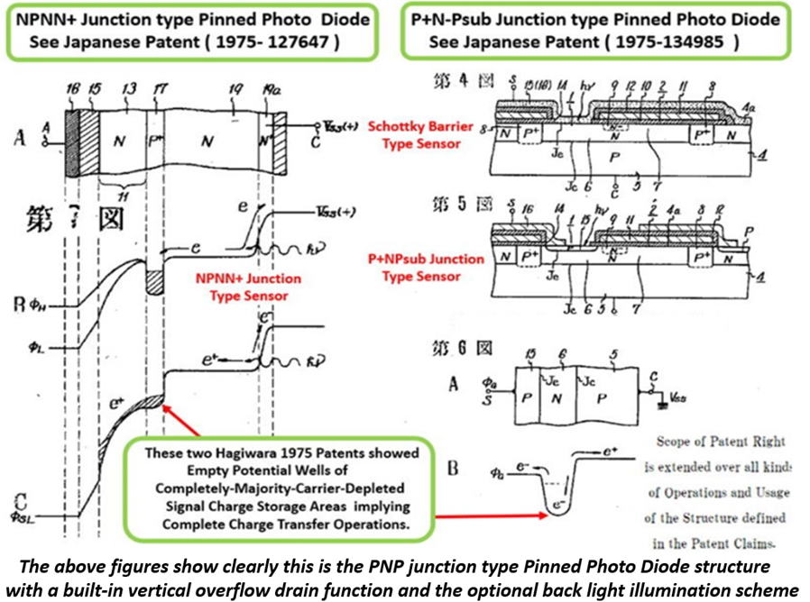
The above figures show clearly this is the PNP junction type Pinned Photo
Diode structure
with a built-in vertical overflow drain function and the optional back
light illumination scheme.
However, according to the official Japan Invention Web site,
Teranishi-san is cited as the inventor of the pinned photo diode ???
Yammada-san at Toshiba is cited as the inventor of the Vertical
Overflow Drain ??? And Suzuki-san at SONY is cited as the inventor
of the back illumination image sensor ??? Hagiwara is puzzled and
not happy on these citations and related public narratives.
Kind regards
Hagiwara, Yoshiaki
************************************
As seen in Japanese Patent 1975-134985, Hagiwara at SONY is the inventor
of the Pinned Photo Diode with the vertical overflow drain (VOD) structure,
Hagiwara at SONY is also the inventor of the Pinned Photo Diode with the
back light illumination scheme as seen in Hagiwara 1975 Japanese Patent
1975-127647 and 1975-127646. The details are explained below.
************************************
*******************************************************************
Pinned Photo Diode (PPD) and Hole Accumulation Diode (HAD)
PPD and HAD Story
*******************************************************************
Yoshiaki Hagiwara was invited in the following four international
conferences because of his contributions to the image sensor
community and related digital system LSI chip design works.
See the four invited talks related to the Pinned Photo Diode which is also
called as SONY original Hole Accumulation Diode (HAD) image sensor.
(1) International Conference CCD79 in Edinburgh, Scotland UK
See http://www.aiplab.com/0-CCD79_1979Hagiwara.pdf
(2) International Conference ESSCIRC2001 in Vilach, Austria.
See http://www.aiplab.com/ ESSCIRC2001.pdf
(3) International Conference ESSCIRC2008 in Edinburgh, Scotland UK
See http://www.aiplab.com/ 0-ESSCIRC2008Hagiwara.pdf
(4) International Conference ISSCC2013 in San Francisco, California USA
See http://www.aiplab.com/ ISSCC2013PanelTalk.pdf
(5) Pinned Photo Diode and SONY HAD are the same thing. Both were
invented by Hagiwara at Sony in 1975 in the Japanese Patents
(1975-127646, 1975-127647, 1975-134985).
See http://www.aiplab.com/Pinned_Photo_Diode_1975_invented_by_Hagiwara.pdf
(6) Hagiwara as a PhD student at CalTech designed a Fast 128 bit digital
data stream parallel comparator chip, which was fabricated at Intel
with the Intel 1101 PMOS process technology. Intel 1101 DRAM chip
was based on the Three MOS Transistor type source follower active
current amplifier circuit, which is very similar to the Active Three
MOS Transistor circuit applied to the current CMOS image sensors.
See http://www.aiplab.com/128_bit_Comparator.pdf
(7) Hagiwara designed a Fast 25 nanosecond access time 4 M bit Cache SRAM chip
for digital camera applications. Intel used the SONY SRAM chips in the Intel
boards. Sony enjoyed SRAM business while many companies in Japan were
focusing on the 4 M bit DRAM chip business.
See http://www.aiplab.com/SONY_4MSRAM_1989.pdf
*******************************************************************
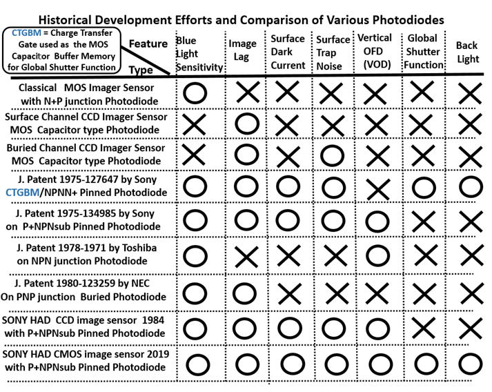
What is Pinned Photo Diode ?
Pinned Photo Diode is a light detecting photo diode structure
of a P+NP junction type in the substrate die which can be
applied to all kinds of the charge transfer device (CTD),
including CCD and CMOS image sensors. The signal electrical
charge is stored in the center N region. The surrounding top
P+ region is fixed or pinned to an externally controllable stable
voltage value. Both P+ and P region can be electrically connected
in common applications. Pinned Photo Diode is a dynamically
operating PNP junction. The center (buried) N region is floating
and dynamically operated. The top P+ region protects the base
N region from the top SiO2 surface trap interface states. Hence,
Pinned Photo Diode is free from the surface trap noise. Since
there is no SiO2 surface electric field, Pinned Photo Diode is
free from the surface electric field generated dark current.
The signal electrical charge is to be transferred to the adjacent
charge transfer device (CTD) thru the charge transfer gate with
complete charge transfer mode. This gives the feature of the
image lag free picture quality and more advantages as shown below.
Who invented Pinned Photo Diode ?
The pinned photo diode was originally invented and defined
by Hagiwara in the three 1975 Hagiwara patents. They are
( JAP 1975-127646, JAP 1975-127647 and JAP 1975-134985 ).
In these three Hagiwara 1975 patents, it was explained that
the light detecting structures defined in the patent claims
have many degrees of freedom in operational modes and also
can be applied , not only to the conventional frame transfer
and interline transfer CCD imagers but also to other charge
transfer devices, that include BBD and CMOS image sensor.
The completely image lag free Interline Transfer CCD image sensor
with the Pinned Photo Diode light detecting structure was invented
by Hagiwara in his 1975 patent applications. Teranish did not invent
the Pinned Photo Diode. Teranishi was one of the many developpers
of the Pinned Photo Diode, that include the diligent and hard working
Sony image sensor engineers including Hagiwara. Moreover, Teranish
did not invent the image lag free Interline Transfer CCD image sensor.
Teranishi was one of the many developpers of the completely image
lag free Interline Transfer CCD image sensor, that include the silent
and honest Sony image sensor engineers including Hagiwara. Hagiwara
invented the Pinned Photo Diode in 1975. Hagiwara invented also the
completely image lag free Interline Transfer CCD image sensor in 1975.
The first one is the Hagiwara JAP 1975-127646 in which the
PP-NP+NN+ junction type Pinned Photo Diode with Back Light
Illumination Scheme was defined with the PP-N type buried
channel charge transfer gate. The PP- layer is the buried channel.
Addition to that, the PP-NP+ junction functions as a switching
pass transistor with the P+ emitter as the floating charge storage
area while the base N region voltage is externally controlled.
The second one is the Hagiwara JAP 1975-127647 that defines
the N+NPN junction type Buried Photo Diode structure with
the surface channel type charge transfer gate with Back Light
Illumination. The signal charge stored in the P region can be
transferred completely.
The third one is the Hagiwara JAP 1975-134985 in which the
P+NPNsub junction (thyristor) type Pinned Photo Diode was
defined in the Patent Claim Scope with the charge transfer
gate of the buried channel type as an example in the ITL type
CCD image sensor type patent application example. In the patent
application examples, it is shown that the PNP jnction transistor
type structure has more degrees of freedom and can have
inherently the built-in vertical overflow drain (VOD) function.
Japanese Patent 1975-134985
Scope of Patent Claim in the original Japanese Text
(1) 半導体基体(A)に第1伝導型の第1半導体領域(B)と
この上に形成された第2伝導型の第2半導体領域(C)とが形成されて
(2) 光感知部(D)とこれ(D)よりの電荷を転送する電荷転送部(E)とが
上記半導体基体(A)の主面に沿う如く配置されて
(3) 固体撮像装置(F)において上記光感知部(D)の
上記第2半導体領域(C)に整流性接合(G)が形成され、
(4) 該接合(G)をエミッタ接合(H)とし、
(5) 上記第1(B)及び第2半導体(C)間の接合を
コレクター(I)とするトランジスタ(J)が形成し、
(6) 該トランジスタ(J)のベース(K)となる
上記第2半導体領域(C)に光学像に応じた電荷を蓄積し、
(7) ここに蓄積された電荷を上記転送部(E)に移行させて、
(8) その転送を行うようにしたことを特徴とする固体撮像装置(F)
Salient Key Words are defined below.
A = the semiconductor substrate (半導体基体)
B = the first region of the first conducting type (第1伝導型の第1半導体領域)
C = the second region of the second conducting type(第2伝導型の第2半導体領域)
D = the light detecting part(光感知部)
E = the charge transferring part(電荷転送部)
F = the solid state image sensor(固体撮像装置)
G = the rectifying junction(整流性接合)
H = the emitter junction(エミッタ接合)
I = the collector junction(コレクター接合)
J = the transistor structure(トランジスタ)
K = the base region(ベース)
Scope of Patent Claim in the English Translation
(1) In A, B and C are formed. C is formed upon B.
(1) A に B とこの上に形成された C とが形成されて
A = the semiconductor substrate (半導体基体)
B = the first region of the first conducting type (第1伝導型の第1半導体領域)
C = the second region of the second conducting type (第2伝導型の第2半導体領域)
(2) E transfers the electric charge from D.
D and E are placed along the main surface of the said A.
(2) D とこれ(D)よりの電荷を転送する E とが上記 A の主面に沿う如く配置されて
A = the semiconductor substrate (半導体基体)
D = the light detecting part (光感知部)
E = the charge transferring part (電荷転送部)
(3) In F, G is formed in C of the so-said D.
(3) F において上記 D の C に G が形成され、
C = the second region of the second conducting type (第2伝導型の第2半導体領域)
D = the light detecting part (光感知部)
F = the solid state image sensor (固体撮像装置)
G = the rectifying junction (整流性接合)
(4) The so-defined G is named as H.
(4) 該 G を H とし、
G = the rectifying junction (整流性接合)
H = the emitter junction (エミッタ接合)
(5) The junction between the so-said B and C is named as I. So J is formed.
(5) 上記 B 及び C 間の接合を I とする J が形成し
B = the first region of the first conducting type (第1伝導型の第1半導体領域)
C = the second region of the second conducting type(第2伝導型の第2半導体領域)
I = the collector junction (コレクター接合)
J = the transistor structure (トランジスタ)
(6) In the so-said C, which becomes K of the so-defined J,
the signal charge is stored according to the light image.
(6) 該 J の K となる上記 C に光学像に応じた電荷を蓄積し、
C = the second region of the second conducting type (第2伝導型の第2半導体領域)
J = the transistor structure (トランジスタ)
K = the base region(ベース)
(7) The charge stored in here is to be moved to the so-said E.
(7) ここに蓄積された電荷を上記 E に移行させて、
E = the charge transferring part (電荷転送部)
(8) So-defined F with the features of the charge transfer operation.
(8) その転送を行うようにしたことを特徴とする F。
F = the solid state image sensor (固体撮像装置)
Japanese Patent 1975-134985
Scope of Patent Claim in English Translation
(1) In A, B and C are formed. C is formed upon B.
(2) E transfers the electric charge from D.
D and E are placed along the main surface of the said A.
(3) In F, G is formed in C of the so-said D.
(4) The so-defined G is named as H.
(5) The junction between the so-said B and C is named as I.
So J is formed.
(6) In the so-said C, which becomes K of the so-defined J,
the signal charge is stored according to the light image.
(7) The charge stored in here is to be moved to the so-said E.
(8) So-defined F with the features of the charge transfer operation.
Salient Key Words are defined as
A = the semiconductor substrate (半導体基体)
B = the first region of the first conducting type (第1伝導型の第1半導体領域)
C = the second region of the second conducting type (第2伝導型の第2半導体領域)
D = the light detecting part (光感知部)
E = the charge transferring part (電荷転送部)
F = the solid state image sensor (固体撮像装置)
G = the rectifying junction (整流性接合)
H = the emitter junction (エミッタ接合)
I = the collector junction (コレクター接合)
J = the transistor structure (トランジスタ)
K = the base region (ベース)
Sony original Hole Accumulation Diode (HAD) and Pinned
Photo Diode (PPD) are the same thing. Both were invented
by Hagiwara in 1975. An example was given for a large area
ITL type CCD image sensor type patent application. But
applications are not limited to the ITL type CCD image sensor.
The patents can be applied to all kinds of charge transfer devices.
************************************************
In the Hagiwara 1975 patent claims, it was clearly stated that the proposed
light
detecting sensor cell structure, later called as Pinned Photo Diode which
is
identical to the SONY original Hole Accumulation Diode (HAD), can be applied
to all kinds of the charge transfer device (CTD), which includes the classical
MOS type image sensor, the FT and ILT type CCD image sensors and also the
modern CMOS active pixel image sensor.
In the Hagiwara 1975 patents, application examples were given only for
the ILT
type CCD image sensors. But the scope of the patent claims are not limited
by the appliation examples given in the patent explanations.
The application examples were given because the ILT type CCD image sensors
were most promising at that time. But as stated in the Hagiwara 1975 patent
claims, the scope of the patents includes all kinds of CTD.
The scope of the Hagiwara 1975 patent claims include, and hence can be applied
to, all kinds of the charge transfer device (CTD), including the classical
MOS
type image sensor, the FT type and ILT type CCD image sensors and also
the
modern CMOS active pixel image sensor.
Hagiwara filed two patent. One is JAP 1975-127647 with the N+NPN type Pinned
Photo Diode, with the surface channel type CTD gate as an application example.
And the other is JAP 1975-134985 with the P+NPNsub junction ( thyristor
) type
Pinned Photo Diode, with the buried channel type CTD gate as an application
example.
In these two patents, Hagiwara proposed both the Front Lihgt and the Back
Light
illumination type Pinned Photo Diodes in 1975..
In the Hagiwara 1975 patent claims, it was clearly stated that the proposed
light
detecting sensor cell structure, later called as Pinned Photo Diode which
is
identical to the SONY original Hole Accumulation Diode (HAD), can be applied
to all kinds of the charge transfer device (CTD), which includes the classical
MOS type image sensor, the FT and ILT type CCD image sensors and also the
modern CMOS active pixel image sensor.
In the Hagiwara 1975 patent, application examples were given only for the
ILT type CCD image sensor. But the scope of the patent claims are not
limited by the application examples given in the patent figures.
The ILT type CCD application example was given because the ILT type CCD
image sensors were most promising at that time..
*******************************************************************
See three invited talks related to SONY HAD sensor now called also as Pinned
Photo Diode.
(1) International Conference CCD79 in Edinburgh, Scotland UK
(2) International Conference ESSCIRC2001 in Vilach, Austria.
(3) International Conference ESSCIRC2008 in Edinburgh, Scotland UK
*******************************************************************
Hagiwara was invited in these international conferences because of his
contributions
to the image sensor community and related digital system LSI chip design
works.
*******************************************************************
*******************************************************************
Cool Facts of Image Sensor History
*******************************************************************
Cool Fact (1)
SONY announced in 1978 the one chip image-lag-free FT CCD image sensor
with the Pinned Photo Diode, Hagiwara 1975 invention. Hagiwara himself
designed the chip, developed the Pinned Photo Diode process fabrication
flow sequence and the CCD camera control system, all of them by Hagiwara
himself alone in 1976. Many doubted the success, but after the prototype was
made in 1977 by Hagiwara alone, many joined Hagiwara work and helped
Hagiwara and his original supporters..
Cool Fact (2)
The Pinned Photo Diod, Hagiwara 1975 invention whichis, in Sony, called
as
the SONY original HAD sensor, is still used in the modern digital CMOS
image
sensor with the back light illumination scheme which was proposed in 1975
by Hagiwara of SONY in Hagiwara Japanese Patent ( 1975-127647).
The Back Light Illumination type Pinned Photo Diode Sensor
invented by Haiwara of SONY. See Japanese Patent ( 1975-127647).
The Back Light Illumination type Pinned Photo Diode Sensor
invented by Haiwara of SONY. See Japanese Patent ( 1975-127647).
Cool Fact (3)
SONY announced in 1980 the two-chip image-lag-free IL CCD image sensor
with the picture cell structure of the transparent electrode with the lateral
overflow drain. The two chip type image-lag-free IL CCD video camera was
sold to ANA and was installed in the cock pit of the 747 jumbo jet. Hagiwara
designed and developed the two-chip image-lag-free IL CCD image sensor.
Cool Fact (4)
SONY won the SONY vs Fairchild Patent War ( 1991-2000 ) on the P+NPNsub
junction ( thyrisor ) type Pinned Photo Diode with the Vertical Overflow Drain
Function invented by Hagiwara( JAP 1975-134985 ).

Cool Fact (5)
SONY won the Secret Patnet War against the NEC Patent by Hagiwara 1975
P+NPNsub junction ( thyrisor ) type , completely image-lag-free Pinned
Photo
Diode Patent ( JAP 1975-134985) against the NEC 1979 Teranishi Patent
on the Buried Photo Diode which was published in IEDM198 by Teranishi.

Hagiwara did not understand why Fossum was insulting Hagiwara
and SONY pride and honor. Fossum is a fake commentator and
Fossum 2014 paper is a fake paper with WRONG conclusions.
Hagiwara and SONY engineers are not happy at Fossum and Teranish.
Cool Fact (6)
(Question)- who invented and developed the stitching technology
for large area image sensors ?
Hagiwara invented and Sony developed the stitching technology
for large area image sensors and named the technology as the
SONY original Hole Accumulation Diode (HAD) sensor.
Hagiwara invented it , in the Japanese 1975 patent ( 1975-134985 )
as the P+NPNsub junction ( Thyristor ) type Light Detecting Picture
Cell Structure which is now known widely as the Pinned Photo Diode.
As one of the Hagiwara 1975 patent application for large area image
sensors, Hagiwara drew in the Patent Figure the large scale Interline
Transfer CCD Image sensor as a possible application.
Sony deligent engineers, including Hagiwara, developed, the stitching
technology for large area image sensors. SONY called the technology
in SONY business as the SONY original HAD sensor . Naturally, the
technical world did not use the SONY business Brand Name HAD,
and called it by another name, the Pinned Photo Diode. But the
Pinned Photo Diode and SONY original HAD technology are the
same thing, both invented by Hagiwara in 1975.
Teranishi did not invent the Pinned Photo Diode.
Hagiwara is the inventor of the Pinned Photo Diode.
Cool Fact (7)
(Question) - who owns the world record in low-noise
in the voltage domain for CMOS Image Sensor (CIS) ?
Sony deligent engineers developed and now Sony owns
the world record in low-noise in the voltage domain for CMOS
Image Sensor (CIS) with the Pinned Photo Diode with the
Back Light Illumination, that was also invented by Hagiwara of
SONY in 1975 the Japanese 1975 patent ( 1975-127647 ).
Fossum did not develop the modern digital CMOS image sensor
The Sony deligent engineers developed the modern digital CMOS
image sensor.
Fossum is not the inventor of the active image sensor picture
element. Peter Noble is the inventor of the active image sensor
picture element. See http://www.pjwn.co.uk/
Cool Fact (8)
(Question) - Who won on the SONY-Kodak Patent War on Digital Camera ?
SONY and Kodak made an agreed in 2007 to use each other's patents.
Digital Camera by definition must be small and handy as originally conceived
by SONY with many semiconductor components including the image sensor,
ADC, Fast Cache SRAM, the slow Nonvolatile memory chip and other digital
image processing units. One single engineer cannot develop all of it alone.
Many SONY deligent enginneers worked hard and developed the modern
CCD and CMOS digital Camera, with the P+NPNsub junction (thyristor)
type Light Dectecting Photo Diode ( JAP 1975-134985 ) and the N+NPN
junction type Buried Photo Diode ( JAP 1975-127647 ) with the back
light illumination scheme, both invented in 1975 by Hagiwara of Sony.
One person can invent it, but the many years of the hard working efforts
of many deligent people are needed to realize it.
*******************************************************************
*******************************************************************
Brief History of Image Sensors.
*******************************************************************
In 1960s, before CCD was invented, we already had beautiful color pictures
by the classical MOS image sensor with an excellent light sensitivity obtained
by the classical N+P junction type photo diode.
But to overcome the very large wire (CkT) noise, the three transistor
active source follower type circuits, invented by Peter Noble, was needed.
But the picture cell area was too small to incorporate this active circuit
in each picture cell area. We all knew that we had to wait untill we have
the complete MOS transistor process scale down, much furthur down.
(2) However, the CCD invention gave the image lag free and very low
wire (CkT) noise pictures. The CCD became the super star with the
help of the P+NPNsub junctiion (thyrsitor) type photo diode, which
was invented by Hagiwara in 1975. See JAP ( 1975-134985 ) .
CCD consumed a lot of power with only the transfer efficency of 99.999
%,
which was however possible to be applied for the classical NTSC picture
resolution. CCD had the serious trap noise and surface dark current problems.
Moreover, CCD had inherently MOS metal-type electrodes that do not pass
light and CCD was not as light-sensitive as the N+P photo diode. So, the
CCD
type light detecting picture cell was replaced by the the P+NPNsub junctiion
(thyrsitor) type photo diode, Hagiwara 1975 invention. See JAP ( 1975-134985 ) .
In 1978, SONY annouced in New York and Tokyo Press Conferences the world
first CCD image sensor with no image lag, very highly light sensitive,
low trap
noise, low surface dark current features of the PNP junction type photo
diode
sensor pixel structure,Hagiwara 1975 invention. See JAP ( 1975-134985 ) .
At that time, the world already gave up the CCD image development efforts.
SONY was the only company that never gave up. Sony showed the future of
CCD image sesnor applications. The truth is that Hagiwara in SONY was the
only engineer in the world who did not give up. And Hagiwara showed the
future of CCD image sesnor applications. by the P+NPNsub junctiion type
photo diode, Hagiwara 1975 invention. See JAP ( 1975-134985 ) .
So Hagiwara save the CCD by his 1975 invention, which is now called by
another name, the Pinned Photo Diode.
The truth is that CCD was NOT highly light sensitive, NOT low dark current
and NOT trap noise free image sensor structure. The true super star was
not CCD. The true super star was hiden behind the curtain. The true super
star was Hagiwara 1975 invention, which is now called by another name,
the Pinned Photo Diode. SONY called it as the SONY original HAD sensor.
The truth is that the Pinned Photo Diode and the SONY original HAD sensor
are the same thing, that Hagiwara of SONY invented in 1975.
In conclusion, Hagiwara of SONY invented and his team of many dilligent
and hard working SONY engineers developed the stitching technology
for large area image sensors. The world followed after SONY efforts.
(3) Now, the complete CMOS transistor process scale down was achieved.
And the scale-downed three transistor active source follower type circuits,
originally invented by Peter Noble, can be now easily incorporated in each
picture cell of the CMOS image sesnors, with the help of the P+NP junctiion
type photo diode with the back light illumination scheme, which is again
the
invention by Hagiwara in 1975. See JAP( 1975-127647 ).
SONY diligent and hard working engineers developed the modern dgital
CMOS image sensor with the back light illumination scheme for the
first time in the world.
Now again SONY owns the world record in low-noise in the voltage domain
for the modern digital CMOS image sensors (CISs).
Hagiwara 1975 invention ( JAP 1975-134985 ) helped CCD image sensor
in the past. Hagiwara 1975 invention ( JAP 1975-127647 ) is helping CMOS
image sensor now. Hagiwara and his original team of SONY diligent and hard
working engineers developed the stitching technology of both CCD and
CMOS large area image sensors.
CCD was considered as the Super Star in the image sensor world in the past,
and the inventors were awarded with the NOBEL prize. But now CCD has
completely dissappeared from the modern digital image sensor world.
So who were the real super stars in the world ?
And now who are the real super stars in the world ?
*******************************************************************
Dear Friends, July 28, 2018
Hi, my name is Yoshiaki Hagiwara, an ex-Sony man.
I worked at Sony from 1975 until 2008.
I was also a visiting professor at CalTech from 1998 t o 1999.
I retired from Sony in 2008.
I was invited in the ISSCC2013 plenary panel.
Hagiwara at SONY invented the pinned photo diode in 1975.
See the two Japansese patents below which was filed by Hagiwara in 1975.

As you can see clearly in the Fig. 7 above, the N+NPN junction type
Pinned Photo Diode can be operated in the Complete Charge Transfer
Mode.
This important Complete Charge Transfer Mode Opertaion is also shown
in the Fig.6B of the PNP junction type Pinned Photo Diode Application
shown below.
I believe Hagiwara myself invented the Pinned Photo Diode.
I believe Teranishi did not invent the Pinned Photo Diode.
*******************************************************************
Questions by Prof. Albert Theuwissen are ,
- who invented and developed the stitching technology
for large area image sensors ?
- who owns the world record in low-noise
in the voltage domain for CMOS Image Sensor (CIS) ?
*******************************************************************
Hagiwara believes that
Hagiwara invented it , in the Japanese 1975 patent ( 1975-134985 ) as the P+NPNsub
junction ( Thyristor ) type Light Detecting Picture Cell Structure, and Sony diligent
engineers, including Haggiwara, developed, the stitching technology for large area image
sensors. SONY called it as the SONY original HAD sensor technology in SONY business.
Naturally, the technical world did not use the SONY businesss Brand Name HAD, and
called it by another name, the Pinned Photo Diode. But the Pinned Photo Diode and
SONY original HAD are the same thing, both invented by Hagiwara in 1975.
At least, Teranishi did not invent the Pinned Photo Diode.
Hagiwara is the inventor of the Pinned Photo Diode.
Sony diligent engineers developed and now Sony owns
the world record in low-noise in the voltage domain for CMOS Image Sensor
(CIS)
with the Pinned Photo Diode with the Back Light Illumination, that was
also invented
by Haiwara of SONY in 1975 the Japanses 1975 patent ( 1975-127647 ).
At least, Fossum is not the inventor of the active image sensor picture
element.
Peter Noble is the inventor of the active image sensor picture element.
http://www.pjwn.co.uk/
In the Fossum 2014 fake paper, Fossum attacked Hagiwara 1975 patent
with lies, insulting Sony and Hagiwara honor and pride on purpose.
I could not understand Fossum motivation.
But I am now convinced that Fossum wanted Fossum himself
to be recognized by the world, with false explanations. Fossum
used Teranishi as the FAKE inventor of the Pinned Photo Diode,
Fossum wanted to convince the world that Fossum himself
developed the modern CMOS digital camera.
But now I understand that Peter and SONY diligent engineers
including Hagiwara. This is not fair at all. It is all lies.
The world should know the truth.
Until last June I did not know what is the Pinned Photo Diode.
I knew SONY HAD. But I did not know myself that SONY HAD
and the Pinned Photo Diode are the same thing.
My friends in Sony informed me that Teranish received awards
from Queen Elizabeth and Japanese Emperor as the inventor
of the Pinned Photo Diode.
SONY diligent engineers were not happy at all.
So I began to study what is Pinned Photo Diode last June.
Then I found the Fossum 2014 fake paper.
I became really MAD at Fossum.
Besides, SONY won the SONY-NEC Patent war by Hagiwara 1975 patent
against the Teranishi1979 patent a long time ago. So Teranish should
know that Hagiwara is the inventor even though Teranishi published
his work in IEDM1982.
Teranishi work was just a copy of Hagiwara 1975 patents that defined
as one example case of Interline CCD image sensor with the complete
charge transfer mode ( no image lag ) P+NPNsub junction type photon
detector structure, which is now called as the Pinned Photo diode.
But it is now more than four years after Fossum 2014 fake paper publication.
I found this fake paper, really too late.
I was very, very late since I do not belong to
the image sensor community any more.
Yes, with my interests in the intelligent image sensors
included, but my current major interests are
in the AIP ( Artificial Intelligent Partner ) systems,
including AI software and AI digital circuit system applications.
Yes, I try to be calm, but cannot be silent.
I feel that the world should know at least what is the truth.
I don’t think I can change the past history.
But people can learn the truth anytime, now and in future.
Yes, many people contributed.
Their diligence and efforts must be much worth recognitions.
*******************************************************************
http://www.aiplab.com/Hagiwara_at_Sony_is_the_true_inventor_of_Pinned_Photo_Diode.html
http://www.aiplab.com/Story_of_Pinned_Photo_Diode.html
http://www.aiplab.com/
*******************************************************************
*******************************************************************
********************************************************************
Evidence that Hagiwara at Sony is the true inventor of the Pinned Photo Diode
*******************************************************************
Evidence that Hagiwara at Sony is the true inventor of the Pinned Photo Diode
is given by the two Japanese patents Hagiwara filed in 1975 at Sony. They are,
Japanese Patent (1975-127647) and (1975-134985). The evidence is described in
details in these two Hagiwara 1975 Japanese patents.
In 1978 Sony announced a new video camera in Tokyo and New York
Press Conferences at the same date, held by Sony Chairman
Akio Morita in New York and Sony President Kazuo Iwama
in Tokyo at the same date in 1978.
The video camera was built with the Frame Transfer CCD image
sensor with the Hagiwara invented Pinned Photo Diode light
detecting photo sensing picture cell structure which has a very
high light sensitivity, a very low trap noise, a very low dark current
and a very low image lag features.
The figures N0.1 thru No.5 in Hagiwara Japanese patent (1975-134985)
explained in details an example of the interline transfer CCD image
sensor application with the Hagiwara invented Pinned Photo Diode.
Sony engineers, after the 1978 Press Conferences in Tokyo and New
York, worked hard for, and succeeded to acquire, the production
and the reliability technolgy of the CCD video camera of the interline
transfer CCD image sensor application with the Pinned Photo Diode
light detecting picture cell structure with the vertical overflow function.
With the diligent SONY engineers efforts, SONY could produce the
portable Passport size Compact CCD image sensor video camera, with
the Pinned Photo Diode that Hagiwara invented in 1975.
And at the same time, Sony filed a trading name officially, which
is the SONY Brand Name of " Sony original HAD sensor " .
With the help of the Hagiwara invented Pinned Photo Diode, which
was now called as " Sony original HAD sensor " with the strong
SONY original sales features of high light sensitivity, low noise and
no image lag characteristics, Sony could become soon very dominant
and strong over the world consumer video camera markets.
The feature of no image lag characteristics in the Hagiwara invented
Pinned Photo Diode is explained and shown in details, as an example
application case, in the figure No.6 of Hagiwara 1975 Japanese Patent
( 1975-134985 ) and also in the figure No.7 of Hagiwara 1975 Japanese
Patent ( 1975-127647 ) in details.
Hagiwara 1975 Japanese Patent ( 1975-127647 ) proposed a Back Light
illumiantion type light detecting photo sensing picture cell structure
with the buried layer type photo signal charge storage. And in the
figure No.7 of Hagiwara 1975 Japanese Patent ( 1975-127647 ) was
shown clearly how the signal charge in the buried storage layer are
trasfered completely to the region under the charge transfer gate
formed on the front side of the silicon wafer. This means clearly
the light sensing picture cell structure, which is now worldly called
as the Pinned Photo Diode, has the very important feature of no
image lag characteristics.
All of these Patent Claim descriptions and Patent figures for possible
patent application examples given in details in the two Hagiwara 1975
Japanese Patents ( 1975-127647 ) and ( 1975-134985 ) support the fact
that Hagiwara is the true inventor of the Pinned Photo Diode.
In conclusion, it is a clear cool fact that Hagiwara at Sony is the true
inventor of the Pinned Photo Diode. The Haiwara patents claims that
the light detecting picture cell structure ( now called as the Pinned
Photo Diode ) can be applied to any kind of charge transfer device(CTD)
which includes the BBD type, the classical MOS type, the CCD type and
the modern CMOS image sensor type charge transfer devices.
Hagiwara proposed the Pinned Photo Diode with the P+NPNsub junction
(thyrisor) type Light detecting picture cell structure with the vertical
over flow drain for the first time in the world.
Moreoever, Hagiwara proposed in the Japanese patent application example
of figure No.7 of Japanse patent (1975-126747) the Back Light illumination
Pinned Photo Diode type Light Detecting Picture Cell Structure for the
first time in the world.
Moreoever, Hagiwara proposed in the Japanese patent application example
of figure No.4 of Japanse patent (1975-134985) the Schottky Barrier type
Light Detecting Picture Cell structure in the Interline transfer type
CCD image sensor applicaiton for the first time in the world.
**************************************************************************
However last year Hagiwara learned a very surprising news:
**************************************************************
2017 Queen Elizabeth Prize for Engineering Foundation.
**************************************************************
The winners of the 2017 Queen Elizabeth Prize
for Engineering Foundation were :
(1) George E. Smith for the CCD image sensor invention
(2) Michael Tompsett for the CCD image sensor development.
(3) Nobukazu Teranishi for the invention of the pinned photodiode (PPD)
and
(4) Eric Fossum for developing the CMOS image sensor.
**************************************************************
Hagiwara, the true inventor of the Pinned Photo Diode, got really
surprized at the announcement that Teranishi was awarded for the
invention of the pinned photodiode(PPD), and many SONY dilligent
engineers working for the compact digital CMOS image sensors
got really surprized at the announcement that Fossum was awarded
for developing the CMOS image sensor. The truth is that Teranish
did not invent the PPD. Teranish only developped in 1982 the image
lag free interline CCD image sensor with the PPD light detecting
photo sensor structure that was invented by Hagiwara in 1975.
Hagiwara 1975 patents clearly defined the image lag free interline
transfer CCD image sensor as an application example of his 1975
patent claims.
Fossum wrote a paper on "Active Pixel Sensors: Are CCD's
dinosaurs ?" , in Proc. SPIE, Vol.1900, pp.2-14, 1993. However,
the three transistor type active circuit was already invented by
Bill Regitz of Honeywell in 1969. This active pixel sensors was
not Fossum invention. Fossum actually did not develop the
active pixel sensors either. Sony dilligent engineerings did.
Fossum is not the inventor of the active image sensor picture element
at all.
Peter Noble is the true inventor of the active image sensor picture element.
http://www.pjwn.co.uk/
Hitachi MOS Image Sensor Engineers and Intel MOS Process
Engineers all knew that eventually scaled down MOS Process
Technology will conquer all other kinds of Process Technologies
including CCD image sensor technology because of the power
consideration and scaled down dimensional advantage of CMOS
process technology. The three transistor CMOS active picture
cell was already invented as, since the three-transistor circuit
is identical to, the three-transitor circuit of the DRAM cell with
the active source follower type current amplification. Fossum
was just a commentator in his SPIE 1993 paper above. Fossum
was just emphasizing the well understood fact and speculations
that the original image sensor experts all knew in 1970s. This
active pixel sensors was not Fossum invention.Fossum actually
did not develop the active pixel sensors either.
Sony dilligent engineerings developped the active pixel Pinned
Photo Diode type Light detecting photo sensors for compact
digital CMOS image sensors with the Back Light Illumination.
**************************************************************
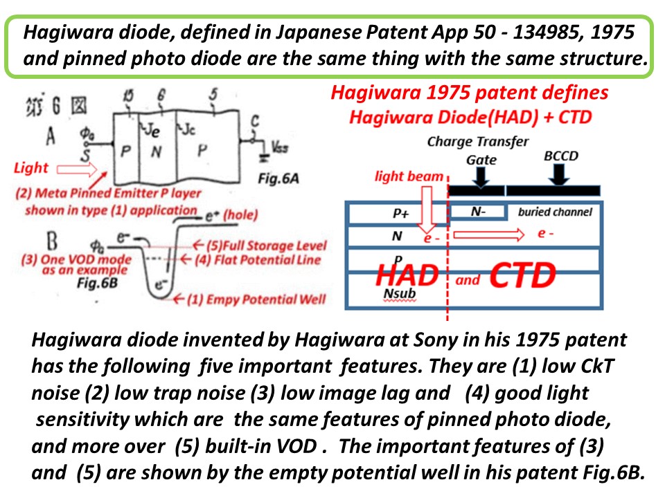
These patents show that Hagiwara is the inventor of Pinned Photo Diode.
Hagiwara showed that the CCD unique feature of Complete Charge Transfer
Mode was not unique at all. The pinned photo diode (PPD) invented by
Hagiwara also have this very important feature of Complete Charge Transfer
Mode. Besides, the PPD invented by Hagiwara has much better light sensitivity
because the top layer of the PPD sensor area is exposed and covered with
the SiO2 glass like layer . And light can freely pass thru the SiO2 glass like layer.
This is much better than CCD sensors which have poor light sensitivity
due
to the metal electrodes on the top layer in CCD sensors that do not let
light
pass thru.
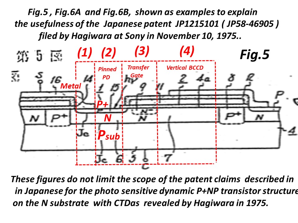

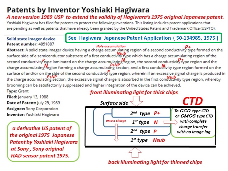
The world does not know the empty potential well
that Hagiwara drew for the first time in the world
in the PNP junction type photo sensor structure (Hagiwara Diode)
that is now also known as pinned photo diode.
The empty potential well is shown below in Fig.6B of Hagiwara 1975 Patent.
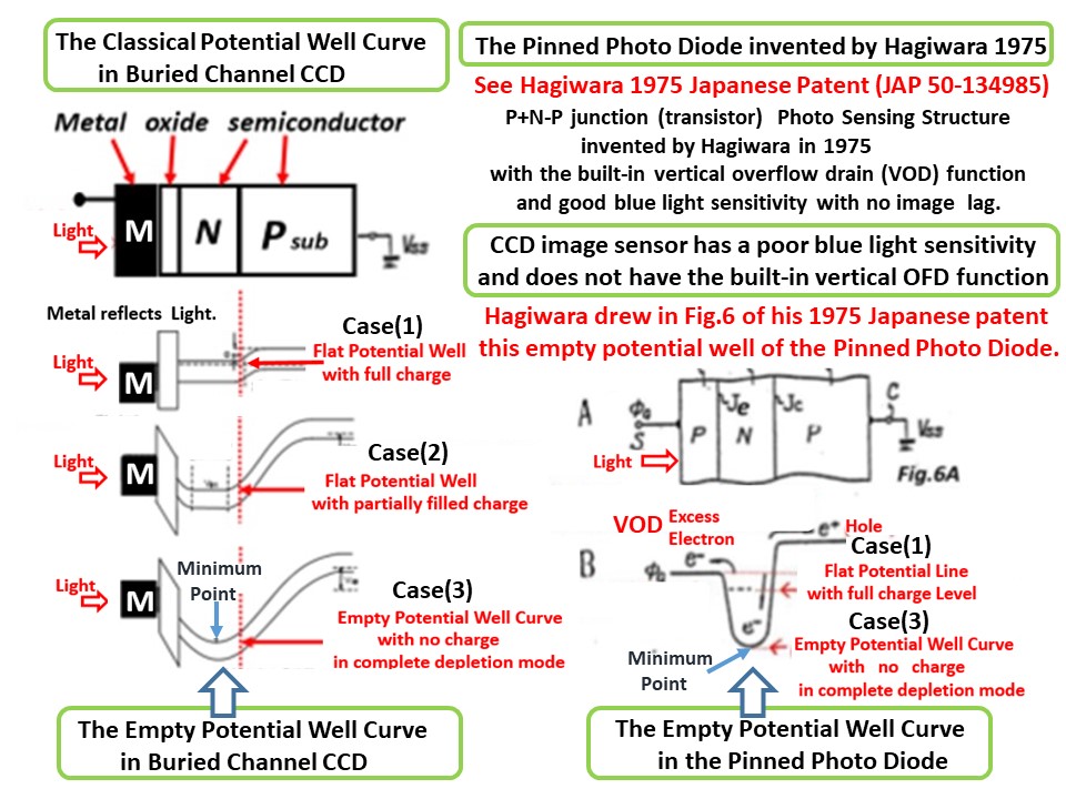
The empty potential well is the result of
the complete charge transfer of the photo electrons
to the adjacent CTD , which implies no image lag high quality pictures.
CTD ( charge transfer device ) described in Hagiwara 1975 patent
can be a CCD type CTD and also a CMOS type CTD.
Hence Hagiwara is the true inventor of the pinned photo diode
which can be applied for both CCD image sensors and CMOS image sensors.
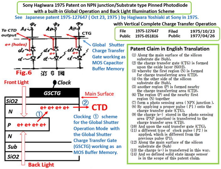
From the evidence shown above, it is clear that Hagiwara at SONY invented
the pinned photo diode in 1975. See the two Japansese patents above
which was filed by Hagiwara in 1975. However, I am now not very happy.
The reason is explained below in details.......
***********************************************************************
Recently I learned about the winners of
2017 Queen Elizabeth Prize for Engineering Foundation.
***********************************************************************
The winners of the 2017 Queen Elizabeth Prize for Engineering Foundation were :
(1) George E. Smith for the CCD image sensor invention
(2) Michael Tompsett for the CCD image sensor development.
(3) Nobukazu Teranishi for the invention of the pinned photodiode (PPD) and
(4) Eric Fossum for developing the CMOS image sensor.
***********************************************************************
I was surprised that Teranishi and Fossum are the two of the four winners.
I don't think that Teranishi invented the pinned photo diode in 1983.
Hagiwara at Sony invented the pinned photo diode in 1975 in his Japansese patent.
I don't think Fossum developped the modern CMOS image sensor.
I think the diligent and silent hard working SONY young engineers developed
the modern CMOS digital image sensor with the Back Light illumination.
Fossum did not invent the three transistor active circuits. The active
circuit
was invented by Rigitz of Honeywell in 1969 and was applied in the Intel
1101
DRAM chip of the three transistor formation of the active source follower
circuits.
Fossum did NOT invent the active source follower circuit.
Bill Regitz of Honeywell invented it in 1969 as shown above.
Fossum did NOT develop the CMOS digital image sensor at all.
Teranish did NOT invent the Pinned Photo Diode, either.
.
The Teranishi 1983 paper on NEC buried photo diode ILT CCD imager is
the same device that Hagiwara defined in Hagiwara 1975 Japanese patent.
I don't think that Fossum developped the CMOS image sensor alone.
Fossum is not the main contributor of developping the digital CMOS image
sensor.
The digital CMOS image sensor is a product achieved by many people's hard
works
including CalTech Pain's work ( IEDM1998 paper ) on the Snap-shot CMOS
image sensor
and Sony hard working engineers efforts, and still inside with Sony original
HAD sensor,
which is Hagiwara 1975 invention, also now called as the pinned photo diode.
Hagiwara 1975 patent defined the Hagiwara photo diode with a CTD next to
it.
Since CTD includes the classic MOS type CTD, the CCD type CTD and also
the modern dgital CMOS type CTD, Hagiwara is the original inventor of the
modern
digital CMOS type CTD" that includes Sony original HAD digital CMOS
image sensor .
Therefor, I don't think that Fossum developped the CMOS image sensor alone.
Fossum is not the main contributor of developping the digital CMOS image
sensor.
I am the true inventor of the pinned photo diode,
which was defined in my 1975 Japanese patent.
Specially, I am not happy about the fact that the world does not know that
Yoshiaki Hagiwara at Sony actully filed a Japanese patent in 1975 that
defined the pinned photo diode. The problem was that the Hagiwara
patent was written in Japanese, and it is so old that the patent is not
known widely in the world.
Can you judge that the Hagiwara photo sensor structure defined in
Hagiwara 1975 Japanese patent is the pinned photo diode itself ?
I need to hear your point of view on this matter very urgently.
kind regards
Yoshiaki Hagiwara
**********************************************************************
The winners of the 2017 Queen Elizabeth Prize for Engineering Foundation
were :
(1) George E. Smith for the CCD image sensor invention
(2) Michael Tompsett for the CCD image sensor development.
(3) Nobukazu Teranishi for the invention of the pinned photodiode (PPD)
and
(4) Eric Fossum for developing the CMOS image sensor.
***********************************************************************
Fossum is a big liar writing a fake 2014 paper insulting SONY and Hagiwara.
Fossum wrote the fake paper to make the world believe that
Fossum himself was the most important contibutor for realizing
the modern digital CMOS image sensor, which is NOT TRUE.
Many dilligent coworkers with Hagiwara at Sony did the work.
The Sony original HAD sensor, which is also known as the pinned
photo diode and Hagiwara 1975 invention, is still needed to make
the moden digital CMOS image sensor highly light sensitive of
excellent action picture quality of low noise and low image lag.
Fossum 2014 fake paper also made many false and biased statements,
attacking Hagiwara 1975 patent, insulting Hagiwara and SONY original
HAD image sensor which is also known as the pinned photo diode.
Both Sony original HAD sensor and the pinned photo diode sensor are
the same thing that was invented by Yoshiaki Hagiwara at SONY in 1975.
Yoshiaki Hagiwara at SONY is the true inventor of the pinned photo diode.
In Hagiwara's personal opinion, Nobukazu Teranishi and Eric Fossum do
not
deserve the 2017 Queen Elizabeth Prize for Engineering Foundation.
***********************************************************************
Yoshiaki Hagiwara is the true inventor of the pinned photo diode and original digital camera.
The world does not know the truth ( See Hagiwara 1975 patent ).
(1) Teranishi is not the inventor of the pinned photo diode.
(2) Fossum is a big liar writing a fake 2014 paper insulting SONY and Hagiwara.
Fossum is not the true inventor nor the true developper
of the modern digital CMOS image sensor.
Many dilligent coworkers with Hagiwara at Sony did the work.
MOS image sensor was older than CCD image sensor.
Pain and his team in CalTech made a break-thru
for the modern digital CMOS image sensor.
Fossum, using CalTech technology, formed his own company with CalTech
IPs.
Sony teams including Hagiwara did the works
as the true inventor and the true developpers.
Yoshiaki Hagiwara, a Caltech graduate, is the true inventor of the pinned
photo diode and original digital camera.
**********************************************************************
Important Contributions for Image Sensor Developmet Efforts before 1975
**********************************************************************
J.Bardeen and W.H.Brattain, "Transistor: A Semiconductor Triode",
Physical Review, VOl.74, p.230, July 1948.
W.Shockley, "The theory of p-n Junction in Semiconductor and p-n
Junction Transistor", Proc. IEEE Vol.51, pp.1190-1202, September 1949.
S.R.Hofstein and F.P.Heiman, "The Siliocn Insulated-Gate Field Effect
Transistor", Proc. IEEE Vol.51, pp.435-1202, September 1963
Gordon E. Moore, "Cramming more components onto integrated circits",
Electronics,
Vol.38, No.8, April 19, 1965.
M.A.Schuster and G.Strull, " A Monolithic Mosaic of Photo Sensors for Solid
State Imaging Application", IEEE Trans. Electron Devices, Vol.ED-13, No.12, 1966
A. S. Grove, “Physics and Technology of Semiconductor Devices,”
John Wiley and Sons, Inc., New York pp.136-140, no.267, 1967.
P.K.Wiener, et al "A self-Scanned Solid State Image Sensor", in Proc. IEEE,
Vol 55, No.9, 1967.
G.P.Weckler, "Operation of PN Junction Photo Detectors in a Photon Flux
Integrating Mode", IEEE J. Solid State Circuits. Vol2, pp.65-73, September 1967.
P.J.W. Noble, "Self-Scanned Silicon Image Dector Arrys", IEEE Trans. Electron
Devices, Vil.ED-15, No.4, pp.202-209,1968.
S.G. Chamberlain, "Photosensitivity and Scanning of Silicon Image Detector
Arrays" IEEE J.Solid State Circuits, Vol.SC-4, No.6, pp.333-342, 1969.
F.L.J.Sangster and K.Teer, "Bucket Brigate Electronics - New Possibilities
for Delay Time-Axis Conversion and Scanning", IEEE J.Solid-State Circuits,
VOl.SC-4, No.3, pp.131-136, 1969.
W. S. Boyle and G. E. Smith, “Charge-Coupled Semiconductor Devices,”
Bell Syst. Tech. J., 49, pp.587-593, 1970.
W.M.Regitz and J.Karp, "A Three-transistor-cell, 1024 bit, 500 nsec
MOS RAM", ISSCC1970, Feb. 1970
F.L.J. Sanger, "Integrated MOS and Bipolar Analog Delay Lines using
Bucket Brigate Capacitor Storage", ISSCC1970, pp.74-75, 185, Feb. 1970.
G.F.Amelio, M.F.Tompsett and G.E.Smith, "Experimantal Verification of the
Charge Coupled Semiconductor Devices", B.S.T.J.Vol.49,pp.587-593,Apr. 1970
W.M.Regitz and J.Karp, "A Three-transistor-cell, 1024 bit, 500 nsec
MOS RAM", IEEE JSSC, VOl.SC-5, No.5, pp.181-186, October 1970.
W.F.Kosonocky and J.G.Carns, " Charge Coupled Digital Circuits", ISSCC1971,
pp.161-163, February 1971
G. F. Amelio, W. J. Bertram, Jr., and M. F. Tompsett,
“Charge-Coupled Imaging Devices: Design Considera- tions,”
IEEE Trans. Electron Devices, ED-18, no.11, pp.986-992, 1971.
M.F.Tompsett, et al "Charge Coupled Imaging Devces Experimental Results",
IEEE Trans. Electron Devices, Vol. ED-18, No.11, pp.992-996, 1971.
J.E.Carnes, "Drift-Aiding Fringing Fields in Charge Coupled Devices", IEEE J.
Solid State Circuits, Vol.SC-6, No.5, pp.322-326, 1971.
W.F.Kosonocky and J.G.Carns, " Charge Coupled Devices" ISSCC1972,
pp.132-133, February 1972.
C.H.Sequin, "Blooming Supression in Charge Coupled Area Imaging" Bell Sys.
Tech. J., 51, oo. 1923-1926, 1972.
J.D.Plummer and J.D.Meindl, " A Low-Light-Level Self-Scanned MOS Image
Sensor" ISSCC1972 Dig.Tech.Paper pp.30-31, February 1972.
J. E. Carnes and W. F. Kosonocky,
“First Interface-State Losses in Charge-Coupled Devices,”
Appl. Phys. Lett., vol.20, pp.261-263, 1972.
J. E. Carnes and W. F. Kosonocky,
“Noise Sources in Charge-Coupled Devices,”
RCA Review, vol.33, pp.327-343, 1972.
R. H. Walden, R. H. Krambeck, R. J. Strain, J. McKenna,
N. L. Schryer, and G. E. Smith, “The Buried Channel Charge
Coupled Devices,” Bell Syst. Tech. J., no.51, pp.1635-1640, 1972.
G. F. Amelio, “Physics and Applications of Charge Coupled Devices,”
IEEE INTERCON, New York, Digest, vol.6, paper 1/3, 1973.
D. M. Erb, W. Kotyczka, S. C. Su, C. Wang, and G. Clough,
“An Overlapping Electrode Buried Channel CCD,”
IEDM, Washington, D.C., Tech. Digest, pp.24-26, 1973.
W. F. Kosonocky and J. E. Carnes,
“Two Phase Charge Coupled Devices with Overlapping Polysilicon
and Aluminum Gates,” RCA Review, vol.34, pp.164-202, 1973.
D.M.Erb,W.Kotyczka, S.C. Su, C.Wamg and G.Clough, "An Overlapped
Electrode Buried Channel CCD", IEDM1973, Dec 3-5, 1973.
S. R. Shortes et al., “Development of a thinned backsideilluminated
charge-coupled device image,” in Proc. IEDM1973, Dec. 1973, p. 415.
N.G. Vogi, et al "A Half-Million Pel Bucket Brigate Optical Scanner",
ISSCC1974, pp. 30-31, February 1974.
P. A. Gray and H. Coltman, “Back surface imaging of thinned CCDs,”
in Proc. CCD, 1974, pp. 162?167.
J. Lohstroh, "The JFET as a Photosensitive Cell in Image Sensor Arrys",
ISSCC1974, pp. 34-35, February 1974.
M.H. White, "Characterization of Surface CHannel CCD Image Arrays at
Low Light Level", IEEE J. Solid State Circuits, Vol.SC-9, No.1, pp.1-12, 1974.
A. W. Lees and W. D. Ryan, “A Simple Model of a Buried-Channel
Charge-Coupled Device,” Solid-State Electron., vol.17, pp.1163-1169, 1974.
C. H. Sequin, F. J. Morris, T.A. Shankoff, M. F. Tompsett, and E. J. Zimany,
“Charge-Coupled Area Image Sensor Using Three Levels of Polysilicon,”
IEEE Trans. Electron Devices, ED-21, pp.712-720, 1974.
M. H. White, D. R. Lampe, F. C. Blaha, and I. A. Mack,
“Characterization of Surface Channel CCD Imaging Arrays
at Low Light Levels,” IEEE Trans. Solid-State Circuits,
SC-9, pp.1-13, Feb. 1974.
D. F. Barbe, “Imaging Devices Using the Charge-Coupled Concept,”
Proc. IEEE, vol.63, no.1, pp.38-67, 1975.
C. H. Sequin and M. F. Tompsett, “Charge Transfer Devices,”
Academic, New York, 1975.
James M. Early ( Fairchild Camera and Instrument Corporation, USA ) "Charge
Coupled Device with Overflow Protection", USP 3896485, July 22, 1975.
Hagiwara had to protect his 1975 Japanese patent ( 1975-127647 )
on the P+NPNsub Junction (Thyristor ) type Light Detecting Picture
Cell Structure agaist this Fairchild Early USP 3896485 patent.
The SONY-Fairchild Patent War lasted from 1991 till 2000.
Finally, Sony won the Patent war over Fairchild. But during the
long period of 10 years, Hagiwara felt as if he was in Jail and
could not perform any important job tasks in Sony at all.
*************************************************************
Hagiwara Contributions for Image Sensor Developmet Efforts
*************************************************************
Hagiwara ISSCC1974 Paper on "Buried Channel CCD Charge Transfer"
February 1974 in Philadelphia, USA. This was Hagiwara PhD thesis paper
at California Institute of Technology (CalTech) Pasadena, California USA.
Hagiwara, 1975 Japanese Patent ( JA 1975-127647 ) at SONY
on the Pinned Photo Diode with Back Light Illumination
Hagiwara, 1975 Japanese Patent ( JA 1975-134985 ) at SONY
on the Pinned Phodo Diode with Vertical Overflow Drain Function
C.A.Mead, R.D.Pashley,Lee D. Britton, Yoshiaki T.Daimon Hagiwara and
S.F. Sando, "128-Bit Multicomparator", J. Solid State Circuits, Vol.SC-11,
No.5, October 1976. This is important for intelligent image sensor systems.
Hagiwara, 1978 Solid State Semiconductor Device Conference Paper on
"Narrow Channel Frame Transfer CCD Image Sensor" at Tokyo, Japan .
This is the first paper in the world reporting the P+NP type ( dynamic
PNP junction ( photo transistor ) type light detecting picture element
structure, which was later called as the Pinned Photo Diode.
Y. Daimon-Hagiwara, M. Abe, and C. Okada, “A 380Hx488V CCD imager
with narrow channel transfer gates,” Japanese J. Appl. Phys., vol. 18,
supplement 18?1, pp. 335?340, 1979.
Hagiwara, CCD'79 invited paper on "SONY Image Sensor Efforts"
at Edinburgh, Scotland UK on SONY CCD image sensors.
Fumio Miyaji, Yasushi Matsuyama, Yoshikazu Kanaishi, Katsunori Senoh,
Takashi Emori and Yoshiaki Hagiwara, "A 25 nanosec 4 Mega bit CMOS
RAM with DYnamic Bot-Line Loads", ISSCC1989 and J.Solid State Circuits,
Vol24, No.5, October 1989. This wad for Cache SRAM memory for SONY
Compact Digital CCD Image Sensors.
Y. Hagiwara, “High-density and high-quality frame transfer CCD imager
with very low smear, low dark current and very high blue sensitivity,”
IEEE Trans. Electron Devices, vol. 43, no. 12, pp. 2122?2130, Dec. 1996.
Hagiwara, ESSCIRC2001 invited paper on "SONY Consumer Electronics"
at Vilach, Austria
Hagiwara, ESSCIRC2008 invited paper on "SOI Cell Processor and Beyond"
at Edinburgh, Scotland UK
Hagiwara, the 60th Aniversary ISSCC2013 Plenary Panel Talk,
at San Franicisco, USA
*************************************************************
Contributions for Image Sensor Developmet Efforts after 1975 and later.
*************************************************************
Gilbert F. Amelio ( Fairchild Camera and Instrument Corporation, USA )
"Self Aligned CCD Element including Two Levels of Electrondes and
Method of Manufacture therefor" USP 3931674, Jan 13, 1976.
This Amelio patent (USP3931674) which was judged invalid by the prior
art of USP3745647 by Boleky and by IEDM1973 paper by D.M.Erb,
W.Kotyczka, S.C.Su, C.Wamg and G.Clough, "An Overlapped Electrode
Buried Channel CCD", IEDM1973, Dec 3-5, 1973.
T. Yamada, H. Okano, and N. Suzuki, “The Evaluation of Buried
Channel Layer in BCCD’s,” IEEE Trans. Electron Devices,
ED-25, no.5, pp.544-546, 1978.
J. Hynecek, “Virtual phase CCD technology,” in Proc. IEDM1979,
pp. 611?614, Dec. 1979,
J.Nishizawa, et al, "Static Induction Transistor Image Sensors",
IEEE Trans. Electron Devices, Vol.ED-26, No.12,
pp.1970-1977, 1979.
A. Furukawa, Y. Matsunaga, N. Suzuki, N. Harada, Y. Endo,
Y. Hayashimoto, S. Sato, Y. Egawa, and O. Yoshida,
“An Interline Transfer CCD for A Single Sensor 2/3”
Color Camera,” IEDM, Washington, D. C., Tech. Digest,
pp.346-349, 1980.
K.Hoshi, T.Suzuki, Y.Okubo and N.Isawa, "CZ Siliocn Crystal
grown in Transverse Magnetic Fields", 157th ECS Mtg Ext.
Abstract, pp.811-813, May 1980.
T. Asaida and F.Nagumo, "A New CCD Digital Color Camera
using Direct Encoding Method", Int. Conf. on Digital Signal
Processing, September 2-5, 1981, Florence Italy.
Y. Ishihara, E. Oda, H. Tanigawa, N. Teranishi, E. Takeuchi,
I. Akiyama, K. Arai, M. Nishimura, and T. Kamata, “Interline
CCD Image Sensor with an Anti Blooming Structure,”
ISSCC Digest of Technical Papers, pp.168-169, Feb. 1982.
N. Teranishi, A. Kohno, Y. Ishihara, E. Oda, and K. Arai,
“No Image Lag Photodiode Structure in the Interline CCD
Image Sensor,” IEDM Tech. Dig., pp.324-327, 1982.
Y.Ishihara and K.Tanigaki,"A High Photosensitivity IL-CCD
Image Sensor with Monolithic Resin Lens Array", IEDM1983
Tech. Dig, pp.497-500, December 1983.
B.C. Burkey et al, "The Pinned Photo Diode for an Interline
Transfer Image Sensor", IEDM1984, DIg.Tech.Papers,
pp.28-31, December 1984.
K. Horii, T. Kuroda, and S. Matsumoto, “A New Configuration
of CCD Imager with a Very Low Smear Level -FIT-CCD Imager,”
IEEE Trans. Electron Devices, ED-31, no.7, pp.904-909, 1984.
Y. Matsunaga and N. Suzuki, “An Interline Transfer CCD Imager,”
ISSCC Digest of Technical Papers, pp.32-33, Feb. 1984.
M.Ogawa et al, "Signal-PRocesiing ICs employed in a Single-Chip
CCD Color Camera", IEEE TRansaction on Consumer Electronics,
Vol.CE-30, No.3, pp.374-381, Aug.1984
T.Kumezawa et al, "High Resolution CCD Image Sensors with
Reduced Smear", IEEE transaction on Electron Devices, VOl. ED-32,
No.8, pp.1451-1456,1618, Aug. 1985.
Y.Ogawa et al, "Development of CCD Imaging Block for
Single Chip Color Camera", IEEE Transaction on Consumer
Electronics, Vol.CE-31, No.3, pp.405-413, Aug. 1985
T.Nakamura,"A New MOS Image Sensor Operating in a
Non-destructive Readout Mode", IEDM1986, Tech.Dig.
pp.353-356, December 1986.
M.Yamamura et al, "A 1/2 inch CCD Imager with 510 x 492
pixels", SPIE Vol.765Image Sensors and Displays pp.41-46,
Jan 13-14, 1987.
T. Yamada, K. Ikeda, and N. Suzuki, “A Line-Address CCD
Image Sensor,” ISSCC Digest of Technical Papers,
pp.106-107, Feb. 1987.
T. Yamada, T. Yanai, and T. Kaneko, “2/3 Inch 400,000 Pixel
CCD Area Image Sensor,” Toshiba Review, no.162, pp.16-20,
Winter 1987.
N. Teranishi and Y. Ishihara, “Smear Reduction in the Interline
CCD Image Sensor,” IEEE Trans. Electron Devices, ED-34,
no.5, pp.1052-1056, 1987.
A.J.P.Theuwissen et al, "A 400K Pixel 1/2 inch Accorion
CCD Imager", ISSCC1988, Dig.Tech.Papers, pp.48-49,
February 1988.
M. Hamasaki, T. Suzuki, Y. Kagawa, K. Ishikawa, M. Miyata,
and H. Kambe, “An IT-CCD Imager with Electronically
Variable Shutter Speed,” ITEJ Technical Report, vol.12,
no.12, pp.31-36, 1988.
H.Yamashita et al, "A New High Sensitivity Photo-transitor
for Area Image Sensors", IEDM1988 Tech Dig pp.353-356,
December 1988.
J.Hynecek, "A New Device Architecture Suitable for
High-Resolution and High Performance Image Sesnors",
IEEE Trans, Electron Devices, Vol.35, No.5, pp.646-652, 1988.
N.Tanaka, et al,"A Novel Bipolar Imaging Device with Self-Noise
Reduction Capability", IEEE Trans. Electron Devices, Vol.36,
No.1, pp.31-38, 1989
K.Yonemoto et al, "A 2 million Pixel FIT-CCD Image Sensor
for HDTV Camera System" IEEE ISSCC1990, pp.214-216,
February 1990.
F.Andoh et al,"A 250 000 Pixel Image Sensor with
FET Amplification at Each Pixel for High Speed
Television Cameras", ISSCC1990, Dig.Tech.Papers
pp.212-213, February 1990.
Eric G. Stevens et al, "A One Mega Pixel Progressive
Scan Image Sensor with Antiblooming Control and
Lag-Free Operation", IEEE Trans. Electron Devices,
Vol38, No.5, pp.981-988, 1991.
K.Ishikawa and T.Iizuka, "One inch 2M pixel CCD
with Hyper HAD sensor and Camera System for HDTV",
SPIE proc. Vol. 1656, pp.30-40, February 1992.
T. Ishigami, A. Kobayashi, Y. Naito, A. Izumi, T. Hanagata,
and K. Nakashima, “A 1/2-in 380k-pixel Progressive Scan
CCD Image Sensor,” ITE Technical Report
Vol.17, no.16, pp.39-44, Mar. 1993.
P.B.Denyer et al, "CMOS Image Sensors for Multimedia
Applications", IEEE Constum Integrated Circuits Conference
1993, Proc. of CICC1993, pp.11.5.1-11.5.4, 1993.
H.Kawashima et al, "A 1/4 inch Format 250K Pixel Amplified
MOS Image Sensor Using CMOS Process", IEDM1993, Tech.
Dig. pp.575-578, December 1993.
S.K.Mendis et al, "128 x 128 CMOS Active Pixel Image Sensor
for Highly Integrated Imaging Systems", IEDM1993, Tech. Dig.
pp.583-586, December 1993.
E.R.Fossum,"Active Pixel Sensors: Are CCD's dinosaurs ?" ,
in Proc. SPIE, Vol.1900, pp.2-14, 1993.
Hitachi MOS Image Sensor Engineers and Intel MOS Process
Engineers all knew that eventually scaled down MOS Process
Technology will conquer all other kinds of Process Technologies
including CCD image sensor technology because of the power
consideration and scaled down dimensional advantage of CMOS
process technology. The three transistor CMOS active picture
cell was already invented as, since the three-transistor circuit
is identical to, the three-transitor circuit of the DRAM cell with
the active source follower type current amplification.
Fossum was just a commentator in his SPIE 1993 paper above,
emphasizing the fact and speculations that the original image
sensor experts and engineers all knew in 1970s.
R.H.Nixon et al, "128 x 128 CMOS Photodiode Type Active
Pixel Sensor with On-ChipTiming Ccntrol and Signal Chain
Electronics", in Proc. SPIE, Vol.2415, pp.117-123, 1995.
S. Kawai et al, "Photo Response Analysis in CCD Image
Sensors with a VOD Structure", IEEE TRans. Electron
Devices, VOl.42, No.4, pp.652-655, 1995.
Paul P. K. Lee et al, "An Active Pixel Sensor Fabricated
Using CMOS/CCD Process Technology", in Proc. IEEE
Workshop on CCDs and Advanced Image Sesnors", 1995.
S.Kawahito et al,"A Compressed Digital Output CMOS
Image Sensor with Analog 2-D DCT Processors and
ADC/Quantizer",ISSCC1997, Dig.Tech.Papers,
pp.184-185, February 1997.
T. H. Lee, R. M. Guidash, and P. P. Lee, “Partially
pinned photodiode for solid-state image sensors,
” U.S. Patent 5,903,021, Jan. 1997.
R. M. Guidash, “Active pixel image sensor with
shared amplifer readout,” U.S. Patent no. 6,107,655,
Aug. 1997.
Walter F. Kosonocky et al, "360 x 360 Element Three-Phase Very High
Frame Rate Burst Image Sesnor, Design, Operation and Perfomance",
IEEE Trans. Electron Devices, Vol.44, No.10, pp.1617-1624, 1997.
R.M.Guidash et al, "A 0.6 um CMOS Pinned Photo Diode Color Imager
Technology", IEDM1997, Tech. Dig. pp.927-929, December 1997.
M.Loinaz, et al, "A 200mW 3.3V CMOS Color Camera IC Producing
352 x 288 24b Video at 30 Frames/sec", ISSCC1998, Dig.Tech.Papers,
pp.168-169, February 1998.
Guang Yang, Orly Yadid-Pecht, Chris Wrigley, and Bedabrata Pain ,
"A Snap-Shot CMOS Active Pixel Imager for Low-Noise, High-speed
Imaging", IEDM1998, December 1998.
F.Andoh et al, "A Digital Pixel Image Sensor with 1 bit ADC and
8 bit Pulse Counter in Each Pixel", International Image Sensor
Workshop, P1, 1999.
K. Yonemoto et al, "A CMOS Image Sensor with a Simple FPN
Reduction Technology and a Hole Accumulation Diode", ISSCC2000,
Dig.Tech.Papers, pp.102-103, February 2000.
T. Yamada, Katsumi Ikeda, Y. G. Kim, H. Wakoh, T. Toma, T. Sakamoto,
K. Ogawa, E. Okamoto, K. Masukane, K. Oda, and M. Inuiya, “A progressive
Scan CCD Image Sensor for DSC Applications,” IEEE J. of Solid-State
Circuits, vol.35, no.12, pp.2044-2054, 2000.
M.Furuyama et al,"High Sensitivity and No Crosstalk Pixel Technology
for Embedded CMOS Image Sesnor", IEEE Trans. Electron Devices,
Vol.48, No.10, 2001.
T.Miida,"A 1.5 M Pixel Imager with Localized Hole-Modulation Method",
ISSCC2002, Dig.Tech.Papers, pp.42-43, February 2002.
T. GOji Etoh,"A CCD Image Sensor of 1Mframe/sec for Continuous
Image Capturing 103 Frames", ISSCC2002, Dig.Tech.Papers, pp.46-47,
February 2002.
T.Sugiyama et al, "A 1/4 inch QVGA Color Imaging and 3-D Sensing
CMOS Sensor with Analog Frame Memory", ISSCC2002,Dig.Tech.Papers,
pp.434-435, February 2002.
A. Theuwissen, "50 years of Solid State Image Sensors",
ISSCC2003, Dig.Tech. Papers, S26, February 2003.
I. Inoue et al., “Low-leakage-current and Low-operating-voltage
Buried Photodiode for a CMOS imager,” IEEE Trans. Electron Devices,
vol. 50, no. 1, pp. 43?47, Jan. 2003.
K.Mabuchi,N.Nakamura, E.Funatsu,T.Abe,T.Umeda,T.Hoshino,R.Suzuki,
H.Sumi, "CMOS Image Sensor Using a Floating Diffusion Driving Buried
Photo Diode", ISSCC2004, pp.112-113, February 2004.
H.Takahashi et al, "A 3.9 um Pixel Pitch VGA Format, 10 bit Digital
Image Sensor with 1.5 Transistor /Pxcel", ISSCC2004, pp.108-109, Feb. 2004.
M.Mori et al, "A 1/4 inch 2M Pixel CMOS Image Sensor with 1.75
Transistor/Pixel", ISSCC2004, pp.110-111, February 2004.
Nana Akahane, Rie Ryuzaki, Satoru Adachi, Koichi Mizobuchi,
Shigetoshi Sugawa, "A 200dB Dynamic Range Iris-less CMOS Image
Sensor with Lateral OverflowIntegration Capacitor using Hybrid Voltage
and Current Readout Operation", ISSCC2006, pp.300-301, Feb.7, 2006.
Shin Iwabuchi et al,"A Back illunated High Sensitivity Small Pixel
Color CMOS Image Sensor with Flexible Layout of Metal Wiring",
ISSCC2006, pp.302-303, Feb.7, 2006
Y. Nitta et al, "High Speed Digital Double Sampling with Analog CDS
on Column parallel ADC Architecture for Low Noise Active Pixel Sensor",
ISSCC2006, pp.500-501, Feb. 8, 2006
S.Yoshihara et al, "A 1/1.8 inchi 6.4 Mega Pixel 60 frames/sec CMOS
Image Sensor with Seamless Mode Change", ISSCC2006, Dig.Tech.Papers
pp.1984-1993, February 2006.
K.Cho et al, " A 1/2.5 inch 8.1 Mega Pixel CMOS Image Sesnor for
Digital Camera",ISSCC2007, Dig.Tech.papers pp.508-509, February 2007.
S-H Cho et al, "Optoelectronic Investigation for High Performance 1.4 um
pixel CMOS Image Sensors", International Image Sensor Workshop (IISW2007),
June 6-10, 2007.
Xinyang Wang, Padmakumar R.Rao, and Albert J.P. Theuwissen,
"Characterization of the Buried CHannel NMOS Source Followers
in CMOS Image Sesnors", International Image Sensor Workshop
(IISW2007), June 6-10, 2007.
Shoji Kawahito and Nobuhiro Kawai, "Column Parallel Signal
Processing Techniues for Reduing Thermal and RTS Noises in
CMOS Image Sensors", International Image Sensor Workshop
(IISW2007), June 6-10, 2007.
G.Agranov et al, "Super Small Sub 2 um Pixels for Novel CMOS
Image Sensors", International Image Sensor Workshop (IISW2007),
June 6-10, 2007.
J.Prima et al, "A 3 Mega Pixel Back illuminated Image Sensor
in 1T5 Architecture with 1.45 um Pixel Pitch", International
Image Sensor Workshop (IISW2007), June 6-10, 2007.
B.Cremers et al, "A High Speed Pipelined Snapshoto CMOS Image
Sensor with 6.4 Gpixel/sec Data Rate", International Image Sensor
Workshop 5.9, p.9, 2009.
K.Itonaga et al, "Extremely Low Noise CMOS Image Sensor
with High Saturation Capacity", IEDM2011, Dig.Tech.Papers
pp.171-174, December 2011.
M.Sakakibara et al,"An 83 dB Dynamic Range Single Exposure Global
Shutter CMOSImage Sensor with In-Pixek Dual Storage", ISSCC2012,
Dig.Tech.Papers, 22.1, pp.380-381, February 2012.
T.Tochigi et al, "A Global Shutter CMOS Image Sensor with Readout
Speed of One Tpixel/secBurst and 780 Mpixel/sec Continuous",
ISSCC2012, Dig.Tech.Papers, 22.1, pp.382-384, February 2012.
E.R.Fossum and D.B.Hondongwa, " A Review of the Pinned Photo Diode
for CCD and CMOS Image Sensors", IEEE J. of Electron Devices Society,
VOL-2, No.3, May 2014.
This is a fake paper which did not quote the Hagiwara 1975 patent
on the Back Light Illuminated Pinned Photo Diode Light Detecting
Element Structure ( 1975-127647 ) with the complete charge
transfer operation mode with the image lag free feature. This
Fossum fake 2014 paper made also many false statements on
the Hagiwara 1975 patent on the P+NPNsub junction (thysitor) type
Pinned Photo Diode Light Detecting Element Structure ( 1975-134985 )
that has the complete charge transfer action with no image lag feature,
and also with the built-in vertical overflow drain (VOD) function.
***********************************************************************
***********************************************************************
return to http://www.aiplab.com
return to http://www.aiplab.com/Story_of_Pinned_Photo_Diode
********************************************************************