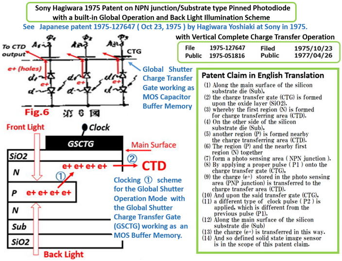
The Japanese Patent ( 1975-127647) shown below is
the evidence that Hagiwara at Sony is the inventor of
the Pinned Photo Diode with the Back Light Illumination.
The details are explained below.
The details of the Japanses Patent Claim
( JAP 1975-127647 )
by Yoshiaki Hagiwara at Sony in 1975.
Patent Clamis in Japanese
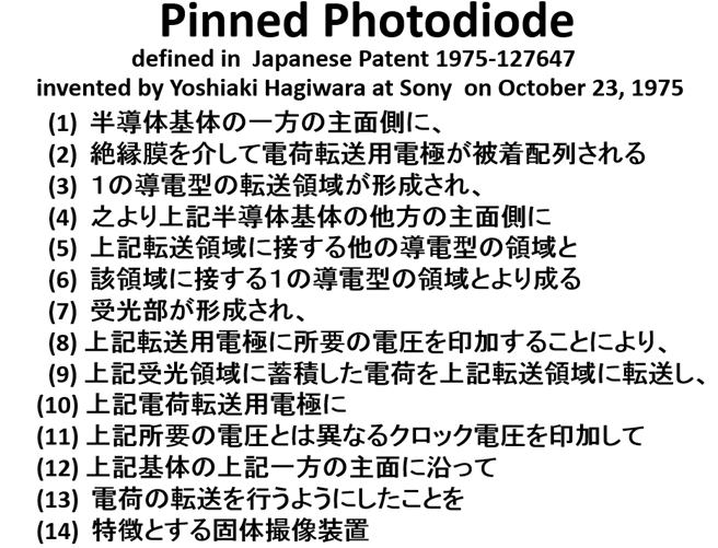
Each Step (1) thru (14) of the Patent Claims
is explained below with English translation.
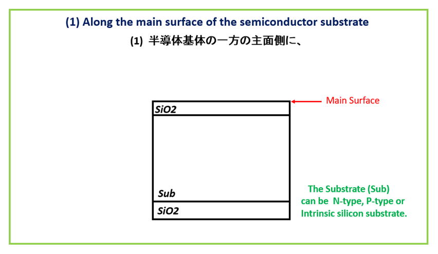
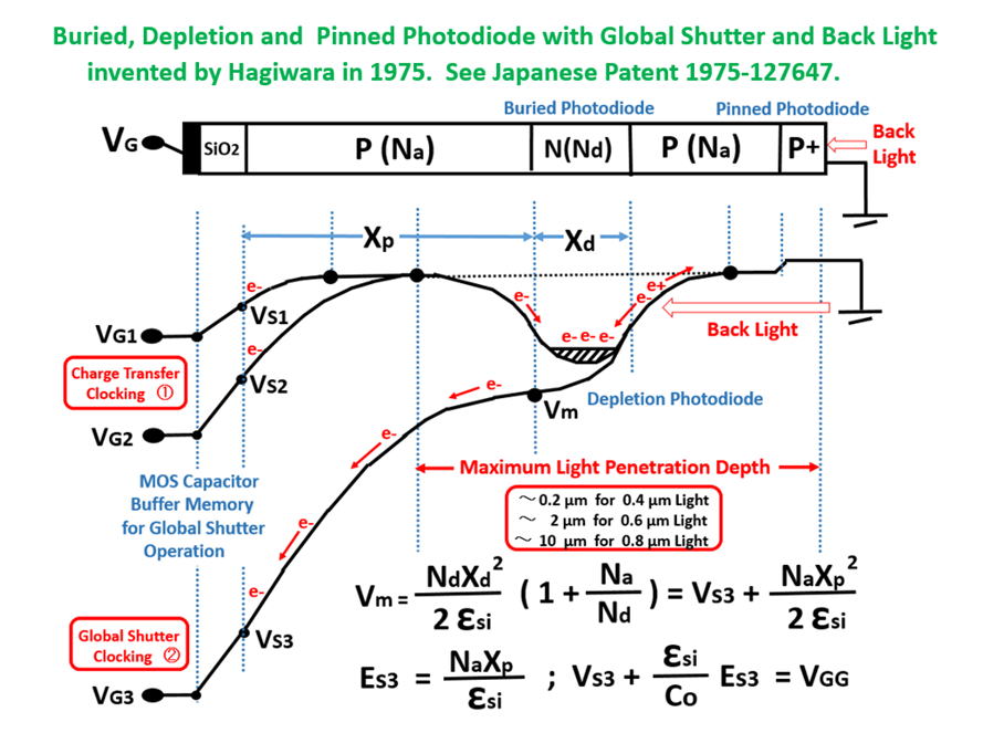
The substrate must have thined but kept to
more than about the thickness of 10 um in
order to block the back light penetrating
thru the silicon crystal from the back side
of the silicon wafer. The silicon wafer must
be by necessity a lightly doped N type or
a P type wafer or an intrinsic wafer to have
enough extention depth of the depletion
region for charge collection and charge
transfer operation.
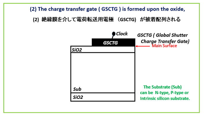
Since the substrate is thined but kept to
more than about the thickness of 10 um,
the back light penetrating thru the silicon
crystal from the back side of the silicon
wafer can be blocked from reaching the
surface region under the charge transfer
gate in the Global Shutter Operation.
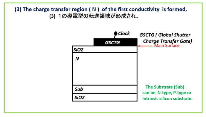
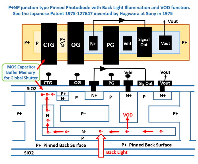
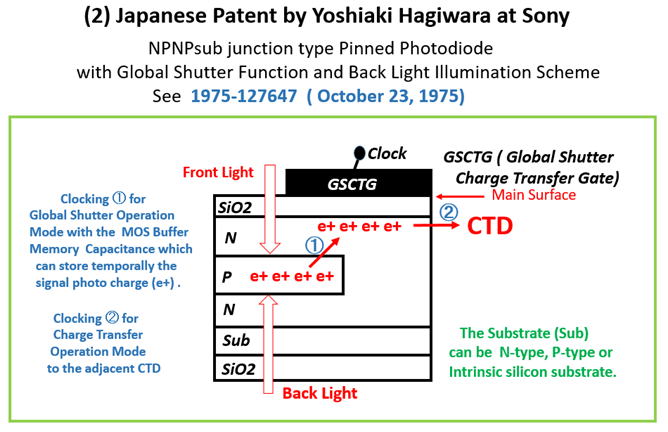
The first conductivity region could be
an N-type well with a lightly doped
N-type substrate wafer for simplicity.
In this case we would have the hole (e+) signal charge and
the buried P+ type charge collection region for simplicity.
To have the vertical overflow drain (VOD) function, however,
the first conductivity type could be N type well with the P type
substrate wafer.
In this case we would also have the hole (e+) signal charge and
the buried P+ type charge collection region. Then, the signal
chare hole (e+) can be drained to the P type substrate region
that acts also as the drain of the vertical overfow drain (VOD) .
In either case, the substrate voltage potential must be fixed or
pinned to a positive supply voltage for the N type substrate or
to the ground voltage for the P type substrate wafer.
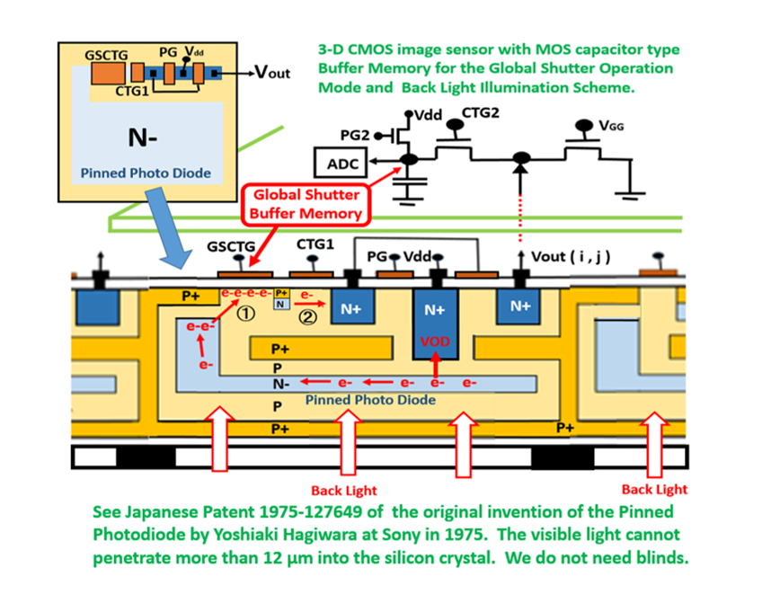
The patent claimed device structure is a Pinned Photodiode
with the built-in overflow drain (VOD) function and also with
the Back Light Illumination Scheme.
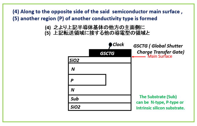
In either case, the substrate wafer ( P type for example ) and
the first conductivity region ( N type well for example ) must
be both lightly doped for the Back Light Illlumination case.
And for the case of the Front Light Illumination,
similar to the conventional Interline Transfer
CCD image sensor, the charge transfer gate
must be shielded by metal to block the front light.
illumination.
But by forming the buried P layer deep enough
in the silicon wafer of about 3 um depth.
As can be easily undersood, this dvice is a Buried
photodiode structure. But this is a partially Pinned
Photodiode since the frond surface side of the
SiO2 exposed window is not really pinned.
This is the reason why a Buried Photodiode is not
necessarily a Pinned Photodiode if the charge
collection region is close to the SiO2 exposed
silicon wafer.
However Hagiwara invention of the Buired Photodiode
is clearly intended to have the Buried Photodiode
being buried deeply in the silicon wafer depth of about
3 um depth range in mind in the practical applications.
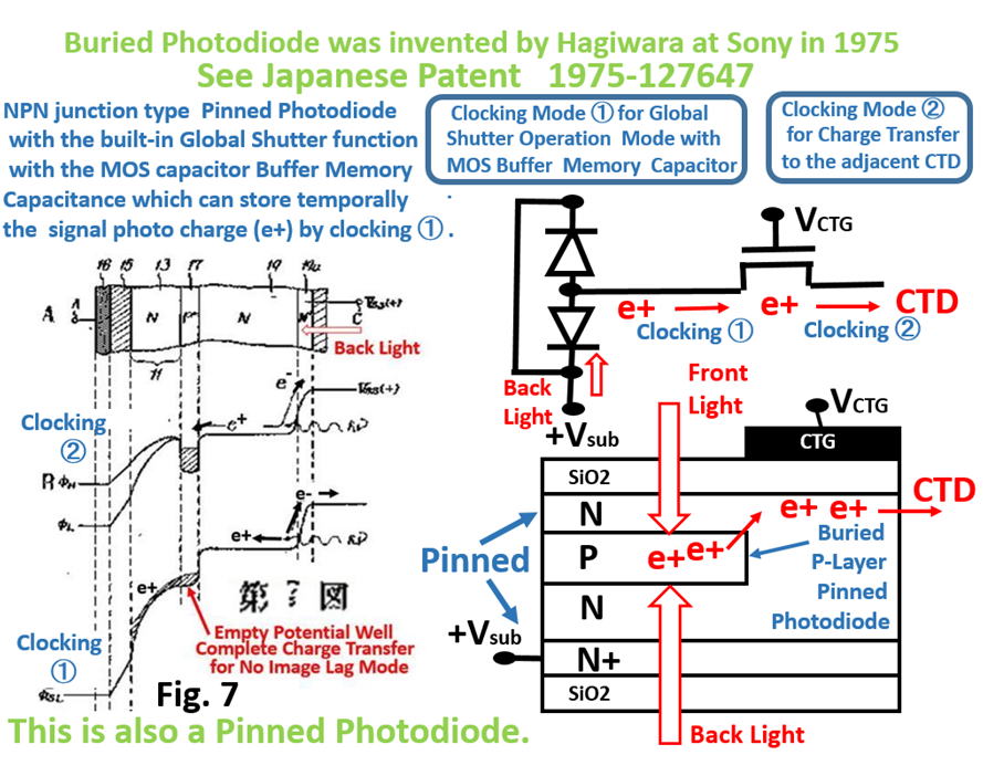
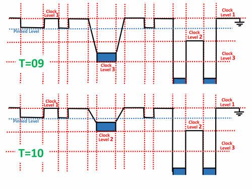
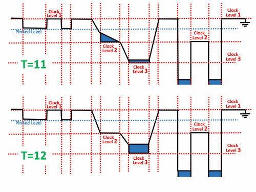
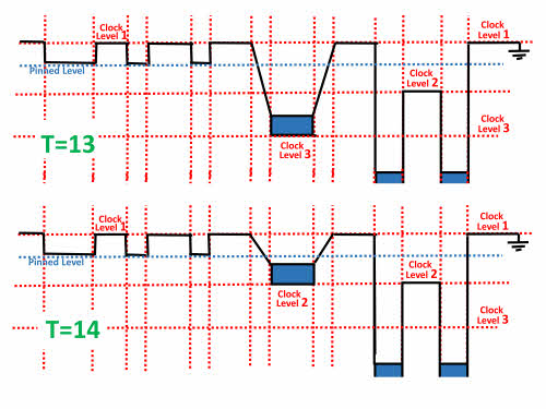
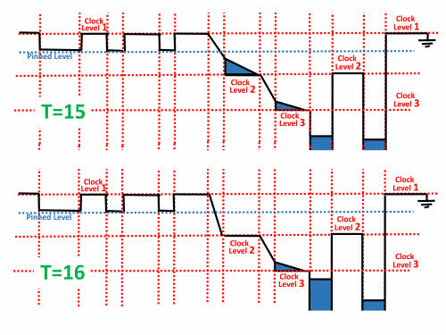
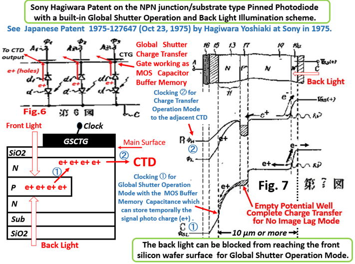
These important observations can be easily perfomed
thru the figure 7 of the patent application example.
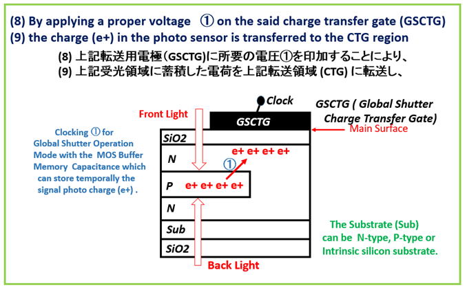
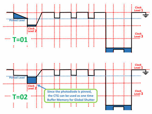
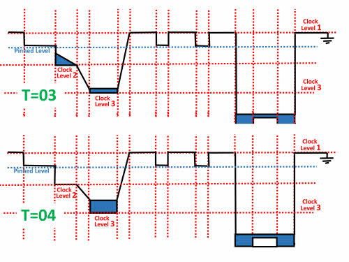
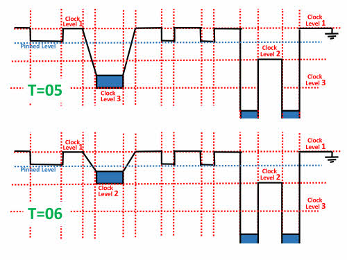
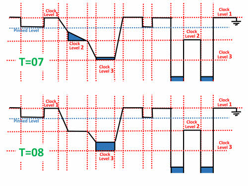
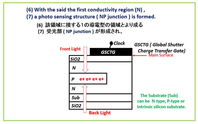
At this point, the charge is stored at the surface of the charge
transfer gate which works as the MOS capacitor type Buffer
Memory for the Global Shutter Operation Scheme. The back
light cannot reach more than 10 um depth of silicon crystal.
Hence in case of Back Light Illumination, the charge transfer
gate acts as the Global Shutter Charge Transfer Gate (GSCTG).
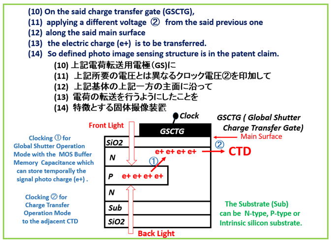
Then the charge under the Global Shutter Charge Tansfer
Gate (GSCTG) is transfered to the adjacent Charge Transfer
Device (CTD) which can be either CCD type CTD or CMOS
type CTD. In case of CMOS type CTD, for Global Shutter
Operation Scheme, a buffer memory is always needed, that
can be a MOS capacitance type buffer memory as in this
patent claim or a NP junction capacitance type bufffer
memory that can be easily considered as an alternative
buffer memory for the Global Buffer Operation. Either way,
Hagiwara invented the Pinned Photodiode with the Back
Light Illumination and the Global Shutter Operation
Scheme as decribed in the figure .7 of the application
example of the 1975-127647 Japanese Patent as
shown below. The backside of the silicon wafer is
clearly shown being pinned by the substrate metal
contact with the heavily doped N+ region, which is
the evidence that Hagiwara invented the Pinned
Photodiode with the completely depleted charge
collection region (p+) of the buried photodiode.
It is easily understood that the silicon substrate,
shown in the Figure 7 below, must be a lightly
dope N-type substrate for the Back Light
Illunination Shceme.
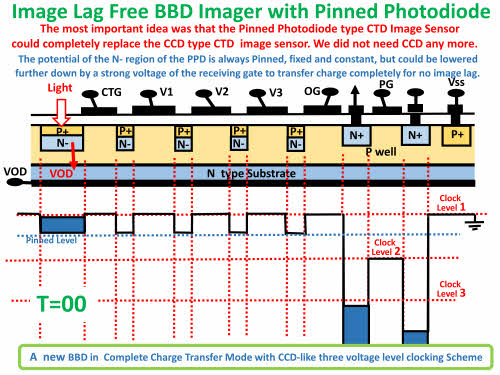
Today CMOS image sensor is prevailing, and
the in-pixel buffer memory for the Global
Shutter Operation is a must.
Hagiwara in 1975 invented the the in-pixel
buffer memory for the Global Shutter Operation
of the Back Light Illlumiantion type Pinned
Photodiode that opened the gate for the
multi-functionality of CMOS Image sensors.
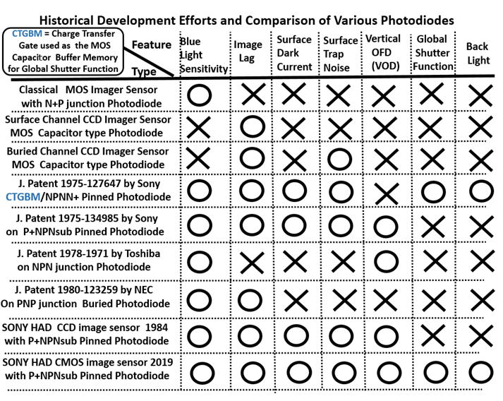
CCD was the Super Star because the global shutter function
can also be buitt-in while the conventional MOS image sensor
needed an extra N+Psub diffusion type buffer memory capacitance
which we could not afford to include in each small pixel.
The first generation image sensor engineers all knew about this fact.
It was considered as a weak feature of the MOS image sensor.
The MOS image sensor needed the extra buffer memory in order
to perform the golabl shutter function while the CCD image
sensor can easily perform the global shutter function without any
extra buffer memory because the CCD itself is composed of memory
capacitor arrays.
The global shutter scheme was a common understanding after CCD
was invented. And no one tried to file a patent on this common
knowledge on the MOS image sensor until more than 20 years later
the CMOS process technology gets so advanced that each MOS image
sensor pixcel can afford to include the active source follower circuit
and the buffer memory for the global shutter function.
************************************************
*************************************************
The AIPS image sensor watching at its inventor, Yoshiaki Hagiwara.
return to http://www.aiplab.com/TOP Page