**********************
The AIPS ( Artificial Intelligent Partner System ) Home Page 042
hagiwara-yoshiaki@aiplab.com
Private Communications with Prof. Albert Theuwissen
**********************
Yoshiaki Hagiwara is the inventor of SONY original HAD sensor.
SONY HAD is defined as the P+/N/Pwell/Nsub junction type
thyristor photo sensing structure, originally invented by Yoshiaki
Hagiwara at SONY in 1975. See the 1975-134985 Japan Patent.
SONY HAD sensor (HAD1975) is identical to the P+NP junction
type Pinned Photodiode (PPD1980) with the NPNsub junction
type built-in Vertical Overflow Drain (VOD1978) Photodiode.
PPD1980 and VOD1978 are derivative of the Hagiwara 1975
invention of HAD1975 which is SONY original HAD sensor. .
Consequently Hagiwara (HAD1975) at SONY is the original and
true inventor of the Pinned Photodiode (PPD1980) and the
in-pixel built-in Vertical Overflow Drain Photodiode (VOD1978).
**********************
Pinned Photo Diode Patent invented by Hagiwara in 1975
Story of Pinned Photo Diode (html)
Hagiwara at SONY is the true inventor of Pinned Photo Diode (html)
See also ElectronicsStackExchangeSite on "What is Pinned Photo Diode ? "
Pinned Photo Diode was invented by Hagiwara of Sony in 1975 (PDF)
Hagiwara at Sony invented Pinned Photo Diode in 1975(PDF)
****************************************************
Please read the narratives about the CCD inventors.
https://www.dpreview.com/articles/3397331369/nobelprize
This artical says, "The CCD technology makes use of the
photoelectric effect, as theorized by Albert Einstein and
for which he was awarded the 1921 year's Nobel Prize.
By this effect, light is transformed into electric signals.
The challenge when designing an image sensor was to gather
and read out the signals in a large number of image points,
pixels, in a short time."
This statement is partly correct, but not exactly correct.
The device which transforms light into electric signals
is called as the photo sensor.
The device which gathers and reads out the electric signals
in a large number of image points, pixels, in a short time
is called as the charge transfer device(CTD).
CCD can act both as the photo sensing device and the
charge transfer device(CTD) and was the Super Star.
But the CCD type photo sensor was replaced by the
Pinned Photodiode developed by Sony in 1978, which
was based on Hagiwara 1975 invention of the P+NPNsub
junction type Pinned Photodiode with the vertical
overflow drain. Later NEC also replaced the CCD type
photo sensor by developping the P+NP junction
type Pinned Photodiode, which is identical to the
Hagiwara 1975 invention of the P+NPNsub junction
type Pinned Photo Diode.
SONY and NEC gave up already in early 1980s using
the CCD type photo sensor, and instead, used the
Pinned Photodiode which is highly-light-sensitive,
low-dark-current and low-image-lag, much better
than the CCD type photo sensor.
In1984 SONY successfully developped the SONY
original Hole Accumulation Diode (HAD) which is
the P+NPNsub junction type photo sensor, which
is Hagiwara 1975 invention.
As well known , the P+NPNsub junction is a thyristor
type structure , which is composed of two junction
type transistors.
One is the top part of the P+NPNsub junction,
which is the P+NP junction type photo diode, now
called also as the Pinned Photo Diode.
Hence, the Pinned Photo Diode is also included in
the Hagiwara 1975 invention of the P+NPNsub
junction type photo diode.
The other one is the bottom of the P+NPNsub junction,
which is the NPNsub junction type photo diode acting
as the vertical overflow drain (VOD) which was invented
independently by Yamada at Toshiba in 1978.
But Hagiwara 1975 invention is earlier than Yamada
1978 invention and Teranishi 1980 invention. Both
Yamada 1978 invention and Teranishi 1980 invention
are not valid. They are duplicated copies of Hagiwara
1975 invention of the P+NPNsub junction type photo
sensing structure, which is now called as SONY HAD.
CCD is one type of CTD. Before CCD, MOS type CTD was
known. Now, CCD type CTD are completely replaced by
CMOS type CTD completely. Why ???
CCD is made of many MOS capacitors. The MOS capacitor
has the metal electrode. Metal type electrodes including
polysilicon electrodes are highly conductive with many
moving-electron charges that interact with, and reflect, light.
Metal does not let light pass thru the metalic electrodes.
Therefore CCD itself no way can become a good light
detecting photo sensor.
Hagiwara at SONY in 1975 invented the SONY HAD
sensor, which has a highly-light-sensitive, no-image-lag,
no-dark-currentand no-trap-noise photo sesnor structure
of theP+NPNsub junction type Pinned Photodiode with
the vertical over flow drain (VOD) structure.
See Japanese Patent 1975-134985.
Now, the CCD type CTD image sensors are completely
taken over by the CMOS type CTD imagers.
Now the CCD type CTD image sensors completely
disappeared from the image sensor world. Why ???
SONY and many other companies are not producing
CCD type CTD image sensors any longer. Why ????
TheCCD type CTD image sensor was the Super Star
during 1980s and 1990s. But now the CMOS type CTD
imager sensor is the Super Star. Why ??
Remember ?
A solid state image sensor has two important parts.
One is the light detecting structure that makes use
of the photoelectric effect, as theorized by Albert
Einstein and for which he was awarded the 1921
year's Nobel Prize.
By this photo-electron effect, light is transformed
into electric signals.
However, this CCD-type light detecting sturcture
was no longer used since early 1980s because SONY,
NEC and other companies replaced it with another
type of light detecting sturcture.
This CCD-type light detecting sturcture had many
disadvantages and poor performance.
The new photo sensing structure is now called as
the SONY original HAD ( hole accumualtion diode )
invented by Hagiwara at SONY in 1975, which is the
Pinned Photodiode with the in-pixel vertical overflow
drain (VOD) structure.
The other is the charge transfer device(CTD) that
was a big challenge when designing an image sensor
in order to gather and read out the signals in a large
number of image points, pixels, in a short time.
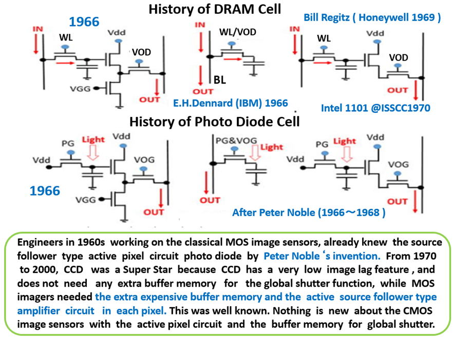
Historically we had a classical MOS type CTD without
in-pixel active curicuits until in 1966 Peter Nobel
invented the in-pixel active curicuits. However,
CMOS process technology was not well advanced.
Then, the CCD type CTD became the Super Star
as you know well. But after 50 years the CMOS
scale-down technology became well advanced.
We now can put the in-pixel active curicuits
invented by Peter Nobel in 1966 in each image
sensor picture element cell area.
And now the CCD type CTD image sensors were
completely replaced by the CMOS type CTD image
sensors. We no longer need the CCD type CTD
image sensors. We no longer need CCD completely.
However since Sony 1978 publication of the Pinned
Photodiode, we use still now the same light detecting
structure of the P+NPNsub junction type photodiode
that makes use of the photoelectric effect, as theorized
by Albert Einstein and for which he was awarded the
1921 year's Nobel Prize. By this photo-electron effect,
light is transformed into electric signals.
This light detecting sturcture is the SONY original
HAD(hole accumualtion diode) invented by Hagiwara
at SONY in 1975, which is the Pinned Photodiode with
the in-pixel vertical overflow drain (VOD) structure.
Hagiwara 1975 invention of the P+NPNsub junction type
photodiode makes use of the photoelectric effect, as
theorized by Albert Einstein and for which Albert Einstein
was awarded the 1921 year's Nobel Prize.
By this effect, light is transformed into electric signals.
This function was NOT performed by CCD at all since 1978,
because the CCD type photo sensor structure had many
disadvantages.
But the world called this image sensor with the Pinned
Photodiode sensor and the CCD type CTD, for a long
time, as a CCD image sesnor.
Now the world calls the image sensor with the Pinned
Photodiode sensor and the CMOS type CTD, for a long
time, as a CMOS image sesnor.
The world is completely ignoring the most important
lihgt-detencting sensor strucutre of the Hagiwara
1975 invention of the P+NPNsub junction type SONY
HAD sensor, which is the combination of the P+NP
junction type Pinned Photodiode and the NPNsub
junction type vertical overflow drain(VOD).
Hagiwara 1975 invention of the P+NPNsub junction type
photodiode was used since 1978 on, is being used till now
and will be used in future definitely, to transform light into
electric signals efectively, making use of the photoelectric
effect, as theorized by Albert Einstein and for which Albert
Einstein was awarded the 1921 year's Nobel Prize.
That is, CCD was NOT used as the device to transform light
into electric signals any longer in practical image sensor
applications in world wide, after the Hagiwara 1975 invention
of the P+NPNsub junction type photodiode, which is now called
as the Pinned Pinned Photo or by another name of the SONY
original HAD ( Hole AccumulationDiode).
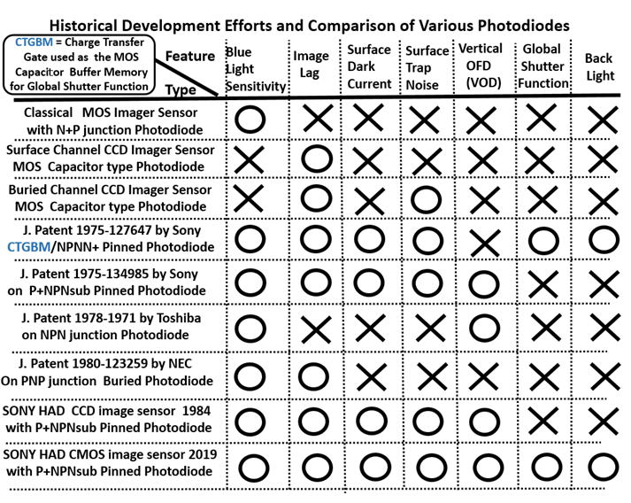
The reasons are shown clearly in the above table. The CCD type
photo sensor structure had many disadvantages as shown above
table. The world gave up using CCD for the Pinned Photo Diode
as the light detecting photo sensor structure when SONY held
the Tokyo and New York Press Conference in 1978, where SONY,
for the first time in the world, published a low image lag, low
dark current, low trap noise , but highly light sensitive Pinned
Photodiode in the CCD type charge transfer device(CTD).
The challenge when designing an image sensor was to gather
and read out the signals in a large number of image points,
pixels, in a short time. For this purpose as a charge transfer
device(CTD), the buried channel CCD was the Super Star
since its charge transfer efficiency is close to 99.999% while
the surface channel CCD had only charge transfer efficiency
of 99.9 % was completely useless in 1970s.
Nowadays, the charge transfer efficiency of 99.999% of the
buried channel CCD also became completely useless for high
definition high resolution 8K and16K digital televion picture
qualities. Beside, CCD tyep CTD consumes a lot of power.
However, the Hagiwara 1975 invention of the Pinned Photo
Diode with the vertical Overflow Drain (VOD) function is
still valid and useful in the Modern CMOS type CTD image
sensors, which now have in-pixel active source follower
current amplifier circuits that was originally invented by
Peter Nobel in 1966. So CCD became completely useless.
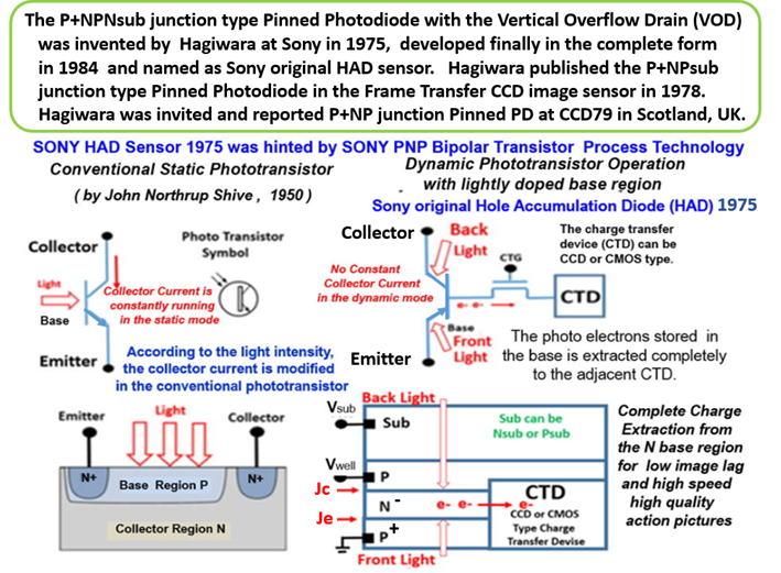
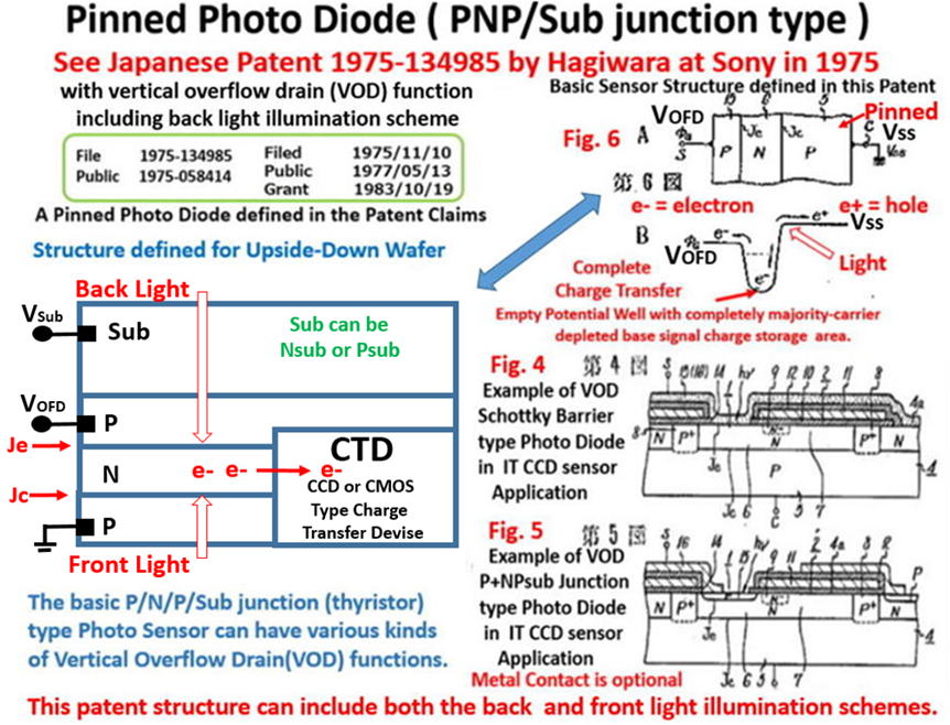
Hagiwara invented, in his 1975 Japanese Patent 1975-134985,
the P+NPNsub junction type photodiode structure, which is
the origin of all the modern highly light-sensitive, low-noise,
low-dark current and low image-lag pinned photodiode with
the vertical overflow drain(VOD) structure.
This photo sensor was later in 1984 called as the SONY
original HAD ( Hole Accumulation Diode ) sensor right after
SONY successfully developed the mass production process
technology of this P+NPNsub junction type photodiode
structure for the first time in the world.
SONY took more than 9 years after the Hagiwara 1975 invention
simply because the P+NPNsub junction type photo diode needed
a very complex process technology which is the combination of
the classical bipolar process technology and the MOS process
technology dedicated to realize the CCD image sensor process.
However, SONY developed the P+NPsub junction type Pinned
Photo Diode without VOD for the first time in the world in 1978,
which is just an upper part of the Hagiwara 1975 invention of
the P+NPNsub junction type, which is a combined structure of
the P+NP junction type Pinned Photodiode with the NPNsub
junction type Vertical Overflow Drain (VOD) function structure.
In 1978, SONY published a FT CCD image sensor with the
P+NPsub junction type Photodiode which is now known as
the Pinned Photo Diode. It was the first publication of the
SONY HAD sensor, but it did not have the vertical overflow
drain (VOD) structure. Instead, a conventional lateral overflow
drain (OFD) was applied for this SONY HAD FT CCD image
sensor with the P+NPsub junction type Photodiode, which
is also now widely known as the Pinned Photo Diode.
Later in 1978, independently Yamada at Toshiba invented the
NPNsub photodiode with the vertical overflow (VOD) structure.
This is just the lower part of the Hagiwara 1975 invention of
the P+NPNsub junction type photo diode, which is a combined
structure of the P+NP junction type Pinned Photodiode with the
NPNsub junction type Vertical Overflow Drain (VOD) function.
So the VOD structure invented by Yamada at Toshiba in 1978
is a duplicatied copy of Hagiwara 1975 invention explained above.
Later in 1980, independently Teranishi at NEC invented the
P+NPsub junction type ( Buried layer ) Pinned Photodiode
But this is just the upper part of the Hagiwara 1975 invention of
the P+NPNsub junction type Pinned Photodiode which is a
combination of the P+NP junction type Pinned Photo Diode(PPD)
and the NPNsub junction type vertical overflow (VOD) structure.
So the VOD structure invented by Yamada at Toshiba in 1978
is a duplicatied copy of Hagiwara 1975 invention explained above.
Teranish at NEC published the no image lag ILT CCD image
sensor with the buried photo diode in IEDM1983.
However, SONY already published no image lag ILT CCD image
sensor in 1978 with the transparent electrode and lateral
overflow drain. SONY also developed and published the no image
lag FT CCD image sensor in 1978 with the Pinned Photo Diode
and with the lateral overflow drain.
Finally SONY developped SONY original HAD sensor in 1984,
which is a combination of the Pinned Photo Diode(PPD)
with the vertical overflow (VOD) structure for the first time.
in the world.
This combined structure of the PPD and VOD, is now known
as the SONY original HAD sensor, which is the Hagiwara 1975
invention, defined in Hagiwara Japanese Patent 1975-134985.
So it can be concluded that the Pinned Photodiode was invented
by Yoshiaki Hagiwara at SONY in 1975. Teranishi did not.
It can also be concluded that the vertical overflow drain(VOD) was
invented by Yoshiaki Hagiwara at SONY in 1975. Yamada did not.
To study and learn more about image sensors updated,
visit http://image-sensors-world.blogspot.com/
Here is a story of the world efforts
on early image sensor developments.
Original Photodiode and Phototransistor was invented
by John Northrup Shive in 1950 right after the invention
of bipolar transistor in 1947.
Invention History of Phototransistor and Photodiode
I am completely retired and no longer any expert.
But, once again, I am now trying to review and study
the image sensor world efforts.
(1) who is the original and true inventor of the Pinned Photodiode ?
(2) who is the one with the most significant contributions on
the CMOS type charge transfer devices (CTD) ?
As you know an image sensor is composed of two important parts.
One is the photo diode and the other is the charge transfer device(CTD).
The CCD type CTD was the Super Star but we no longer need it.
The CMOS type CTD is now working well with in-pixel amplifier circuits.
There are many quotations and narratives on Fossum and Teranish.
But I do not believe that Fossum is the major contributor of CMOS
Image sensor developments. I do not believe that Teranish is the
original inventor of the Pinned Photo Diode.
The following is my point of views on image sensor developments.
Original Photodiode and Phototransistor was invented
by John Northrup Shive in 1950 right after the invention
of bipolar transistor in 1947 as you know well.
Hagiwara was born on July 4, 1948 in Kyoto, Japan.
So, Hagiwara was maybe a single egg during the 1947
Christmas season when the transistor was invented.
Hagiwara left Japan in 1965 to live in Riverside, California
at age 17. Hagiwara was just a young high school student
at Riverside Polytechnic High School, very much interested
in science and technology, when Peter Noble invented
the in-pixel amplifiers in 1966.
Hagiwara moved to Pasadena, which is only 60 miles away
from Riverside, to study as an undergraduate student at
California Institute of Technology (Caltech) in Sept, 1967.
While Hagiwara was just a college student at Caltech, more
details were disclosed about image sensor elements with the
in-pixel amplifiers and were more intensively described by
Noble, and later by Chamberlain and by Weimer et al. in 1969.
At that time, passive-pixel sensors – that is, pixel sensors
without their own amplifiers or active noise cancelling
circuitry – were being investigated as a solid-state
alternative to vacuum-tube imaging devices.
Hagiwara was just a college student interested in
photo-transistors, while studying Feynman Physics
and the physics of semiconductor by Andy Grove.
Then, CCD was invented and became soon the Super Star
because CCD has the global shutter function and no image
lag features that can be applied to realize fast action motion
pictures while the MOS type charge transfer device (CTD)
needs an in-pixel extra buffer memory which was very
expensive to be included in each pixel.
In late 1990s, engineers in JPL at Caltech reported
the global shutter scheme for MOS image sensor
using the extra buffer memory in each pixel. But
the global shutter scheme was not their invention.
The pioneering image sensor engineers in 1970s all
knew the built-in global l shutter function of the CCD
Super Star in 1970s. They all knew that CCD did
not need the extra expensive in-pixel buffer memory
while the conventional MOS image sensors needed one.
Hagiwara was a visiting professor of EE and Applied
Physics departments at Caltech. Hagiwara visited
often JPL and had frequent communications with
Dr. Pain's team of MOS image sensor working group.
They were not happy about Fossum's fraud actions.
Hagiwara did not understand the details.
But later Fossum published a 2013 fake paper
attacking Hagiwara 1975 patent by claiming that
Hagiwara 1975 PNP junction photo diode did not
have the complete charge transfer operation feature,
which was not true. And Fossum misled the world.
Hagiwara is finally convinced that Fossum is a fraud.
In late 1990s, as we all expected, CMOS scaled down
technology became so advanced, it became possible
to realize image sensor elements with in-pixel
amplifiers invented by Nobel. We all knew the trend.
This is not Fossum's idea. Fossum did nothing.
CCD type CTD image sensors are now completely
taken over by CMOS type CTD image sensors.
The CCD charge transfer efficiency of 99.999 % is
no longer enough to achieve the high definition
digital TV picture quality. CCD became useless.
It is well known that an image sensor is composed of
two important devices, one is the charge transfer
device (CTD) as described above, and the other is
the light detecting, photo sensing semiconductor device.
Especially, the light detecting, photo sensing structure
must be highly light sensitive, low trap noise, low dark
current and low image lag features with the high light
protection (VOD) capability.
This light detecting, photo sensing device structure
was invented by Hagiwara at SONY in 1975 in the form
of P+NPNsub junction type photo thyristor structure.
See JAP 1975-134985.
The P+NPNsub junction type photo thyristor structure
Hagiwara at Sony invented in 1975 has the hole accumulation
Pinned P+ layer on the top of the P+NPNsub junction.
This was the origin of SONY HAD( Hole Accumulation Diode)
developed by SONY in 1984.
Besides, as Hagiwara explained in the patent, as an
application example, this P+NPNsub junction structure
has inherently the built-in capability of vertical overflow
drain (VOD) capability.
It is well known that the P+NPNsub junction type photo
thyristor structure is composed of two junction bipolar
transistor structures.
One is the P+NP junction type photo transistor structure
and the other one is the NPNsub junction type photo
transistor structure.
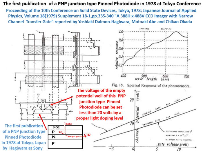
In 1978 Hagiwara at SONY published the one chip color
FT CCD CTD type image sensor with the P+NP junction
type photo transistor structure, which later was cited as
the first publication of the Pinned Photo Diode by Prof.
Albert Theuwissen in his many technical presentations.
In 1978 Yamada at Toshiba filed a patent on the NPNsub
junction type photo transistor structure with the vertical
overflow drain (VOD) function. This structure is included
in the Hagiwara 1975 invention above.
In 1980 Teranishi at NEC filed a patent on the PNP
junction type photo transistor structure with the
buried N layer. But this PNP structure is included
in the Hagiwara 1975 invention above.
In 1983, Teranishi et al at NEC published the one chip color
ILT CCD CTD type image sensor with the P+NP junction
type photo transistor structure at IEDM1983. But no one
seemed to know that this PNP structure had been already
defined in the Hagiwara 1975 invention explained above.
At that time, SONY was working for the P+NPNsub junction
type photo diode of Hagiwara 1975 invention. In 1984, SONY
successfully developed the SONY original Hole Accumulation
Diode (SONY HAD) with the vertical overflow drain (VOD)
structure as originally defined in Hagiwara 1975 invention.
The world misunderstood that SONY developed SONY HAD
in 1984 following after Yamada 1978 invention and Teranish
1980 invention. But the truth is that SONY developed SONY
HAD in 1984 following after Hagiwara 1975 invention.
That is the reason why SONY called SONY Original HAD.
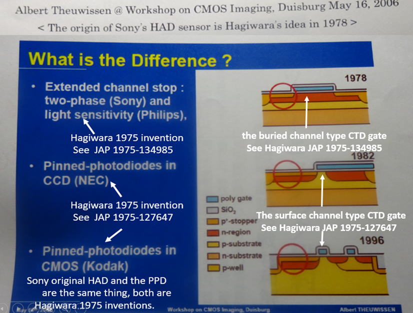
Prof. Kagami of Tohoku university. pointed out in his technical
presentations that SONY HAD and Pinned Photodiode
are identical, the same thing that has two names.
At that time, SONY was the only company in the world
that had the mass production process line and technology
of the complex P+NPNsub junction type photo sensor.
SONY called the technology SONY HAD, but it was the
Hagiwara 1975 invention, which is the combination of
Teranishi 1980 invention of the Pinned Photo diode and
Yamada 1978 invention of the vertical overflow drain(VOD).
Now, it should be conclude that Teranishi 1980 invention
of the Pinned Photo diode is a copy of Hagiwara 1975
invention and also that Yamada 1978 invention of the
vertical overflow drain(VOD) is a copy of Hagiwara 1975
invention. Teranishi 1980 invention and Yamada 1978
invention must be copies, duplications or derivatives of
Hagiwara 1975 invention.
CCD image sensor mass production was possibile for
SONY because SONY already had the bipolar mass
process technology needed for signal processing bipolar
LSIs for SONY color home video and television sets.
NEC could not establish the mass production process
line and technology of the complex P+NPNsub junction
type photo sensor. Eventually, NEC gave up making CCD
image business while Panasonic never give up. Later
many companies were encouraged by SONY's success
and followed Sony. But remember that Sony image
sensor efforts exploded by Hagiwara 1975 invention.
Hagiwara at age 26 was the single engineer and scientist
designing and testing alone the image sensors in Sony.
He also had to develop in-house CCD design CAD tools
in a very small resrerch team working at Sony Yokohama
Resarch Center under the leadership of Sony President,
Iwama Kazuo, a bipolar transistor device physicist at Sony.
.
****************************************************
Private Communications with Prof. Albert Theuwissen
on the invention of Pinned Photo Diode (PPD)
Also see Prof. Albert Theuwissen's blog.
****************************************************
Conclusions:
Peter Noble invented the in-pixel active source-follower
type current amplifier circuit. Fossum did not invent it.
Yoshiaki hagiwara invented the Pinned Photo Diode with
the vertical OFD function. Teranish did not invent it.
Fossum and Teranish are incorrectly attributed to the modern
CMOS image sensor invention and development efforts.
****************************************************
Hi Yoshi,
I do agree with you that the structure
you invented in 1975 and developed in 1978
is indeed a PPD, maybe not called that way
at that time and also invented for some other
purpose ( such as VOD).
But it still remains a PPD !
At Philips, in the late '70s a very similar structure
was implemented in the CCDs, this was before
I joined Philips in 1983.
So yes, there were several p+/n-/p- structures known
by the time that Teranishi issued his 1980 patent .
I fully agree to that.
Looking forward to hear from you,
****************************************************
> FROM: hagiwara [mailto:hagiwara-yoshiaki@aiplab.com]
> SENT: Tuesday, July 10, 2018 3:19 PM
> TO: 'a.theuwissen'
> SUBJECT: RE: NEC-SONY Patent War
>
> Hi, Albert,
>
> how are you ?
>
> I am very mad at Fossum's 2014 paper
>
> which I found just a few weeks ago.
>
> I am now 70 years and completely retired..
>
> Fossum did not quote the very important
>
> Pain's work at JPL CalTech
>
>on theGlobal Shutter CMOS image sensor ...
>
> Yoshi
**************************************************
On Tue, 10 Jul 2018 18:24:23 +0900, hagiwara wrote:
> Albert,
>
> I am sorry my previous e-mail title was in Japanese,
>
> copying to many unrelated people.
>
> But they are also my friends.
>
> I am re-sending with more information
> on the Pain's paper.
>
> You know, I was also a visiting professor
> at CalTech during 1998 to 1999
>
> and frequently visiting Pain's Lab at JPL,
> CalTech during the period.
>
> I remember Pain and his team really hated
> Fossum at that time.
>
> I recall they called Fossum a thief.
>
> Kind regards
>
> Yoshi
>
***************************************************
From: albert theuwissen
Sent: Tuesday, July 10, 2018 6:55 PM
To: hagiwara-yoshiaki@aiplab.com
Subject:
Re: How are you ? from Yoshi of Sony(Hagiwara180710)
Dear Yoshi,
Good to hear from you, although it is not all good news
you are sending to me.
Can you tell me the reference of the Pain paper ?
When and where was it published ?
Very interesting information !!
At the time Fossum started to write the overview paper
about the PPD, he asked me to become a co-author
and to help him out with the paper.
After some doubt I declined his invitation,
because I do know that the discussion
about the inventor of the PPD is very sensitive,
and I do agree with you that the structure
you developed is indeed a PPD,
maybe not called that way at that time and
also invented for some other purpose.
But it still remains a PPD !
At Philips, in the late '70s a very similar structure
was implemented in the CCDs, this was before
I joined Philips in 1983.
So yes, there were several p+/n-/p- structures
known by the time that Teranishi issued his patent.
I fully agree to that.
Looking forward to hear from you,
Regards,
Albert.
***************************************************
***************************************************
From: Albert Theuwissen
Sent: Thursday, November 22, 2018 5:48 PM
To: hagiwara-yoshiaki@aiplab.com
Subject: Fwd: I just visited SONYKumamoto Tech Center
Dear Yoshi,
Thanks for your mail.
I remember the discussion during IISW2013
when Mike Tompsett gave a keynote speech.
He owns the patent entitled "Charge-Couple Device Image
Sensor", while his 2 colleagues Boyle and Smith received
in 2009 the Nobel Prize for the invention of the CCD Image
Sensor.
Very much in contradiction, but unfortunately
that is sometimes the way things happen.
What we also very often see is that a major invention is
based on other things that happened around the inventor.
Sometimes the inventor is triggered
by work of others in the same field.
The only advice I can give you :
do not put too much energy in this,
you cannot change history and
it only makes your frustration bigger.
But if I give talks and trainings about image sensors,
including the working principle of PPD,
I ALWAYS refer to (1) your work,
(2) Philips' work (which is more or less a copy of
what you did, but 1 or 2 years later than yours) and
(3) Teranishi's work.
So I do not forget you !!!
I think that the active pixel sensor
with an in-pixel source follower
is described for the first time
by Peter Noble, in 1968
or maybe already in 1966.
He just published a book about his invention.
BTW, I am a bit jaelous on you
because you had the opportunity
to visit the fab of Sony in Kumamoto.
This is one of my dreams
to ever visit the Sony's fab,
including their test facilities.
Wishing you all the best in everything you do !!
Regards,
Albert.
**********************************************************
From: Albert Theuwissen
Sent: Tuesday, November 27, 2018 1:35 AM
To: hagiwara-yoshiaki@aiplab.com
Subject:
RE: the Japanese Official Invention WEB site
Hi Yoshi,
It is everywhere the same story.
What do you think :
- who invented/developed the stitching technology
for large area image sensors ?
- who owns the world record in low-noise
in the voltage domain for CIS ?
Regards, Albert.
*******************************************************
From: hagiwara [mailto:hagiwara-yoshiaki@aiplab.com]
Sent: Wednesday, February 20, 2019 12:36 PM
To: 'Albert Theuwissen'
Subject:
RE: Please copy to Dr.Nakamura and Dr.Pain
RE: I actually filed in 1975 three Japanese patents (Hagiwara181212)
Hi, Albert,
Thank you very much for Nakamura-san's e-mail.
I mailed Nakamura-san and he seemed a bit confused ??
I am now explaining Nakamura-san that
In 1975, Hagiwara invented
a P+NPNsub junction type photo-diode,
which is now called in Sony internally
the SONY original HAD sensor.
In 1980, Teranishi-san invented
a P+NPsub junction type buried photo diode
which is identical to the P+NP junction of
the P+NPNsub junction type photo diode
defined as the SONY original HAD sensor.
In 1978, Yamada-san invented
a NPNsub junction type photo diode
with vertical OFD (VOD) function,
which is not a PPD but with VOD,
but identical to the NPNsub junction of
the P+NPNsub junction type photo diode
defined as the SONY original HAD sensor.
The charge is stored in the N region and
to be transferred to the adjacent charge
transfer device with the complete charge
transfer mode resulting the completely
majority carrier depleted N region.
Hagiwara claims that Hagiwara at Sony invented in 1975
the P+NPNsub junction type photo didoe, which is
a thyristor-like structure composed of two transistors.
One is a P+NP junction transistor-like structure and
the other is a NPNsub junction transistor-like structure.
The P+NP junction transistor-like structure is
the 1980 invention by Teranishi-san at NEC.
The NPNsub junction transistor-like structure is
the 1978 invention by Yamada-san at Toshiba.
However, SONY HAD is actually the Pinned Photo Diode
(of a P+NP junction type ) with the VOD function
(by a NPNsub junction).
So, Hagiwara in1975 invented both the PPD and
VODstructures. Am I wrong ?
You wrote me before that
"I remember the discussion during IISW2013
when Mike Tompsett gave a keynote speech.
He owns the patent entitled
"Charge-Couple Device Image Sensor",
while his 2 colleagues Boyle and Smith
received in 2009 the Nobel Prize
for the invention of the CCD Image Sensor.
Very much in contradiction, but unfortunately
that is sometimes the way things happen."
Was the Mike Tompsett CCD patent
before the CCD works of Boyle and Smith ?
Yes, sometimes the inventor is triggered
by work of others in the same field.
This happens a lot in SONY.
In SONY, many diligent engineers including myself
did many works, but the management level people
secretly published important patents after
reviewing our internal company reports.
We did not know the details of their secret patent
applications sometimes after more than ten years.
It was too late for us to speak up.
By the time we noticed, the management level peoples
already received a lot of acknowledgements and
recognition awards inside and also outside of SONY.
The only saver was the opportunity given to us, young
engineers to publish technical papers. But sometimes
by some political reasons, the management people did
not allow the young engineers including myself to publish
our important works, simply because the management people
wanted to establish the mass production technology and
enjoy business quickly before the technical papers exposure
to the competing companies.
Yes, sometimes the inventor is triggered
by work of others in the same field.
As far as I see, this happened a lot in SONY.
But in the case of my 1975 invention, the management
people did not understood the importance of my invention.
I tried and explained often to convince the management
people to allow me to file patents on my idea.
I filed three patents, 1975-134985, 1975-127647 and 1975-127646.
I got Sony permission to apply for the public patent claim
examinationonly on my JAP 1975-134985 patent. SONY
managements did not give permissions to apply for
examinations on my JAP 1975-127647 and JAP 1975-127647.
SONY did not see any importance and abandoned
the patent rights on my inventions of
JAP 1975-127647 and JAP 1975-127647 patents.
SONY managements did not feel the importance an did not
allow me to apply any UPS and other oversea patents
for my inventions including JAP 1975-134985 patent,
that later saved SONY image sensor business from Fairchild,
KODAKand NEC and other competing companies.
I was trying to PR my patent ideas to SONY managements,
but they were already focusing the ILT CCD image sensor
with lateral OFD and transparent electrode type MOS photo
sensor structure with no image lag feature but with a large
surface dark current, which was not a good approach for
CCD image sensor mass production.
But they were optimistic and working very hard.
But they did not understand the physics of semiconductors,
although they were very excellent experts of CCD process
development technology.
Yes, sometimes the inventor is triggered by work
of others in the same field.
But in my case, my idea and invention came first and
then SONY Hagiwara 1978 FT image Sensor work and
NEC Teranishi 1983 ITL image sensor works followed.
So in my case, my invention triggered works of others
in the same field.
So I am still struggling to claim that I am the inventor
of the Pinned Photo Diode which is identical to SONY
HAD sensor of the P+NPNsub junction photo diode
with the VOD function built-in.
Yoshi
***************************************************
**********************
The AIPS image sensor watching at its inventor, Yoshiaki Hagiwara.
return to TOP Page
**********************