**************************************************************
This is index_2020_12_07_005.html
**************************************************************
Jump to Part 001 002 003 004 005 006 007 008 009 010 011 012 013
**************************************************************
********************************************************************
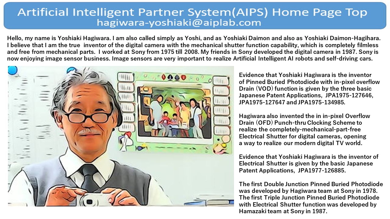
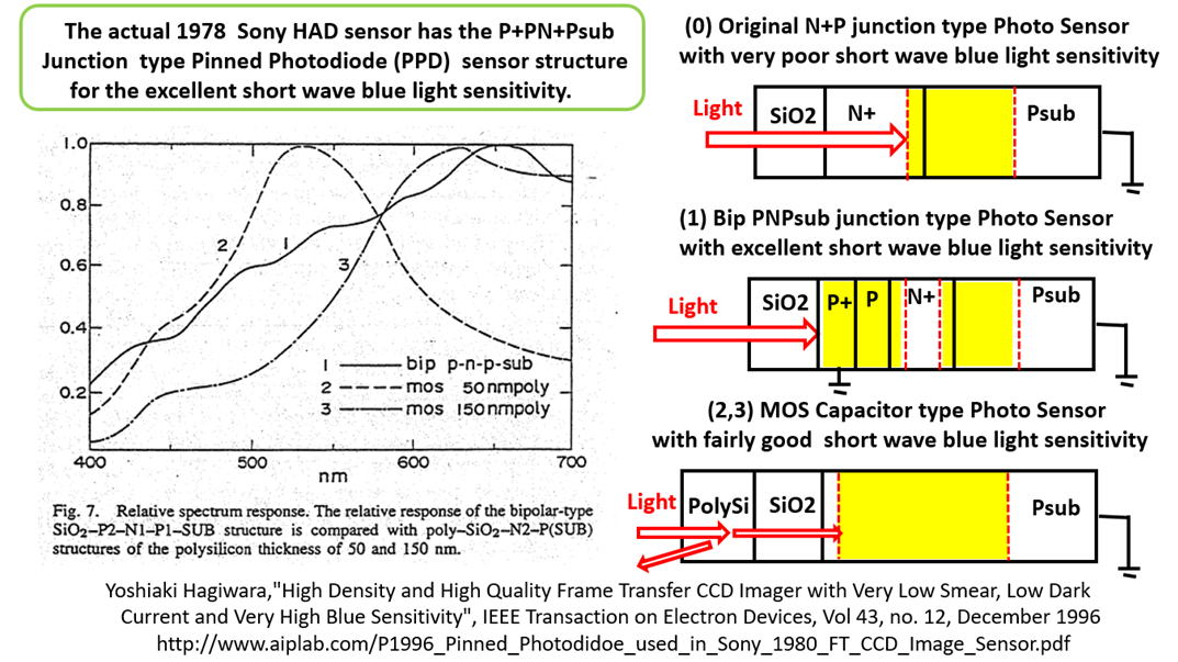
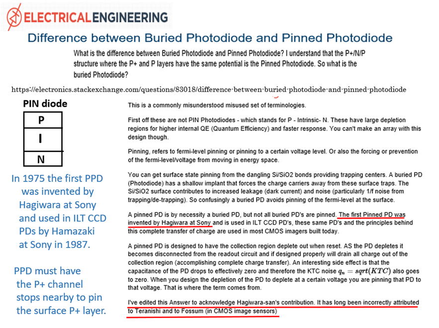
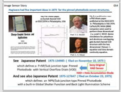
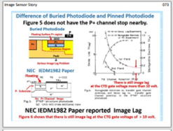
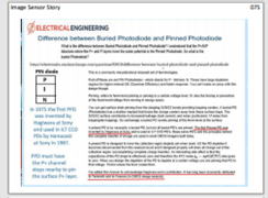
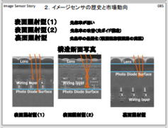
Buried Photodiode is NOT always Pinned Photodiode.
********************************************************************
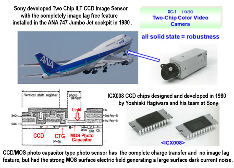
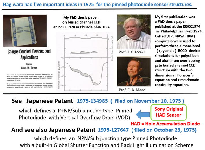
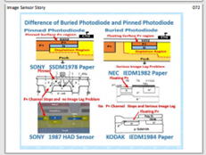
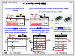
I think KODAK used PPD in the ILT CCD image sensor and reported in IEDM1984
for the first time in the world while SONY ( Hagiwara ) used PPD in the
FT CCD
image sensor and reported in SSDM1978 for the first time in the world.
********************************************************************
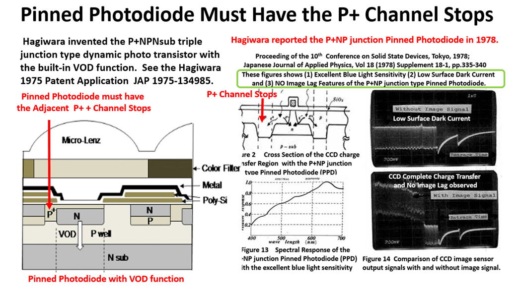
The surface thin and shallow P+ hole accumulation layer is formed
by the self-aligned ion implantation in the final processing stage.
The depth of the surface P+ hole accumulation layer
must be very shallow and less than 0. 2 micro meter
since the short wave blue light cannot penetrate
into the silicon cystal more than 0. 2 micro meter
in depth. The P+ thin layer stripe of the length L
has a large resitance R and a large capacitance C,
and then, also a large time delay constant of T=RC ,
which makes the P+ thin hole accumulaion layer
effectively floating. Therefore, this photodiode may
have a serious image lag ?? Any photodiode with
the serious image lag cannot be Pinned Photodiode.
This photodiode may not be Pinned Photodiode ????
+++++++++++++++++++++++++++++++++++++++++++++++++++++++++++++++++++
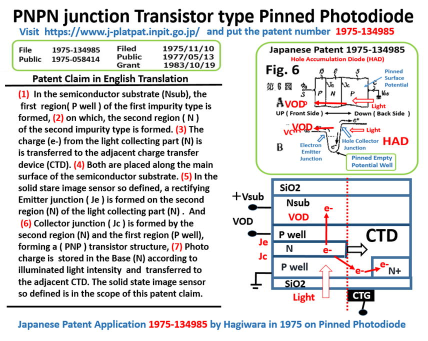
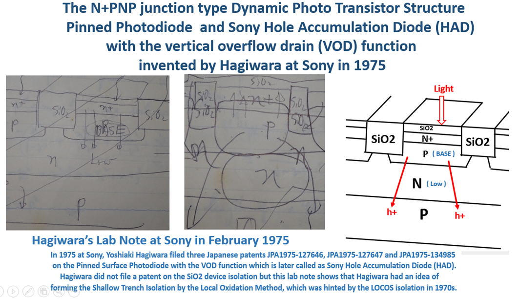
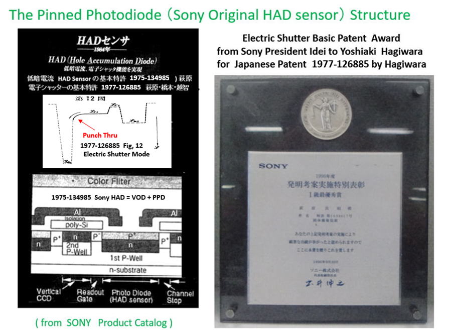
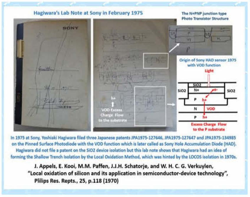
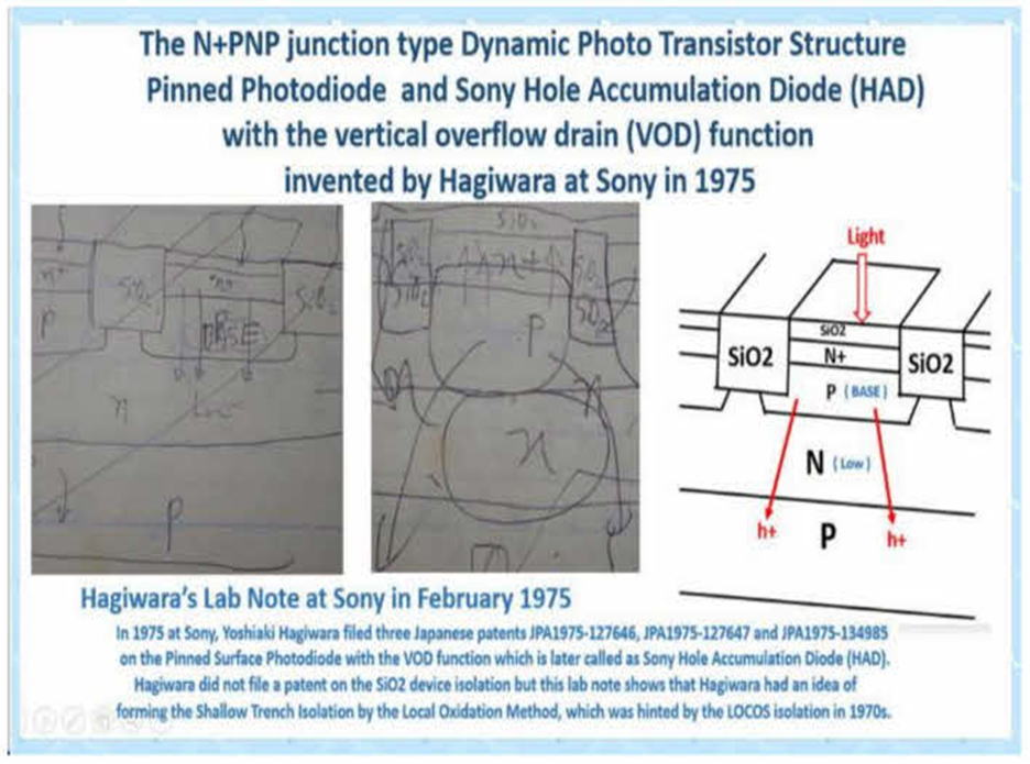
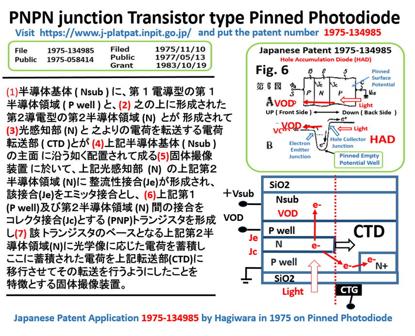
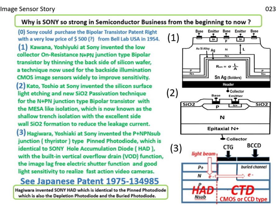
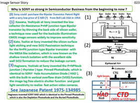
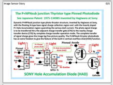
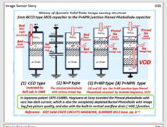
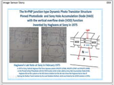
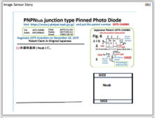
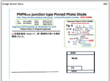
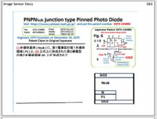
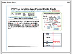
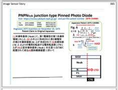
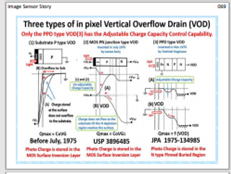
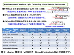
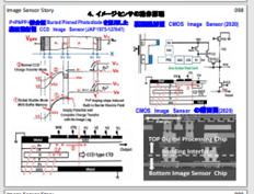
The P+NPN Triple Junction type Dynamic Thyristor Photo Sensor, which
was developped in 1987 by Hamazaki team later called as Hole Accumulation
diode(HAD) by Sony has the vertical overflow drain (VOD) and the eletrical
shutter funtion. This P+NPN Triple Junction type Dynamic Thyristor Photo
Sensor was also invented by Yoshiaki Hagiwara at Sony in 1975. See also
the Patent Applications, JPA 1975-127646, 1975-127647 and 1975-134985.
+++++++++++++++++++++++++++++++++++++++++++++++++++++++++++++++++++
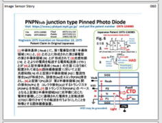
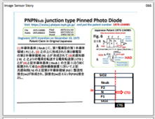
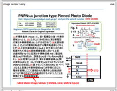
Hagiwara at Sony is the inventor and also the developper of the P+NP double
junction type Pinned Photodiode. Hagiwara also invented the P+NPN triple
junction type Pinned Photodiode with the vertical overflow drain (VOD) and
the electrical shutter function.
In 1987, the Hamazaki team in Sony developed the P+NPN triple junction type
Pinned Photodiode, named it as Hole Acculation Diode (HAD) and used it in
Interline Transfer Type CCD Image Sensors.
![]()
+++++++++++++++++++++++++++++++++++++++++++++++++++++++++++++++++++
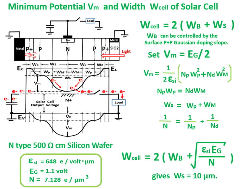
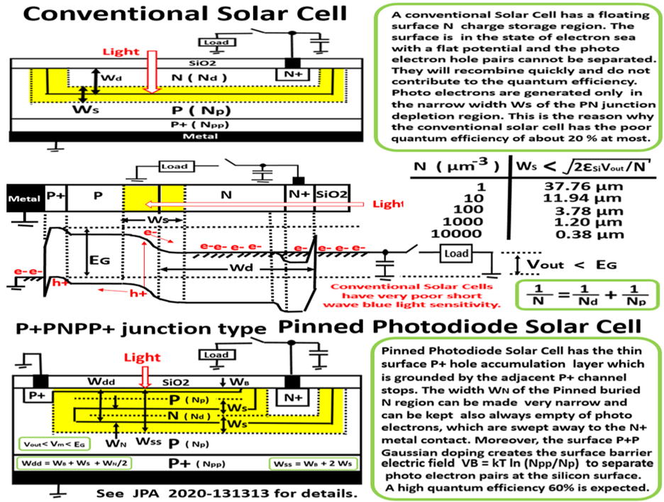
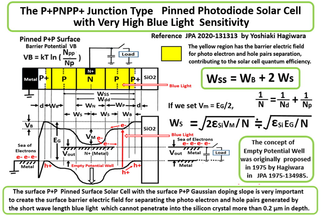
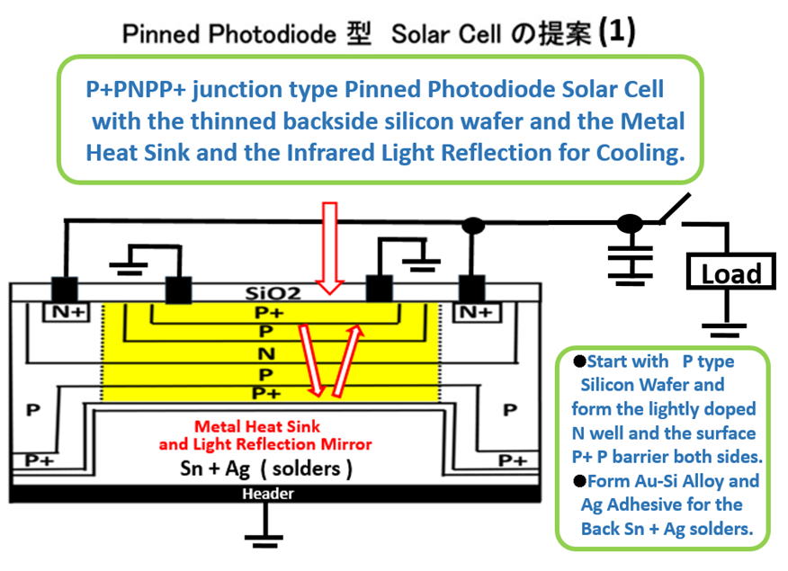
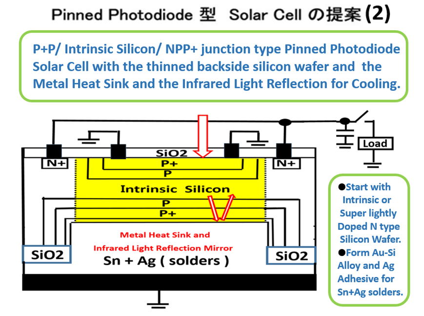
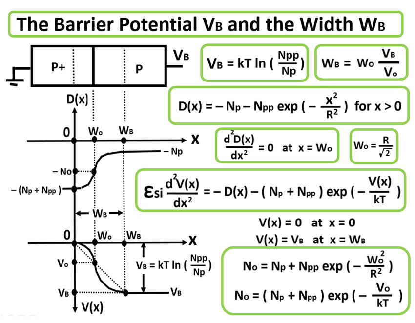
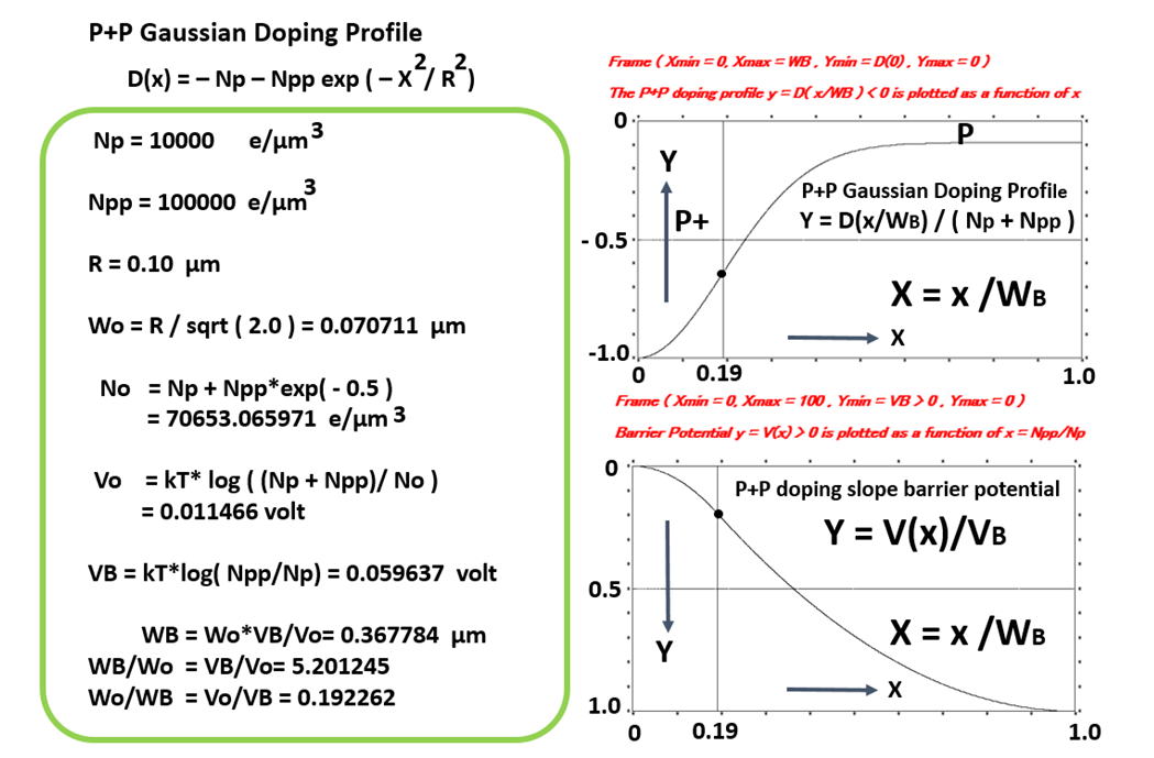
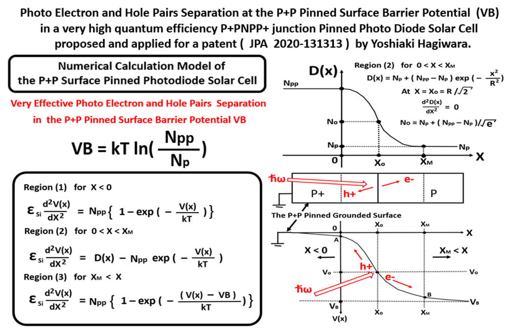
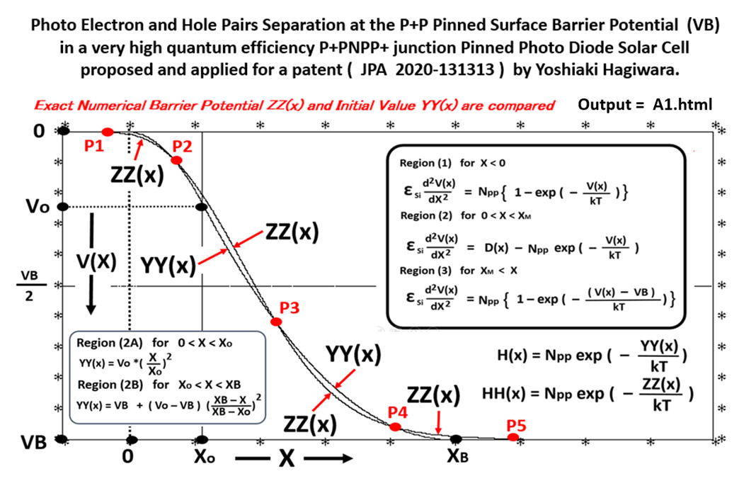
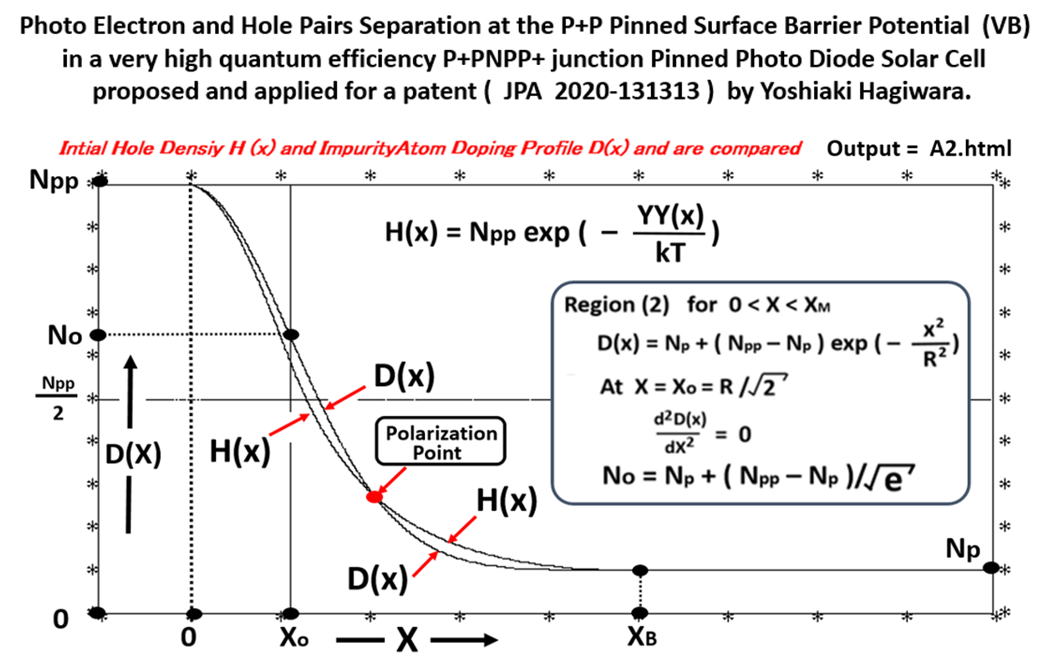
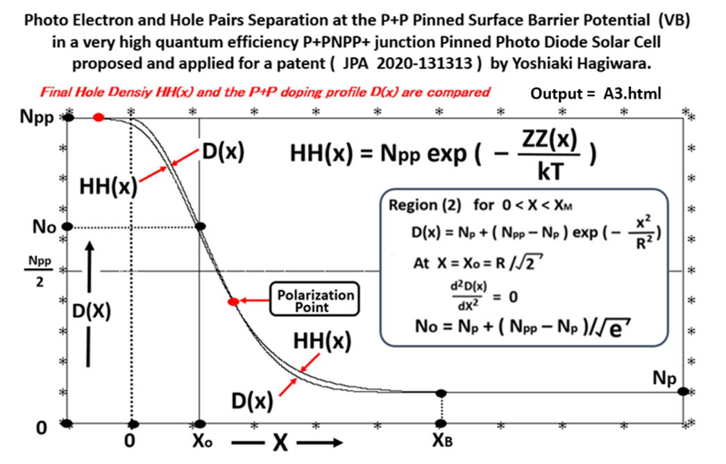
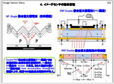
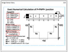
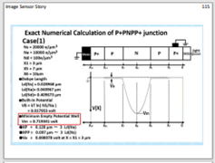
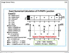
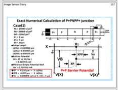
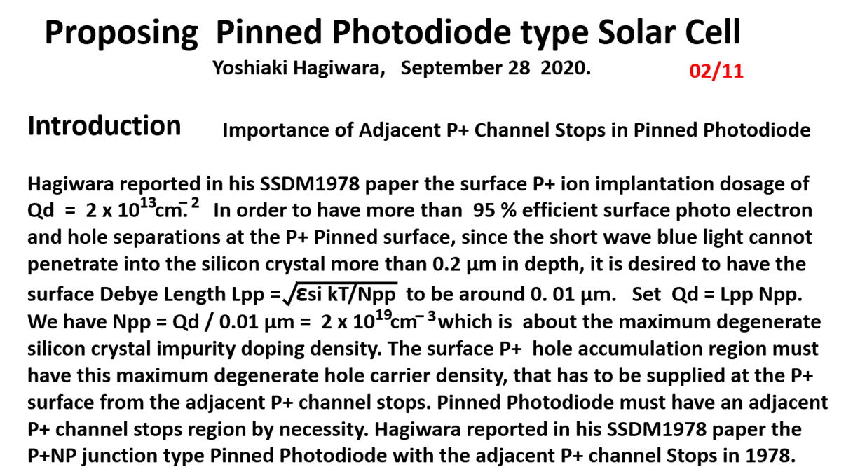
The P+PNPP+ double junction type Pinned Photodiode type Solar Cell
+++++++++++++++++++++++++++++++++++++++++++++++++++++++++++++++++++
Most of the solar cells are still of the N+P single junction type.
Here now the Pinned surface P+PNPP+ double junction type Solar Cell
is proposed, which is expected to have a very large quantum efficiency
of more than junction 60% , by using the surface hole accumulation (HAD)
region with the pinned P+P surface and the surface barrier potential
which separates the hole electron pairs generated by the short wave blue
light very effectively in the pinned silicon P+P surface barrier electric field.
A very hige efficient Pinned Photodiode (HAD) type Solar Cell is expected
to be manufactured with a very cost-effective simple fabrication process.
+++++++++++++++++++++++++++++++++++++++++++++++++++++++++++++++++++++
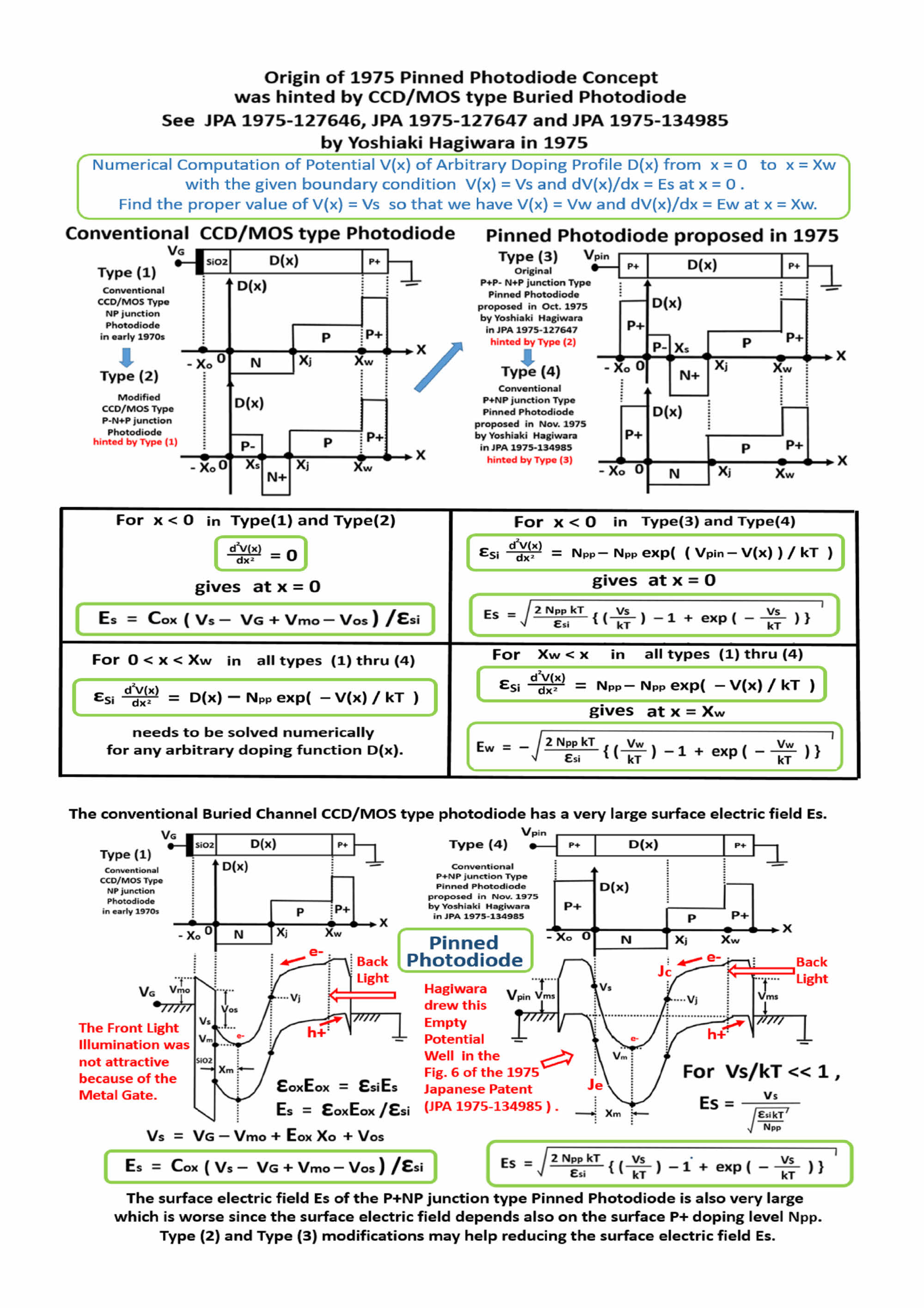
************************************************
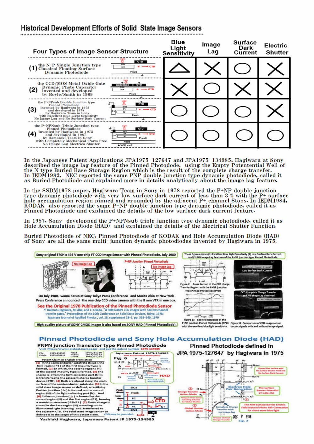
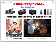
What is Pinned Photodiode ?
*************************************************
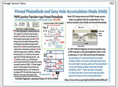
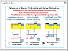
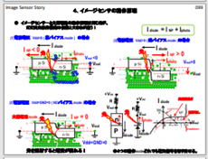
Pinned Photodiode is a double junction type photodiode
with the buried charge collection storage (base) region
and with the pinned surface flat potential fixed by the
adjacent channel stops. This unique photodiode has
many wonderful features that realized the modern solid
state electric eye for AI Robot Vision.
The pinned surface potential gives the flat surface
potential with no surface electric field. Hence there
is no surface electric induced surface dark current.
The signal charge stored in the buried storage (base)
region can be transfered compleletly to the adjacent
charge transfer gate (CTD) with no image lag feature.
The complete photo signal charge transfer results in
the completely empty potential well in the buried
storage (base) region which is the evidence of the
image lag free picture quality for action movie cameras.
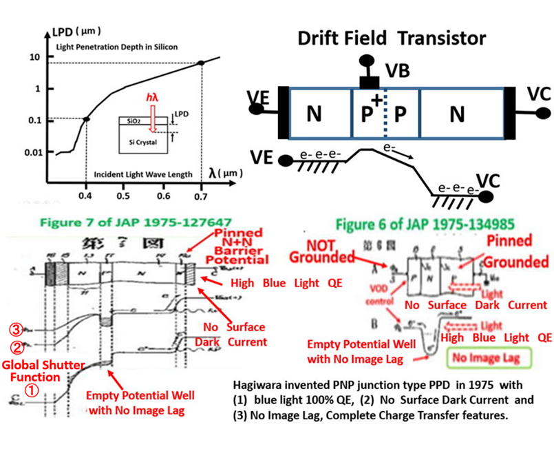
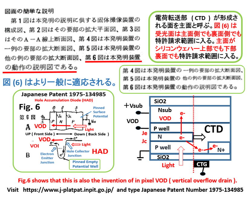
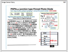
Yoshiaki Hagiwara at Sony in 197,for the first time in
the world, drew this empty potential wells in the Fig. 6
of his Japanese patent application JPA 1975-134985 and
also Fig. 7 of JPA 1975-127646 and JPA 1975-127647.
************************************************
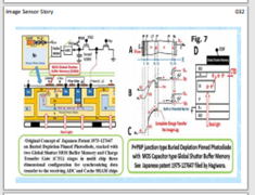
*******************************************************************
Fig.7 of JPA 1975-127647, the original Japanese patent on the double
junction type Pinned Photodiode shows the empty potential well which
implies the complete charge transfer operation of no image lag feature.
This is the evidence that Hagiwara is the true inventor of Pinned Photodiode.
******************************************************************
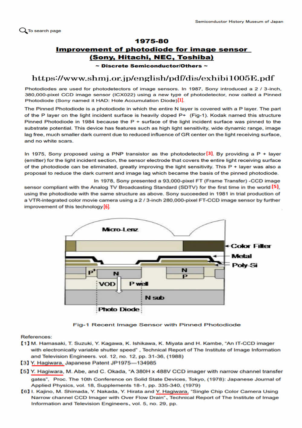
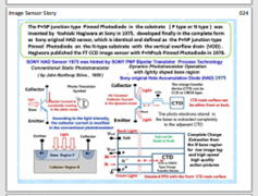
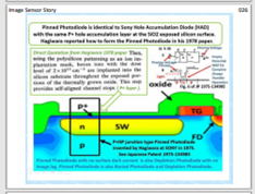
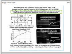
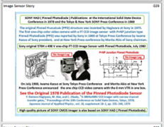
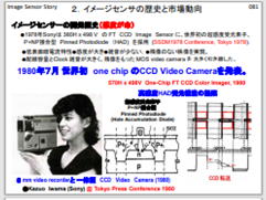
Sony developed the double junction type Pinned Photodiode in 1978 and
reported
in SSDM1978 paper. And Then Sony used this double junction type Pinned
Photodiode for the one chip video movie camera in 1980.
Sony developed the triple junction type Pinned Photodiode in 1987 with
the
complete Electric Shutter Function with no image lag and for action pictures.
This triple junction type Pinned Photodiode shown above and defined in
the
Japanese Patent Application JPA 1975-134985 was originally hinted by the
triple junction type Pinned Photodiode defined in Japanese Patent Application
JPA 1975-127646 shown below which is also inventedby Hagiwara in 1975.
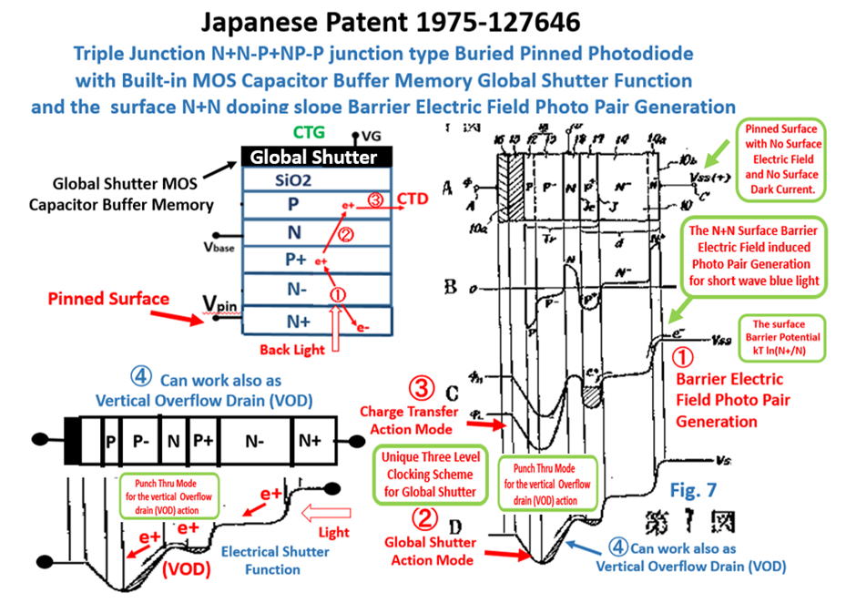
Hagiwara is the inventor of the Electrical Shutter Function of Pinned Photodiode.
Electric Shutter Function is possible only in the image lag free photo
sensors.
Only the CCD/MOS capacior type photo sensors
and Pinned Photodiode type photo sensors are
the complete image lag free photo sensors.
Only the classical CCD/MOS capacitor type
and the triple junction type Pinned Photodiode,
invented by Hagiwara in 1975, can serve for
the completely filmless cameras, which is also
completely free from any mechanical parts.
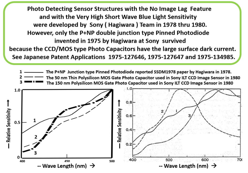
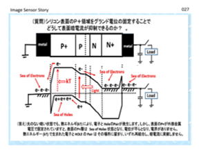
CCD/MOS photo capacitor has the serioous large surface dark current problem.
Hagiwara invented the double and triple junction Pinned Photodiodes with
the
Pinned Surface P+ Emitter region and the Buried Base Photo Charge Storage
region with the complete charge transfer function capability with no image
lag.
http://www.aiplab.com/NPNP_junction_Pinned_Photodiode_in_1975_by_Hagiwara_A.jpg
http://www.aiplab.com/JP1975-127647_A.jpg
http://www.aiplab.com/JP1975-134985_Patent_Claim_in_English.jpg
http://www.aiplab.com/JP1975-127646_A.jpg
http://www.aiplab.com/P1978_SSDM1978_Paper_on_Pinned_Photodiode_A.jpg
http://www.aiplab.com/Pinned_Photodiode_Reported_in_Hagiwara_SSDM1978_Paper.jpg
http://www.aiplab.com/What_is_True_Pinned_Photodiode.jpg
![]()
*****************************************************************
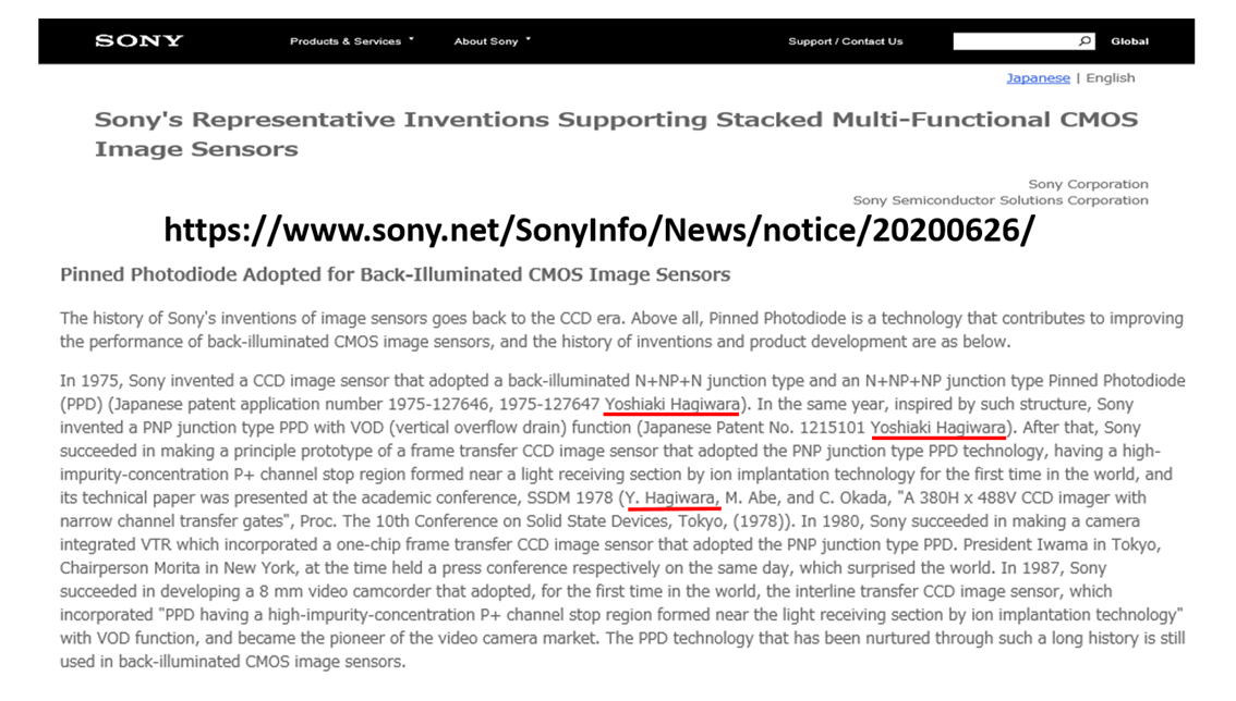
The Evidence that Hagiwara at Sony is the inventer of Pinned Photodiode
is
given by the three 1975 Japanese Patent Applications , JPA 1975-127646,
JPA 1975-127647 and JPA 1975-134985. Details are explained below.
*****************************************************************
Hagiwara is also the inventor of the Global Shutter Function
needed in the modern CMOS Image Sensors. For the details,
please read the conference publication papers:
http://www.aiplab.com/P2019_3DIC2019Paper_on_3D_Pinned_Photodiode.pdf
http://www.aiplab.com/P2020_EDTM2020_PaperID_3C4_by_Hagiwara.pdf
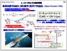
Pinned Photodiode has an excellent short wave blue light sensitivity
that can be also applied to the Pinned Photodiode type Solar Cells.
http://www.aiplab.com/P2020_Pinned_Photodiode_Solar_Cell_1.pdf
http://www.aiplab.com/P2020_Pinned_Photodiode_Solar_Cell_2.pdf
************************************************************
Hagiwara at Sony invented Pinned Photodiode in 1975
index000_Invention_of_Pinned_Photodiode_in_1975.html
index001_Image_Sensor_1975_1977_and_2014_Patents.html
index002_Facts_on_Invention_of_Pinned_Photodiode.html
index003_Hagiwara_Publication_List.html
index004_My_Wonderful_Memory_Pictures.html
index005_Image_Sensor_Story_by_Hagiwara.html
index006_Slide_Sony_Atsugi_Tech_2020_07_10.html
*************************************************************
http://www.aiplab.com/Memo_2020_09_17_by_Yoshiaki_Hagiwara.html
![]()
http://www.aiplab.com/JP1975-134985.pdf

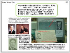

Who invented the Pinned Photodiode ?
Yoshiaki Hagiwara invented Pinned Photodiode in 1975.
Who invented the Electric Shutter ?
Yoshiaki Hagiwara invented Electric Shutter in 1975.
![]()
Who invented the Global Shutter ?
Yoshiaki Hagiwara invented Electric Shutter in 1975.
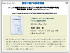
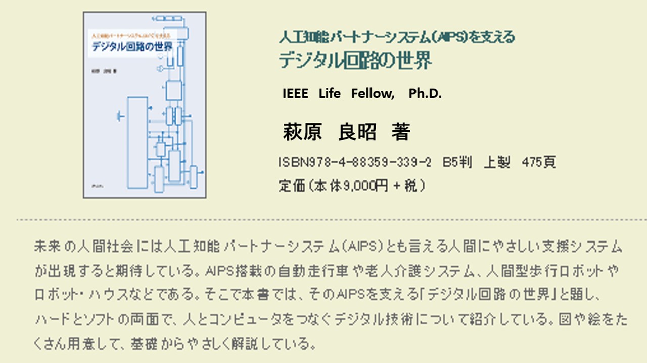
Yoshiaki Hagiwara wrote a book on
"the World of Artificial Intelligent Digital Circuits",
which is important and needed to built
the intelligent image sensor systems.
ISBM978-4-88359-339-2
Hard Cover, 460 page,
\ 9000 Japanese Yen + tax
If you are interestied in the book, Please visit
https://www.seizansha.co.jp/ISBN/ISBN978-4-88359-339-2.html
https://www.seizasha.co.jp/
Hagiwara at Sony invented Pinned Photodiode in 1975.
http://www.aiplab.com/Hagiwara_invented_PPD_and_Sony_HAD_in_1975.pdf
**************************************************************
単純質問豆知識:
(1) CCD カメラと CMOSカメラの違いは何ですか?
(2) CMOS Image Sensor は CMOS Processで造れますか?
**************************************************************
(1) CCD カメラと CMOSカメラの違いは何ですか?
**************************************************************
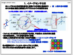
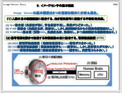
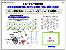
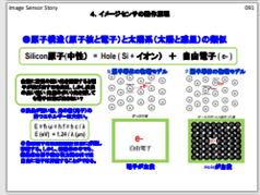
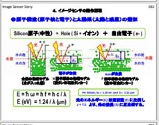
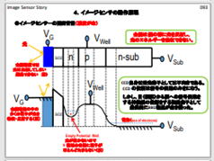
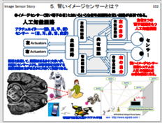
●イメージセンサーには2つの部分に別れますが、
光電変換素子(A)と電荷転送装置(B)です。
光信号エネルギーを電気信号エネルギーに
変換する光電変換素子(A)がまずあります。
光電変換原理はイメージセンサーも
太陽電池も同じ動作原理です。
光電変換装置(A)は N+P接合容量(A1)から、
CCD/MOS容量(A2)、P+NP double 接合容量(A3),
そしてさらにP+NPN triple 接合容量(A3)に進化しました。
電荷転送装置(B)は MOS型(B1)電荷転送装置、
CCD型(B2) 電荷転送装置、そして今では、
CMOS型(B3)電荷転送装置に進化しました。
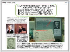
CCD カメラと CMOSカメラの違いは単純に電荷転送装置の部分の違いです。
アナログTV時代は、CCD型(B2) 電荷転送装置の性能で充分でしたが
デジタルTV時代では、CCD型(B2) 電荷転送装置の性能では不十分に
なりました。CCDはもう必要なくなりました。その代わりに、CMOSの
微細加工技術の進化に伴い、CMOS型(B3)電荷転送装置が実用
耐えるほど進化しました。それで現在は CMOS カメラが市場制覇しています。
**************************************************************
(2) CMOS Image Sensor は CMOS Processで造れますか?
**************************************************************
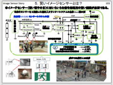
●CMOS Image Sensor の製作プロセスフローは
一般のCMOS Image Sensor Process より複雑ですが
CCD Image Sensor の Process ほど 難しくは
ありません。生産 Knowhow も必要ありません。
しかし裏面照射型のCCD Image Sensorの製法になると、
たいへん異なります、というか、非常に複雑で長い
プロセスフローになります。。
●シリコンウェーハ―の表面から裏面まで深い井戸を
シリコン結晶に小さなん穴を無数に掘り、その中に
金属(Cu)を埋める工程なども含みます。
●イメージセンサーには2つの部分に別れますが、
光電変換素子(A)と電荷転送装置(B)です。
光信号エネルギーを電気信号エネルギーに
変換する光電変換素子(A)がまずあります。
光電変換原理はイメージセンサーも
太陽電池も同じ動作原理です。
光電変換装置(A)は N+P接合容量(A1)から、
CCD/MOS容量(A2)、P+NP double 接合容量(A3),
そしてさらにP+NPN triple 接合容量(A3)に進化しました。
電荷転送装置(B)は MOS型(B1)電荷転送装置、
CCD型(B2) 電荷転送装置、そして今では、
CMOS型(B3)電荷転送装置に進化しました。
●その電気信号エネルギー(電荷)はアナログ信号
ですのでまず高速に AD変換し、デジタル信号にして出力
します。イメージセンサーの入力生制御信号も、AD変換
された信号ですので、デジタル映像信号です。それが今では
そのままデジタルTVに入力されます。
●デジタル映像信号(1と0)を処理する
のは CMOS LOGIC 回路で充分です。
●それで、イメージセンサーのChip内面積の周辺部分は
ほとんどCMOS LOGIC回路であり、CMOS LOGIC
Processで充分ですが、中央の光電変換部分が特に
CMOS LOGIC Process と異なります。
●しかし、イメージセンサー光電変換素子や信号電荷を
転送する回路装置が必要となり、機能が多くなるほど、
それに応じてプロセス工程も複雑になりますが、
そのぶん、複雑でたいへん有用な機能が実現します。
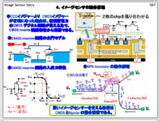
●8-24に断面図は裏面照射型の最新の
CMOS イメージセンサーの断面図です。
●周辺にはCMOS LOGIC回路を使っていますが、
中央の光電変換回路は NMOS のSwitch 回路だけで
PMOS 回路は使っていません。イメージセンサーの中央部分は
NMOS回路と Bipolar 回路が融合したものです。
●中央には 光電変換素子を形成するために
PNP 接合がいろいろあり、NMOSプロセスと Bipolar
トランジスタをごちゃまぜにした非常に複雑なプロセスです。
●それでも、出力映像信号は、普通のCMOS LOGIC
回路から出力されたデジタル映像信号ですので、今は
CMOS Image Sensor と呼ばれています。
**************************************************************
Hagiwara at Sony invented Pinned Photodiode in 1975
index000_Invention_of_Pinned_Photodiode_in_1975.html
index001_Image_Sensor_1975_1977_and_2014_Patents.html
index002_Facts_on_Invention_of_Pinned_Photodiode.html
index003_Hagiwara_Publication_List.html
index004_My_Wonderful_Memory_Pictures.html
index005_Image_Sensor_Story_by_Hagiwara.html
index006_Slide_Sony_Atsugi_Tech_2020_07_10.html
*************************************************************
http://www.aiplab.com/Proposal_of_Pinned_Photodiode_type_Solar_Cell_2020_09_28.html
http://www.aiplab.com/Memo_2020_09_20_by_Yoshiaki_Hagiwara.html
http://www.aiplab.com/Memo_2020_09_17_by_Yoshiaki_Hagiwara.html
http://www.aiplab.com/Memo_2020_08_29_by_Yoshiaki_Hagiwara.html
http://www.aiplab.com/Memo_2020_08_23_by_Yoshiaki_Hagiwara.html
http://www.aiplab.com/Memo_2020_08_21_by_Yoshiaki_Hagiwara.html
***************************************************************
***********************************************************
Hagiwara Publication List
*********************************************************
Please visit for details
http://www.aiplab.com/index003_Hagiwara_Publication_List.html
*******************************************
Basic Patent Applications on Pinned Photodiode
*******************************************
http://www.aiplab.com/JP1975-127646.pdf
http://www.aiplab.com/JP1975-127647.pdf
http://www.aiplab.com/JP1975-134985.pdf
http://www.aiplab.com/JP1977-126885.pdf
*******************************************
Pinned Photodiode Papers published by Hagiwara
*******************************************
http://www.aiplab.com/P1978_Pinned_Photodiode_1978_Paper_by_Hagiwara.pdf
https://www.imagesensors.org/Past%20Workshops/1979%20CCD79/03-1%20Hagiwara.pdf
http://www.aiplab.com/P1996_Pinned_Photodidoe_used_in_Sony_1980_FT_CCD_Image_Sensor.pdf
http://www.aiplab.com/P2001_ESSCIRC2001.pdf
http://www.aiplab.com/P2008_ESSCIRC2008Hagiwara.pdf
http://www.aiplab.com/P2019_3DIC2019Paper_on_3D_Pinned_Photodiode.pdf
http://www.aiplab.com/P2020_EDTM2020_PaperID_3C4_by_Hagiwara.pdf
****************************************************
****************************************************
Unpublished Works on the Pinned Photodiode type Solar Cell
****************************************************
http://www.aiplab.com/P2020_Pinned_Photodiode_Solar_Cell_1.pdf
http://www.aiplab.com/P2020_Pinned_Photodiode_Solar_Cell_2.pdf
****************************************************
************************************************************
Slides related to the Pinned Photodiode invented by Hagiwara in 1975
************************************************************
http://www.aiplab.com/JP1975-127647_A.jpg
http://www.aiplab.com/JP1975-134985_Patent_Claim_in_English.jpg
http://www.aiplab.com/JP1975-127646_A.jpg
http://www.aiplab.com/P1978_SSDM1978_Paper_on_Pinned_Photodiode_A.jpg
http://www.aiplab.com/Pinned_Photodiode_Reported_in_Hagiwara_SSDM1978_Paper.jpg
http://www.aiplab.com/What_is_True_Pinned_Photodiode.jpg
http://www.aiplab.com/NPNP_junction_Pinned_Photodiode_in_1975_by_Hagiwara_A.jpg
http://www.aiplab.com/Origin_of_1975_Concept_of_Pinned_Photodiode_.jpg
http://www.aiplab.com/Pinne_Photodiode_Solar_Cell.jpg
http://www.aiplab.com/Solar_Cell_with_High_Blue_Light_Sensitivity.jpg
http://www.aiplab.com/Image_Sensor_Story_36.jpg
http://www.aiplab.com/Image_Sensor_Story_35.jpg
http://www.aiplab.com/Difference_of_Static_and_Dynamic_Photo_Transistor.jpg
http://www.aiplab.com/Pinned_Photodiode_Drift_Field_Trasistor.jpg
http://www.aiplab.com/P1978_SSDM1978_Paper_Lightly_Doped_Drain_Output_Cirucuit.jpg
http://www.aiplab.com/Slide023A_Sony_Atsugi_Tech_2020_07_10.jpg
**************************************************************************
AIPS Library Under Construction Now
*********************************************************************
Please write me freely anything related to my activities:
*********************************************************************
hagiwara-yoshiaki@aiplab.com for my activity at http://www.aiplab.com/
hagiwara@ssis.or.jp for my activity at http://www.ssis.or.jp/en/index.html
*********************************************************************
******************************
Return to Top Page
http://www.aiplab.com/
*********************************
**************************************************************
This is index_2020_12_07_005.html
**************************************************************
Jump to Part 001 002 003 004 005 006 007 008 009 010 011 012 013
**************************************************************