**************************************************************
This is index_2020_12_07_013.html
**************************************************************
Jump to Part 001 002 003 004 005 006 007 008 009 010 011 012 013
**************************************************************
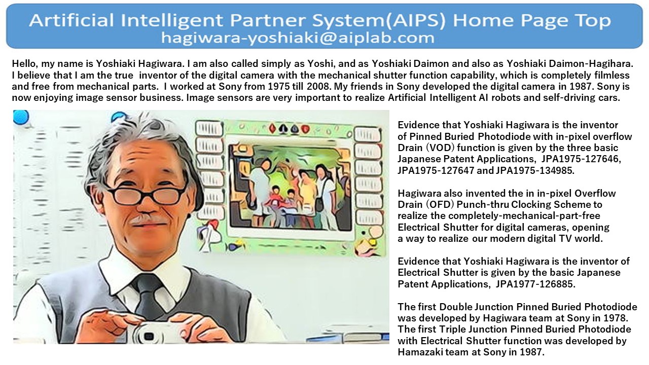
Hagiwara at Sony invented Pinned Photodiode in 1975
index000_Invention_of_Pinned_Photodiode_in_1975.html
index001_Image_Sensor_1975_1977_and_2014_Patents.html
index002_Facts_on_Invention_of_Pinned_Photodiode.html
index003_Hagiwara_Publication_List.html
index004_My_Wonderful_Memory_Pictures.html
index005_Image_Sensor_Story_by_Hagiwara.html
index006_Slide_Sony_Atsugi_Tech_2020_07_10.html
*************************************************************
http://www.aiplab.com/Proposal_of_Pinned_Photodiode_type_Solar_Cell_2020_09_28.html
http://www.aiplab.com/Memo_2020_09_20_by_Yoshiaki_Hagiwara.html
http://www.aiplab.com/Memo_2020_09_17_by_Yoshiaki_Hagiwara.html
http://www.aiplab.com/Memo_2020_08_29_by_Yoshiaki_Hagiwara.html
http://www.aiplab.com/Memo_2020_08_23_by_Yoshiaki_Hagiwara.html
http://www.aiplab.com/Memo_2020_08_21_by_Yoshiaki_Hagiwara.html
***************************************************************
***********************************************************
Hagiwara Publication List
*********************************************************
Please visit for details
http://www.aiplab.com/index003_Hagiwara_Publication_List.html
*******************************************
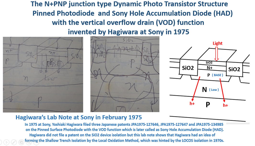
Basic Patent Applications on Pinned Photodiode
*******************************************
http://www.aiplab.com/JP1975-127646.pdf
http://www.aiplab.com/JP1975-127647.pdf
http://www.aiplab.com/JP1975-134985.pdf
http://www.aiplab.com/JP1977-126885.pdf
*******************************************
Pinned Photodiode Papers published by Hagiwara
*******************************************
http://www.aiplab.com/P1978_Pinned_Photodiode_1978_Paper_by_Hagiwara.pdf
https://www.imagesensors.org/Past%20Workshops/1979%20CCD79/03-1%20Hagiwara.pdf
http://www.aiplab.com/P1996_Pinned_Photodidoe_used_in_Sony_1980_FT_CCD_Image_Sensor.pdf
http://www.aiplab.com/P2001_ESSCIRC2001.pdf
http://www.aiplab.com/P2008_ESSCIRC2008Hagiwara.pdf
http://www.aiplab.com/P2019_3DIC2019Paper_on_3D_Pinned_Photodiode.pdf
http://www.aiplab.com/P2020_EDTM2020_PaperID_3C4_by_Hagiwara.pdf
****************************************************
****************************************************
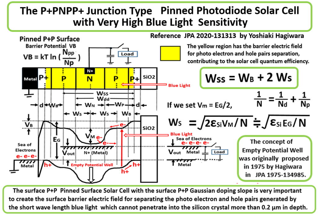
Unpublished Works on the Pinned Photodiode type Solar Cell
****************************************************
http://www.aiplab.com/P2020_Pinned_Photodiode_Solar_Cell_1.pdf
http://www.aiplab.com/P2020_Pinned_Photodiode_Solar_Cell_2.pdf
****************************************************
************************************************************
Slides related to the Pinned Photodiode invented by Hagiwara in 1975
************************************************************
http://www.aiplab.com/JP1975-127647_A.jpg
http://www.aiplab.com/JP1975-134985_Patent_Claim_in_English.jpg
http://www.aiplab.com/JP1975-127646_A.jpg
http://www.aiplab.com/P1978_SSDM1978_Paper_on_Pinned_Photodiode_A.jpg
http://www.aiplab.com/Pinned_Photodiode_Reported_in_Hagiwara_SSDM1978_Paper.jpg
http://www.aiplab.com/What_is_True_Pinned_Photodiode.jpg
http://www.aiplab.com/NPNP_junction_Pinned_Photodiode_in_1975_by_Hagiwara_A.jpg
http://www.aiplab.com/Origin_of_1975_Concept_of_Pinned_Photodiode_.jpg
http://www.aiplab.com/Pinne_Photodiode_Solar_Cell.jpg
http://www.aiplab.com/Solar_Cell_with_High_Blue_Light_Sensitivity.jpg
http://www.aiplab.com/Image_Sensor_Story_36.jpg
http://www.aiplab.com/Image_Sensor_Story_35.jpg
http://www.aiplab.com/Difference_of_Static_and_Dynamic_Photo_Transistor.jpg
http://www.aiplab.com/Pinned_Photodiode_Drift_Field_Trasistor.jpg
http://www.aiplab.com/P1978_SSDM1978_Paper_Lightly_Doped_Drain_Output_Cirucuit.jpg
http://www.aiplab.com/Slide023A_Sony_Atsugi_Tech_2020_07_10.jpg
**************************************************************************
AIPS Library Under Construction Now
*********************************************************************
Please write me freely anything related to my activities:
*********************************************************************
hagiwara-yoshiaki@aiplab.com for my activity at http://www.aiplab.com/
hagiwara@ssis.or.jp for my activity at http://www.ssis.or.jp/en/index.html
*********************************************************************
******************************
Return to Top Page
http://www.aiplab.com/
********************************* **************************************************************
This is index_2020_12_07_013.html
**************************************************************
Jump to Part 001 002 003 004 005 006 007 008 009 010 011 012 013
**************************************************************